EP2451069A1 - Branche de commutation pour redresseur à trois niveaux et procédé pour contrôler la branche de commutation pour redresseur à trois niveaux - Google Patents
Branche de commutation pour redresseur à trois niveaux et procédé pour contrôler la branche de commutation pour redresseur à trois niveaux Download PDFInfo
- Publication number
- EP2451069A1 EP2451069A1 EP10187837A EP10187837A EP2451069A1 EP 2451069 A1 EP2451069 A1 EP 2451069A1 EP 10187837 A EP10187837 A EP 10187837A EP 10187837 A EP10187837 A EP 10187837A EP 2451069 A1 EP2451069 A1 EP 2451069A1
- Authority
- EP
- European Patent Office
- Prior art keywords
- diode
- switching branch
- switch
- reverse blocking
- controlling
- Prior art date
- Legal status (The legal status is an assumption and is not a legal conclusion. Google has not performed a legal analysis and makes no representation as to the accuracy of the status listed.)
- Granted
Links
- 238000000034 method Methods 0.000 title claims abstract description 19
- 230000000903 blocking effect Effects 0.000 claims abstract description 29
- 230000007935 neutral effect Effects 0.000 claims abstract description 16
- 238000004590 computer program Methods 0.000 claims description 9
- 239000004065 semiconductor Substances 0.000 claims description 4
- 230000015654 memory Effects 0.000 description 4
- 238000010586 diagram Methods 0.000 description 3
- 238000012545 processing Methods 0.000 description 3
- 238000009826 distribution Methods 0.000 description 2
- 230000005669 field effect Effects 0.000 description 2
- 239000003990 capacitor Substances 0.000 description 1
- 230000001419 dependent effect Effects 0.000 description 1
- 238000013461 design Methods 0.000 description 1
- 230000000694 effects Effects 0.000 description 1
- 230000006870 function Effects 0.000 description 1
- 238000004519 manufacturing process Methods 0.000 description 1
- 238000005259 measurement Methods 0.000 description 1
- 238000012986 modification Methods 0.000 description 1
- 230000004048 modification Effects 0.000 description 1
- 230000003287 optical effect Effects 0.000 description 1
- 238000003860 storage Methods 0.000 description 1
- 230000003936 working memory Effects 0.000 description 1
Images
Classifications
-
- H—ELECTRICITY
- H02—GENERATION; CONVERSION OR DISTRIBUTION OF ELECTRIC POWER
- H02M—APPARATUS FOR CONVERSION BETWEEN AC AND AC, BETWEEN AC AND DC, OR BETWEEN DC AND DC, AND FOR USE WITH MAINS OR SIMILAR POWER SUPPLY SYSTEMS; CONVERSION OF DC OR AC INPUT POWER INTO SURGE OUTPUT POWER; CONTROL OR REGULATION THEREOF
- H02M7/00—Conversion of ac power input into dc power output; Conversion of dc power input into ac power output
- H02M7/02—Conversion of ac power input into dc power output without possibility of reversal
- H02M7/04—Conversion of ac power input into dc power output without possibility of reversal by static converters
- H02M7/12—Conversion of ac power input into dc power output without possibility of reversal by static converters using discharge tubes with control electrode or semiconductor devices with control electrode
- H02M7/21—Conversion of ac power input into dc power output without possibility of reversal by static converters using discharge tubes with control electrode or semiconductor devices with control electrode using devices of a triode or transistor type requiring continuous application of a control signal
- H02M7/217—Conversion of ac power input into dc power output without possibility of reversal by static converters using discharge tubes with control electrode or semiconductor devices with control electrode using devices of a triode or transistor type requiring continuous application of a control signal using semiconductor devices only
-
- H—ELECTRICITY
- H02—GENERATION; CONVERSION OR DISTRIBUTION OF ELECTRIC POWER
- H02M—APPARATUS FOR CONVERSION BETWEEN AC AND AC, BETWEEN AC AND DC, OR BETWEEN DC AND DC, AND FOR USE WITH MAINS OR SIMILAR POWER SUPPLY SYSTEMS; CONVERSION OF DC OR AC INPUT POWER INTO SURGE OUTPUT POWER; CONTROL OR REGULATION THEREOF
- H02M1/00—Details of apparatus for conversion
- H02M1/42—Circuits or arrangements for compensating for or adjusting power factor in converters or inverters
- H02M1/4208—Arrangements for improving power factor of AC input
- H02M1/4216—Arrangements for improving power factor of AC input operating from a three-phase input voltage
-
- Y—GENERAL TAGGING OF NEW TECHNOLOGICAL DEVELOPMENTS; GENERAL TAGGING OF CROSS-SECTIONAL TECHNOLOGIES SPANNING OVER SEVERAL SECTIONS OF THE IPC; TECHNICAL SUBJECTS COVERED BY FORMER USPC CROSS-REFERENCE ART COLLECTIONS [XRACs] AND DIGESTS
- Y02—TECHNOLOGIES OR APPLICATIONS FOR MITIGATION OR ADAPTATION AGAINST CLIMATE CHANGE
- Y02B—CLIMATE CHANGE MITIGATION TECHNOLOGIES RELATED TO BUILDINGS, e.g. HOUSING, HOUSE APPLIANCES OR RELATED END-USER APPLICATIONS
- Y02B70/00—Technologies for an efficient end-user side electric power management and consumption
- Y02B70/10—Technologies improving the efficiency by using switched-mode power supplies [SMPS], i.e. efficient power electronics conversion e.g. power factor correction or reduction of losses in power supplies or efficient standby modes
Definitions
- the invention relates to a switching branch for a three-level rectifier and a method for controlling a switching branch for a three-level rectifier.
- Three-level rectifiers are rectifiers that have three DC outputs. In addition to the positive and negative DC outputs they have a neutral DC output. Examples of three-level rectifiers are given in J. W. Kolar and F. C. Zach, "A novel three-phase utility interface minimizing line current harmonics of high-power telecommunications rectifier modules", IEEE transactions on industrial electronics, Vol. 44, No. 4, August 1997 , and in Y. Zhao, Y. Li and T. A. Lipo, "Force commutated three level boost type rectifier", IEEE transactions on industry applications, Vol. 31, No. 1, January/February 1995 .
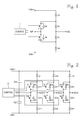
- Figure 1 shows an example of a switching branch for a three-level rectifier comprising six diodes D1 to D6 and two controllable switches S1, S2.
- the switches are controlled via a control arrangement 10 according to a modulation scheme used.
- Possible modulation methods are vector modulation and hysteresis modulation, for example.
- the first switch S1 When current flows towards the rectifier from an AC input pole of the rectifier branch, the first switch S1 is modulated and the first diode D1 and the first switch S1 commutate with each other according to the modulation scheme used.
- the second switch S2 is modulated and the fourth diode D4 and the second switch S2 commutate with each other according to the modulation scheme used.
- a rectifier configuration may also include an AC filter (not shown in the figures), which may be e.g. of L-type or LCL-type and which is connected between the rectifier input pole(s) and corresponding poles of the supplying AC voltage source.
- a problem related to the above example is an uneven distribution of voltage across components in a reverse blocking state.
- a reason for this may be impedance differences due to different component characteristics, component manufacturing or circuit configuration.
- the third and fourth diodes D3 and D4 are in the reverse blocking state and if a reverse impedance of the fourth diode D4 is higher than the reverse impedance of the third diode D3, the voltage across the fourth diode D4 tends to be higher than the voltage across the third diode D3.
- the sixth diode D6 connected in parallel with the second switch S2 guarantees that the voltage across the fourth diode D4 is at most the same as the potential of the neutral DC output NP because the sixth diode D6 then connects the connection point of the third and fourth diodes D3 and D4 directly to the neutral DC output NP.
- the reverse impedance of the third diode D3 is higher than the reverse impedance of the fourth diode D4 and the voltage across the third diode D3 tends to be higher than the voltage across the fourth diode D4, the sixth diode D6 stays in a reverse blocking state and does not limit the voltage across the third diode D3.
- the third diode D3 may be exposed to the total voltage Udc of the DC intermediate circuit.
- the second diode D2 may be exposed to the total voltage Udc of the DC intermediate circuit. This is not desirable.
- a solution to the problem described above is to connect additional resistors in parallel with the series-connected diodes D1 to D4 to balance the distribution of voltage across the diodes.
- additional resistors in parallel with the series-connected diodes D1 to D4 to balance the distribution of voltage across the diodes.
- additional components cause additional costs and also additional losses.
- An object of the invention is thus to provide a method and an apparatus for implementing the method so as to solve or at least alleviate the above problem.
- the object of the invention is achieved by a switching branch for a three-level rectifier, a rectifier, a method, and a computer program product that are characterized by what is stated in the independent claims. Preferred embodiments of the invention are described in the dependent claims.
- the invention is based on the idea of setting each controllable switch of the switching branch in a conducting state during the time when the switch is not modulating the input voltage of the switching branch. This may be accomplished by setting the first switch of the switching branch to be in a conductive state during the reverse blocking state of the first diode and the second diode, i.e. when the AC input pole of the switching branch is connected to the negative output pole, and by setting the second switch of the switching branch to be in a conductive state during the reverse blocking state of the third diode and the fourth diode, i.e. when the AC input pole of the switching branch is connected to the positive output pole.
- the conducting switch connects the neutral DC output potential to the connection point of the diodes in the reverse blocking state and thus the voltage stress of the diodes in the reverse blocking state is always at most about half the total voltage of the DC intermediate circuit.
- An advantage of the invention is that by controlling the switches into a conductive state when they are not modulating the input voltage of the rectifier, the voltages across the diodes in the reverse blocking state can be balanced without the use of any additional components such as resistors. This results in lower power losses and overall costs.
- the application of the invention is not limited to any specific system, but it can be used in connection with various electric systems. Moreover, the use of the invention is not limited to systems employing any specific fundamental frequency or any specific voltage level.
- FIG. 1 shows an example of a switching branch for a three-level rectifier according to an embodiment.
- the figure shows only components necessary for understanding the invention. It should be noted that the switching branch configuration could differ from the one shown in Figure 1 without deviating from the basic idea of the invention.
- the switching branch comprises a first diode D1 and a second diode D2 connected in series between a positive DC output pole Udc+ and an AC input pole AC of the switching branch.
- the switching branch further comprises a third diode D3 and a fourth diode D4 connected in series between the AC input pole AC of the switching branch and a negative DC output pole Udc-.
- the switching branch comprises a first controllable switch S1 connected between a neutral DC output pole NP and a connection point between the first and the second diode, and a second controllable switch S2 connected between the neutral DC output pole NP and a connection point between the third and the fourth diode.
- the switches S1, S2 can be semiconductor switches such as IGBT (Insulated Gate Bipolar Transistor) or FET (Field-Effect Transistor) or any corresponding controllable switches.
- the figure further shows a control arrangement 10 via which the switches S1, S2 can be controlled.
- the normal operation of the rectifier includes pulse width modulation (PWM) of the rectifier input voltage by the switches S1, S2 according to a certain modulation method.
- PWM pulse width modulation
- the exemplary switching branch of Figure 1 can further comprise a fifth diode D5 connected in parallel with the first switch S1 and a sixth diode D6 connected in parallel with the second switch S2. These fifth and sixth diodes are entirely optional and may be omitted in some configurations.
- the switching branch configuration can also include an AC filter (not shown in Figure 1 ), which may be e.g. of L-type or LCL-type, that is connected between the AC input pole and a corresponding pole of a supplying AC voltage source.
- each switch of the switching branch is set into a conducting state during the time when the switch is not modulating the input voltage of the switching branch. This can be carried out by controlling the first switch S1 of the switching branch to be in a conductive state during a reverse blocking state of the first diode D1 and the second diode D2, and controlling the second switch S2 of the switching branch to be in a conductive state during a reverse blocking state of the third diode D3 and the fourth diode D4.
- the reverse blocking state of both the first diode D1 and the second diode D2 occurs when the AC input pole AC of the switching branch is connected to the negative DC output pole Udc- potential, and can be determined e.g.
- the reverse blocking state of both the third diode D3 and the fourth diode D4 occurs when the AC input pole AC of the switching branch is connected to the positive DC output pole Udc+ potential, and can be determined e.g. on the basis of the direction of the current through the AC input pole AC.
- the AC input pole of the switching branch can be connected to the neutral DC output pole NP potential by controlling the appropriate active switch according to the current polarity.
- the other switch which is not carrying the branch current can remain in the conducting state without any effect on the AC input voltage or current.
- the switch which is used for balancing the voltages across the diodes in the reverse blocking state, can stay in the conductive state continuously as long as the diodes to be balanced remain in the reverse blocking state.
- the first switch S1 of the switching branch is controlled to be in the conductive state for each entire period of the reverse blocking state of the first diode D1 and the second diode D2, and the second switch S2 of the switching branch is controlled to be in the conductive state for each entire period of the reverse blocking state of the third diode D3 and the fourth diode D4.
- the first switch S1 of the switching branch is set to be in the conductive state whenever both the first diode D1 and the second diode D2 are in the reverse blocking state
- the second switch S2 of the switching branch is set to be in the conductive state whenever both the third diode D3 and the fourth diode D4 are in the reverse blocking state.
- a three-phase three-level rectifier can be implemented by connecting together three switching branches as described above.
- Figure 2 illustrates an exemplary circuit diagram of a rectifier according to an embodiment comprising three switching branches corresponding to that of Figure 1 .
- the three switching branches have been connected together by connecting the positive DC output poles Udc+ of each switching branch together, the negative DC output poles Udc- of each switching branch together, and the neutral DC output poles NP of each switching branch together.
- the figure shows only components necessary for understanding the invention. It should be noted that the rectifier circuit configuration could differ from the one shown in Figure 2 without deviating from the basic idea of the invention.
- the exemplary three-phase rectifier thus comprises three switching branches with AC input poles AC1, AC2 and AC3, respectively, for connecting the rectifier to the phases of a three phase AC supply (not shown).
- the rectifier configuration can also include an AC-filter, which may be e.g. of L-type or LCL-type, that is connected between the rectifier input poles and the corresponding poles of the supplying AC-voltage source. This filter is not shown in Figure 2 .
- Each switching branch comprises a first diode D11, D12, D13 and a second diode D21, D22, D23 connected in series between a positive DC output pole Udc+ of the rectifier and an AC input pole of the switching branch AC1, AC2, AC3.
- Each switching branch further comprises a third diode D31, D32, D33 and a fourth diode D41, D42, D43 connected in series between the AC input pole of the switching branch AC1, AC2, AC3 and a negative DC output pole Udc- of the rectifier.
- each switching branch comprises a first controllable switch S11, S12, S13 connected between a neutral DC output pole NP of the rectifier and a connection point between the first and the second diode, and a second controllable switch S21, S22, S23 connected between the neutral DC output pole NP of the rectifier and a connection point between the third and the fourth diode.
- the switches S11, S12, S13, S21, S22, S23 can be semiconductor switches such as IGBT (Insulated Gate Bipolar Transistor) or FET (Field-Effect Transistor) or any corresponding controllable switches.
- the figure further shows a control arrangement 10 via which the switches can be controlled.
- the normal operation of the rectifier includes pulse width modulation (PWM) of the rectifier input voltage by the switches S11, S12, S13, S21, S22, S23 according to a certain modulation method. This may be a vector modulation or a hysteresis modulation method, for example.
- PWM pulse width modulation
- This may be a vector modulation or a hysteresis modulation method, for example.
- the invention is not, however, limited to any specific modulation method.
- the modulation control can involve one or more additional control components (not shown) possibly included in the rectifier.
- Each switching branch of the exemplary rectifier of Figure 2 can further comprise a fifth diode D51, D52, D53 connected in parallel with the first switch S11, S12, S13 of each switching branch, and a sixth diode D61, D62, D63 connected in parallel with the second switch S21, S22, S23 of each switching branch.
- These fifth and sixth diodes are entirely optional and may be omitted in some configurations.
- the DC intermediate circuit of the exemplary rectifier of Figure 2 can comprise capacitors C1 and C2 as shown. The structure of the intermediate circuit could also be different, depending on the circuit configuration used.
- the first switch S11, S12, S13 and the second switch S21, S22, S23 of each switching branch are preferably controlled in a manner similar to that described above in connection with the switching branch of Figure 1 .
- the control of the switches S1, S11, S12, S13, S2, S21, S22, S23 can be performed by or via the control arrangement 10 which can also perform the normal modulation control of the switches. It is also possible to use additional or separate logical of physical units (not shown) for performing the control functionality of the invention.
- the functionality of the invention could, for example, be implemented using a separate logic arrangement which could be independent of the normal modulation control of the switches, for example.
- the control arrangement 10 and/or a separate logic arrangement controlling the switches S1, S11, S12, S13, S2, S21, S22, S23 according to any one of the above embodiments, or a combination thereof, can be implemented as one unit or as two or more separate units that are configured to implement the functionality of the various embodiments.
- the term 'unit' refers generally to a physical or logical entity, such as a physical device or a part thereof or a software routine.
- the control arrangement 10 according to any one of the embodiments may be implemented at least partly by means of one or more computers or corresponding digital signal processing (DSP) equipment provided with suitable software, for example.
- DSP digital signal processing
- Such a computer or digital signal processing equipment preferably comprises at least a working memory (RAM) providing storage area for arithmetical operations and a central processing unit (CPU), such as a general-purpose digital signal processor.
- the CPU may comprise a set of registers, an arithmetic logic unit, and a CPU control unit.
- the CPU control unit is controlled by a sequence of program instructions transferred to the CPU from the RAM.
- the CPU control unit may contain a number of microinstructions for basic operations. The implementation of microinstructions may vary depending on the CPU design.
- the program instructions may be coded by a programming language, which may be a high-level programming language, such as C, Java, etc., or a low-level programming language, such as a machine language, or an assembler.
- the computer may also have an operating system which may provide system services to a computer program written with the program instructions.
- the computer or other apparatus implementing the invention, or a part thereof, may further comprise suitable input means for receiving e.g. measurement and/or control data, and output means for outputting e.g. control data. It is also possible to use a specific integrated circuit or circuits, or discrete electric components and devices for implementing the functionality according to any one of the embodiments.
- the invention can be implemented in existing system elements or by using separate dedicated elements or devices in a centralized or distributed manner.
- Present rectifier switching branches or rectifiers can comprise processors and memory that can be utilized in the functions according to embodiments of the invention.
- all modifications and configurations required for implementing an embodiment of the invention e.g. in existing rectifier switching branches or rectifiers may be performed as software routines, which may be implemented as added or updated software routines.
- software can be provided as a computer program product comprising computer program code which, when run on a computer, causes the computer or a corresponding arrangement to perform the functionality according to the invention as described above.
- Such a computer program code may be stored or generally embodied on a computer readable medium, such as a suitable memory, e.g. a flash memory or an optical memory, from which it is loadable to the unit or units executing the program code.
- a computer program code implementing the invention may be loaded to the unit or units executing the computer program code via a suitable data network, for example, and it may replace or update a possibly existing program code.
Landscapes
- Engineering & Computer Science (AREA)
- Power Engineering (AREA)
- Rectifiers (AREA)
Priority Applications (3)
| Application Number | Priority Date | Filing Date | Title |
|---|---|---|---|
| EP10187837.9A EP2451069B1 (fr) | 2010-10-18 | 2010-10-18 | Branche de commutation pour redresseur à trois niveaux et procédé pour contrôler la branche de commutation pour redresseur à trois niveaux |
| DK10187837T DK2451069T3 (da) | 2010-10-18 | 2010-10-18 | Omskiftningsgren til tre niveau-ensretter og fremgangsmåde til styring af omskiftningsgren til tre niveau-ensretter |
| US13/275,844 US8644043B2 (en) | 2010-10-18 | 2011-10-18 | Switching branch for three-level rectifier and method for controlling switching branch for three-level rectifier |
Applications Claiming Priority (1)
| Application Number | Priority Date | Filing Date | Title |
|---|---|---|---|
| EP10187837.9A EP2451069B1 (fr) | 2010-10-18 | 2010-10-18 | Branche de commutation pour redresseur à trois niveaux et procédé pour contrôler la branche de commutation pour redresseur à trois niveaux |
Publications (2)
| Publication Number | Publication Date |
|---|---|
| EP2451069A1 true EP2451069A1 (fr) | 2012-05-09 |
| EP2451069B1 EP2451069B1 (fr) | 2019-08-21 |
Family
ID=43837883
Family Applications (1)
| Application Number | Title | Priority Date | Filing Date |
|---|---|---|---|
| EP10187837.9A Active EP2451069B1 (fr) | 2010-10-18 | 2010-10-18 | Branche de commutation pour redresseur à trois niveaux et procédé pour contrôler la branche de commutation pour redresseur à trois niveaux |
Country Status (3)
| Country | Link |
|---|---|
| US (1) | US8644043B2 (fr) |
| EP (1) | EP2451069B1 (fr) |
| DK (1) | DK2451069T3 (fr) |
Cited By (2)
| Publication number | Priority date | Publication date | Assignee | Title |
|---|---|---|---|---|
| CN103532410A (zh) * | 2013-10-28 | 2014-01-22 | 中国矿业大学 | 一种三电平整流器低开关损耗控制方法 |
| CN104052254A (zh) * | 2013-03-14 | 2014-09-17 | Abb公司 | 用于三电平转换器的开关分支及其控制方法 |
Families Citing this family (3)
| Publication number | Priority date | Publication date | Assignee | Title |
|---|---|---|---|---|
| US8659925B2 (en) * | 2010-10-22 | 2014-02-25 | Hamilton Sundstrand Corporation | Three-level active rectification pulse width modulation control |
| CN103986354B (zh) | 2014-05-23 | 2016-10-12 | 台达电子企业管理(上海)有限公司 | 三电平整流器 |
| EP3002867B1 (fr) * | 2014-10-01 | 2019-12-04 | ABB Schweiz AG | Convertisseur à trois niveaux et procédé pour commander un convertisseur à trois niveaux |
Family Cites Families (13)
| Publication number | Priority date | Publication date | Assignee | Title |
|---|---|---|---|---|
| JP2770099B2 (ja) * | 1992-02-27 | 1998-06-25 | 株式会社日立製作所 | 直列多重インバータのゲート駆動回路 |
| US5956243A (en) * | 1998-08-12 | 1999-09-21 | Lucent Technologies, Inc. | Three-level boost rectifier with voltage doubling switch |
| US6545887B2 (en) * | 1999-08-06 | 2003-04-08 | The Regents Of The University Of California | Unified constant-frequency integration control of three-phase power factor corrected rectifiers, active power filters and grid-connected inverters |
| BR9907351A (pt) * | 1999-12-22 | 2001-08-07 | Ericsson Telecomunicacoees S A | Método e circuito de controle para retificador do tipo elevador trifásico de três nìveis |
| US7196919B2 (en) * | 2005-03-25 | 2007-03-27 | Tyco Electronics Power Systems, Inc. | Neutral point controller, method of controlling and rectifier system employing the controller and the method |
| US7751212B2 (en) * | 2007-04-23 | 2010-07-06 | Raytheon Company | Methods and apparatus for three-phase rectifier with lower voltage switches |
| US7920393B2 (en) * | 2007-06-01 | 2011-04-05 | Drs Power & Control Technologies, Inc. | Four pole neutral-point clamped three phase converter with low common mode voltage output |
| ATE545190T1 (de) * | 2008-07-09 | 2012-02-15 | Sma Solar Technology Ag | Dc/dc-wandler |
| CN101902868B (zh) * | 2009-05-27 | 2014-04-30 | 奥斯兰姆施尔凡尼亚公司 | 操作谐振负载电路、调光电路以及调光方法 |
| FR2952483B1 (fr) * | 2009-11-06 | 2012-12-07 | Mge Ups Systems | Dispositif convertisseur et alimentation sans interruption equipee d'un tel dispositif. |
| US8472223B2 (en) * | 2010-05-12 | 2013-06-25 | Abb Inc. | Bootstrap gate drive for full bridge neutral point clamped inverter |
| JP2012029428A (ja) * | 2010-07-22 | 2012-02-09 | Fuji Electric Co Ltd | 電力変換装置 |
| CN103023290B (zh) * | 2011-09-23 | 2015-11-25 | 台达电子企业管理(上海)有限公司 | 中压变频驱动系统与总谐波失真补偿控制方法 |
-
2010
- 2010-10-18 EP EP10187837.9A patent/EP2451069B1/fr active Active
- 2010-10-18 DK DK10187837T patent/DK2451069T3/da active
-
2011
- 2011-10-18 US US13/275,844 patent/US8644043B2/en active Active
Non-Patent Citations (7)
| Title |
|---|
| BRUCKNER T ET AL: "Loss balancing in three-level voltage source inverters applying active NPC switches", 32ND.ANNUAL IEEE POWER ELECTRONICS SPECIALISTS CONFERENCE. PESC 2001. CONFERENCE PROCEEDINGS. VANCOUVER, CANADA, JUNE 17 - 21, 2001; [ANNUAL POWER ELECTRONICS SPECIALISTS CONFERENCE], NEW YORK, NY : IEEE, US, vol. 2, 17 June 2001 (2001-06-17), pages 1135 - 1140, XP010559381, ISBN: 978-0-7803-7067-8, DOI: 10.1109/PESC.2001.954272 * |
| J. W. KOLAR; F. C. ZACH: "A novel three-phase utility interface minimizing line current harmonics of high-power telecommunications rectifier modules", IEEE TRANSACTIONS ON INDUSTRIAL ELECTRONICS, vol. 44, no. 4, August 1997 (1997-08-01), XP011023284 |
| JOHANN W KOLAR ET AL: "A Novel Three-Phase Utility Interface Minimizing Line Current Harmonics of High-Power Telecommunications Rectifier Modules", IEEE TRANSACTIONS ON INDUSTRIAL ELECTRONICS, IEEE SERVICE CENTER, PISCATAWAY, NJ, USA, vol. 44, no. 4, 1 August 1997 (1997-08-01), XP011023284, ISSN: 0278-0046 * |
| MANFRED WINKELNKEMPER ET AL: "Control of a 6MVA hybrid converter for a permanent magnet synchronous generator for windpower", ELECTRICAL MACHINES, 2008. ICEM 2008. 18TH INTERNATIONAL CONFERENCE ON, IEEE, PISCATAWAY, NJ, USA, 6 September 2008 (2008-09-06), pages 1 - 6, XP031436314, ISBN: 978-1-4244-1735-3 * |
| MINIBOCK J ET AL: "Comparative theoretical and experimental evaluation of bridge leg topologies of a three-phase three-level unity power factor rectifier", 32ND.ANNUAL IEEE POWER ELECTRONICS SPECIALISTS CONFERENCE. PESC 2001. CONFERENCE PROCEEDINGS. VANCOUVER, CANADA, JUNE 17 - 21, 2001; [ANNUAL POWER ELECTRONICS SPECIALISTS CONFERENCE], NEW YORK, NY : IEEE, US, vol. 3, 17 June 2001 (2001-06-17), pages 1641 - 1646, XP010559463, ISBN: 978-0-7803-7067-8, DOI: 10.1109/PESC.2001.954354 * |
| ROUND S D ET AL: "Towards a 30 kW/liter, Three-Phase Unity Power Factor Rectifier", FOURTH POWER CONVERSION CONFERENCE, 2-5 APRIL 2007, NAGOYA, JAPAN, IEEE, PISCATAWAY, NJ, USA, 1 April 2007 (2007-04-01), pages 1251 - 1259, XP031178626, ISBN: 978-1-4244-0843-6, DOI: 10.1109/PCCON.2007.373126 * |
| Y. ZHAO; Y. LI; T. A. LIPO: "Force commutated three level boost type rectifier", IEEE TRANSACTIONS ON INDUSTRY APPLICATIONS, vol. 31, no. 1, January 1995 (1995-01-01), XP000503159, DOI: doi:10.1109/28.363036 |
Cited By (4)
| Publication number | Priority date | Publication date | Assignee | Title |
|---|---|---|---|---|
| CN104052254A (zh) * | 2013-03-14 | 2014-09-17 | Abb公司 | 用于三电平转换器的开关分支及其控制方法 |
| CN104052254B (zh) * | 2013-03-14 | 2016-08-17 | Abb技术有限公司 | 用于三电平转换器的开关分支及其控制方法 |
| CN103532410A (zh) * | 2013-10-28 | 2014-01-22 | 中国矿业大学 | 一种三电平整流器低开关损耗控制方法 |
| CN103532410B (zh) * | 2013-10-28 | 2016-11-09 | 中国矿业大学 | 一种三电平整流器低开关损耗控制方法 |
Also Published As
| Publication number | Publication date |
|---|---|
| DK2451069T3 (da) | 2019-11-11 |
| EP2451069B1 (fr) | 2019-08-21 |
| US20120092914A1 (en) | 2012-04-19 |
| US8644043B2 (en) | 2014-02-04 |
Similar Documents
| Publication | Publication Date | Title |
|---|---|---|
| EP2456059B1 (fr) | Module de branche de circuit pour un convertisseur à trois niveaux et procédé pour contrôler cette branche de circuit | |
| EP2779345B1 (fr) | Procédé de commande de branche de commutation d'un convertisseur active clampé par le neutre à trois niveaux et branche de commutation pour celui-ci | |
| EP2234237A9 (fr) | Procédé pour le contrôle de convertisseurs CC/CA monophasiques et agencement convertisseur | |
| CN102832831B (zh) | 用于三电平整流器的开关分支以及三相三电平整流器 | |
| US9172311B2 (en) | Switching arrangement for inverter, and inverter | |
| EP2451069B1 (fr) | Branche de commutation pour redresseur à trois niveaux et procédé pour contrôler la branche de commutation pour redresseur à trois niveaux | |
| EP2876793A1 (fr) | Procédé et dispositif permettant de réduire la contrainte de courant dans un circuit intermédiaire d'onduleur à trois niveaux | |
| US9484837B2 (en) | Switching branch for three-level inverter and method for controlling switching branch of three-level inverter | |
| US20220337176A1 (en) | Inverter circuit control method and related apparatus | |
| US9627989B2 (en) | Three-level converter and method for controlling three-level converter | |
| EP2945269A1 (fr) | Convertisseur | |
| WO2016159517A1 (fr) | Onduleur à niveaux multiples à pont en h | |
| WO2017115561A1 (fr) | Dispositif permettant de commander un appareil de conversion de puissance | |
| JP6933558B2 (ja) | 電力変換器および電力変換装置 |
Legal Events
| Date | Code | Title | Description |
|---|---|---|---|
| PUAI | Public reference made under article 153(3) epc to a published international application that has entered the european phase |
Free format text: ORIGINAL CODE: 0009012 |
|
| AK | Designated contracting states |
Kind code of ref document: A1 Designated state(s): AL AT BE BG CH CY CZ DE DK EE ES FI FR GB GR HR HU IE IS IT LI LT LU LV MC MK MT NL NO PL PT RO RS SE SI SK SM TR |
|
| AX | Request for extension of the european patent |
Extension state: BA ME |
|
| 17P | Request for examination filed |
Effective date: 20120604 |
|
| 17Q | First examination report despatched |
Effective date: 20151026 |
|
| RAP1 | Party data changed (applicant data changed or rights of an application transferred) |
Owner name: ABB SCHWEIZ AG |
|
| GRAP | Despatch of communication of intention to grant a patent |
Free format text: ORIGINAL CODE: EPIDOSNIGR1 |
|
| STAA | Information on the status of an ep patent application or granted ep patent |
Free format text: STATUS: GRANT OF PATENT IS INTENDED |
|
| INTG | Intention to grant announced |
Effective date: 20181219 |
|
| GRAJ | Information related to disapproval of communication of intention to grant by the applicant or resumption of examination proceedings by the epo deleted |
Free format text: ORIGINAL CODE: EPIDOSDIGR1 |
|
| STAA | Information on the status of an ep patent application or granted ep patent |
Free format text: STATUS: EXAMINATION IS IN PROGRESS |
|
| GRAP | Despatch of communication of intention to grant a patent |
Free format text: ORIGINAL CODE: EPIDOSNIGR1 |
|
| STAA | Information on the status of an ep patent application or granted ep patent |
Free format text: STATUS: GRANT OF PATENT IS INTENDED |
|
| INTC | Intention to grant announced (deleted) | ||
| INTG | Intention to grant announced |
Effective date: 20190410 |
|
| GRAS | Grant fee paid |
Free format text: ORIGINAL CODE: EPIDOSNIGR3 |
|
| GRAA | (expected) grant |
Free format text: ORIGINAL CODE: 0009210 |
|
| STAA | Information on the status of an ep patent application or granted ep patent |
Free format text: STATUS: THE PATENT HAS BEEN GRANTED |
|
| AK | Designated contracting states |
Kind code of ref document: B1 Designated state(s): AL AT BE BG CH CY CZ DE DK EE ES FI FR GB GR HR HU IE IS IT LI LT LU LV MC MK MT NL NO PL PT RO RS SE SI SK SM TR |
|
| REG | Reference to a national code |
Ref country code: GB Ref legal event code: FG4D |
|
| REG | Reference to a national code |
Ref country code: CH Ref legal event code: EP |
|
| REG | Reference to a national code |
Ref country code: DE Ref legal event code: R096 Ref document number: 602010060634 Country of ref document: DE |
|
| REG | Reference to a national code |
Ref country code: AT Ref legal event code: REF Ref document number: 1170873 Country of ref document: AT Kind code of ref document: T Effective date: 20190915 |
|
| REG | Reference to a national code |
Ref country code: IE Ref legal event code: FG4D |
|
| REG | Reference to a national code |
Ref country code: DK Ref legal event code: T3 Effective date: 20191104 |
|
| REG | Reference to a national code |
Ref country code: LT Ref legal event code: MG4D |
|
| REG | Reference to a national code |
Ref country code: NL Ref legal event code: MP Effective date: 20190821 |
|
| PG25 | Lapsed in a contracting state [announced via postgrant information from national office to epo] |
Ref country code: NL Free format text: LAPSE BECAUSE OF FAILURE TO SUBMIT A TRANSLATION OF THE DESCRIPTION OR TO PAY THE FEE WITHIN THE PRESCRIBED TIME-LIMIT Effective date: 20190821 Ref country code: SE Free format text: LAPSE BECAUSE OF FAILURE TO SUBMIT A TRANSLATION OF THE DESCRIPTION OR TO PAY THE FEE WITHIN THE PRESCRIBED TIME-LIMIT Effective date: 20190821 Ref country code: BG Free format text: LAPSE BECAUSE OF FAILURE TO SUBMIT A TRANSLATION OF THE DESCRIPTION OR TO PAY THE FEE WITHIN THE PRESCRIBED TIME-LIMIT Effective date: 20191121 Ref country code: LT Free format text: LAPSE BECAUSE OF FAILURE TO SUBMIT A TRANSLATION OF THE DESCRIPTION OR TO PAY THE FEE WITHIN THE PRESCRIBED TIME-LIMIT Effective date: 20190821 Ref country code: PT Free format text: LAPSE BECAUSE OF FAILURE TO SUBMIT A TRANSLATION OF THE DESCRIPTION OR TO PAY THE FEE WITHIN THE PRESCRIBED TIME-LIMIT Effective date: 20191223 Ref country code: HR Free format text: LAPSE BECAUSE OF FAILURE TO SUBMIT A TRANSLATION OF THE DESCRIPTION OR TO PAY THE FEE WITHIN THE PRESCRIBED TIME-LIMIT Effective date: 20190821 Ref country code: FI Free format text: LAPSE BECAUSE OF FAILURE TO SUBMIT A TRANSLATION OF THE DESCRIPTION OR TO PAY THE FEE WITHIN THE PRESCRIBED TIME-LIMIT Effective date: 20190821 Ref country code: NO Free format text: LAPSE BECAUSE OF FAILURE TO SUBMIT A TRANSLATION OF THE DESCRIPTION OR TO PAY THE FEE WITHIN THE PRESCRIBED TIME-LIMIT Effective date: 20191121 |
|
| PG25 | Lapsed in a contracting state [announced via postgrant information from national office to epo] |
Ref country code: GR Free format text: LAPSE BECAUSE OF FAILURE TO SUBMIT A TRANSLATION OF THE DESCRIPTION OR TO PAY THE FEE WITHIN THE PRESCRIBED TIME-LIMIT Effective date: 20191122 Ref country code: ES Free format text: LAPSE BECAUSE OF FAILURE TO SUBMIT A TRANSLATION OF THE DESCRIPTION OR TO PAY THE FEE WITHIN THE PRESCRIBED TIME-LIMIT Effective date: 20190821 Ref country code: LV Free format text: LAPSE BECAUSE OF FAILURE TO SUBMIT A TRANSLATION OF THE DESCRIPTION OR TO PAY THE FEE WITHIN THE PRESCRIBED TIME-LIMIT Effective date: 20190821 Ref country code: IS Free format text: LAPSE BECAUSE OF FAILURE TO SUBMIT A TRANSLATION OF THE DESCRIPTION OR TO PAY THE FEE WITHIN THE PRESCRIBED TIME-LIMIT Effective date: 20191221 Ref country code: RS Free format text: LAPSE BECAUSE OF FAILURE TO SUBMIT A TRANSLATION OF THE DESCRIPTION OR TO PAY THE FEE WITHIN THE PRESCRIBED TIME-LIMIT Effective date: 20190821 Ref country code: AL Free format text: LAPSE BECAUSE OF FAILURE TO SUBMIT A TRANSLATION OF THE DESCRIPTION OR TO PAY THE FEE WITHIN THE PRESCRIBED TIME-LIMIT Effective date: 20190821 |
|
| REG | Reference to a national code |
Ref country code: AT Ref legal event code: MK05 Ref document number: 1170873 Country of ref document: AT Kind code of ref document: T Effective date: 20190821 |
|
| PG25 | Lapsed in a contracting state [announced via postgrant information from national office to epo] |
Ref country code: TR Free format text: LAPSE BECAUSE OF FAILURE TO SUBMIT A TRANSLATION OF THE DESCRIPTION OR TO PAY THE FEE WITHIN THE PRESCRIBED TIME-LIMIT Effective date: 20190821 |
|
| PG25 | Lapsed in a contracting state [announced via postgrant information from national office to epo] |
Ref country code: IT Free format text: LAPSE BECAUSE OF FAILURE TO SUBMIT A TRANSLATION OF THE DESCRIPTION OR TO PAY THE FEE WITHIN THE PRESCRIBED TIME-LIMIT Effective date: 20190821 Ref country code: RO Free format text: LAPSE BECAUSE OF FAILURE TO SUBMIT A TRANSLATION OF THE DESCRIPTION OR TO PAY THE FEE WITHIN THE PRESCRIBED TIME-LIMIT Effective date: 20190821 Ref country code: AT Free format text: LAPSE BECAUSE OF FAILURE TO SUBMIT A TRANSLATION OF THE DESCRIPTION OR TO PAY THE FEE WITHIN THE PRESCRIBED TIME-LIMIT Effective date: 20190821 Ref country code: EE Free format text: LAPSE BECAUSE OF FAILURE TO SUBMIT A TRANSLATION OF THE DESCRIPTION OR TO PAY THE FEE WITHIN THE PRESCRIBED TIME-LIMIT Effective date: 20190821 Ref country code: PL Free format text: LAPSE BECAUSE OF FAILURE TO SUBMIT A TRANSLATION OF THE DESCRIPTION OR TO PAY THE FEE WITHIN THE PRESCRIBED TIME-LIMIT Effective date: 20190821 |
|
| PG25 | Lapsed in a contracting state [announced via postgrant information from national office to epo] |
Ref country code: MC Free format text: LAPSE BECAUSE OF FAILURE TO SUBMIT A TRANSLATION OF THE DESCRIPTION OR TO PAY THE FEE WITHIN THE PRESCRIBED TIME-LIMIT Effective date: 20190821 Ref country code: IS Free format text: LAPSE BECAUSE OF FAILURE TO SUBMIT A TRANSLATION OF THE DESCRIPTION OR TO PAY THE FEE WITHIN THE PRESCRIBED TIME-LIMIT Effective date: 20200224 Ref country code: SK Free format text: LAPSE BECAUSE OF FAILURE TO SUBMIT A TRANSLATION OF THE DESCRIPTION OR TO PAY THE FEE WITHIN THE PRESCRIBED TIME-LIMIT Effective date: 20190821 Ref country code: SM Free format text: LAPSE BECAUSE OF FAILURE TO SUBMIT A TRANSLATION OF THE DESCRIPTION OR TO PAY THE FEE WITHIN THE PRESCRIBED TIME-LIMIT Effective date: 20190821 Ref country code: CZ Free format text: LAPSE BECAUSE OF FAILURE TO SUBMIT A TRANSLATION OF THE DESCRIPTION OR TO PAY THE FEE WITHIN THE PRESCRIBED TIME-LIMIT Effective date: 20190821 |
|
| REG | Reference to a national code |
Ref country code: CH Ref legal event code: PL |
|
| REG | Reference to a national code |
Ref country code: DE Ref legal event code: R097 Ref document number: 602010060634 Country of ref document: DE |
|
| PLBE | No opposition filed within time limit |
Free format text: ORIGINAL CODE: 0009261 |
|
| STAA | Information on the status of an ep patent application or granted ep patent |
Free format text: STATUS: NO OPPOSITION FILED WITHIN TIME LIMIT |
|
| PG2D | Information on lapse in contracting state deleted |
Ref country code: IS |
|
| PG25 | Lapsed in a contracting state [announced via postgrant information from national office to epo] |
Ref country code: LU Free format text: LAPSE BECAUSE OF NON-PAYMENT OF DUE FEES Effective date: 20191018 Ref country code: LI Free format text: LAPSE BECAUSE OF NON-PAYMENT OF DUE FEES Effective date: 20191031 Ref country code: CH Free format text: LAPSE BECAUSE OF NON-PAYMENT OF DUE FEES Effective date: 20191031 |
|
| 26N | No opposition filed |
Effective date: 20200603 |
|
| REG | Reference to a national code |
Ref country code: BE Ref legal event code: MM Effective date: 20191031 |
|
| PG25 | Lapsed in a contracting state [announced via postgrant information from national office to epo] |
Ref country code: BE Free format text: LAPSE BECAUSE OF NON-PAYMENT OF DUE FEES Effective date: 20191031 Ref country code: SI Free format text: LAPSE BECAUSE OF FAILURE TO SUBMIT A TRANSLATION OF THE DESCRIPTION OR TO PAY THE FEE WITHIN THE PRESCRIBED TIME-LIMIT Effective date: 20190821 |
|
| PG25 | Lapsed in a contracting state [announced via postgrant information from national office to epo] |
Ref country code: IE Free format text: LAPSE BECAUSE OF NON-PAYMENT OF DUE FEES Effective date: 20191018 |
|
| PG25 | Lapsed in a contracting state [announced via postgrant information from national office to epo] |
Ref country code: CY Free format text: LAPSE BECAUSE OF FAILURE TO SUBMIT A TRANSLATION OF THE DESCRIPTION OR TO PAY THE FEE WITHIN THE PRESCRIBED TIME-LIMIT Effective date: 20190821 |
|
| PG25 | Lapsed in a contracting state [announced via postgrant information from national office to epo] |
Ref country code: MT Free format text: LAPSE BECAUSE OF FAILURE TO SUBMIT A TRANSLATION OF THE DESCRIPTION OR TO PAY THE FEE WITHIN THE PRESCRIBED TIME-LIMIT Effective date: 20190821 Ref country code: HU Free format text: LAPSE BECAUSE OF FAILURE TO SUBMIT A TRANSLATION OF THE DESCRIPTION OR TO PAY THE FEE WITHIN THE PRESCRIBED TIME-LIMIT; INVALID AB INITIO Effective date: 20101018 |
|
| PG25 | Lapsed in a contracting state [announced via postgrant information from national office to epo] |
Ref country code: MK Free format text: LAPSE BECAUSE OF FAILURE TO SUBMIT A TRANSLATION OF THE DESCRIPTION OR TO PAY THE FEE WITHIN THE PRESCRIBED TIME-LIMIT Effective date: 20190821 |
|
| PGFP | Annual fee paid to national office [announced via postgrant information from national office to epo] |
Ref country code: GB Payment date: 20231020 Year of fee payment: 14 |
|
| PGFP | Annual fee paid to national office [announced via postgrant information from national office to epo] |
Ref country code: FR Payment date: 20231024 Year of fee payment: 14 Ref country code: DK Payment date: 20231024 Year of fee payment: 14 Ref country code: DE Payment date: 20231020 Year of fee payment: 14 |