EP2393181A1 - Circuit for a system for a contactless, inductive energy transfer - Google Patents
Circuit for a system for a contactless, inductive energy transfer Download PDFInfo
- Publication number
- EP2393181A1 EP2393181A1 EP10005752A EP10005752A EP2393181A1 EP 2393181 A1 EP2393181 A1 EP 2393181A1 EP 10005752 A EP10005752 A EP 10005752A EP 10005752 A EP10005752 A EP 10005752A EP 2393181 A1 EP2393181 A1 EP 2393181A1
- Authority
- EP
- European Patent Office
- Prior art keywords
- converter
- circuit
- primary
- voltage
- circuit according
- Prior art date
- Legal status (The legal status is an assumption and is not a legal conclusion. Google has not performed a legal analysis and makes no representation as to the accuracy of the status listed.)
- Granted
Links
- 230000001939 inductive effect Effects 0.000 title claims abstract description 19
- 238000012546 transfer Methods 0.000 title claims description 13
- 230000005540 biological transmission Effects 0.000 claims abstract description 14
- 238000011105 stabilization Methods 0.000 claims abstract description 12
- 239000003990 capacitor Substances 0.000 claims description 11
- 238000012937 correction Methods 0.000 claims description 8
- 238000003860 storage Methods 0.000 claims description 6
- 230000003750 conditioning effect Effects 0.000 claims description 4
- 238000009499 grossing Methods 0.000 claims description 3
- 230000001105 regulatory effect Effects 0.000 claims description 3
- 238000009877 rendering Methods 0.000 claims 2
- 238000000605 extraction Methods 0.000 claims 1
- 238000002955 isolation Methods 0.000 claims 1
- 230000036962 time dependent Effects 0.000 claims 1
- 238000000926 separation method Methods 0.000 abstract 1
- 230000008878 coupling Effects 0.000 description 19
- 238000010168 coupling process Methods 0.000 description 19
- 238000005859 coupling reaction Methods 0.000 description 19
- 238000013459 approach Methods 0.000 description 13
- 239000000306 component Substances 0.000 description 9
- 238000013461 design Methods 0.000 description 9
- 238000007667 floating Methods 0.000 description 7
- 230000001965 increasing effect Effects 0.000 description 4
- 238000002360 preparation method Methods 0.000 description 3
- 238000011161 development Methods 0.000 description 2
- 238000005516 engineering process Methods 0.000 description 2
- 230000003287 optical effect Effects 0.000 description 2
- 238000012545 processing Methods 0.000 description 2
- 239000004065 semiconductor Substances 0.000 description 2
- 229910005580 NiCd Inorganic materials 0.000 description 1
- 238000004364 calculation method Methods 0.000 description 1
- 230000000052 comparative effect Effects 0.000 description 1
- 238000010276 construction Methods 0.000 description 1
- 239000008358 core component Substances 0.000 description 1
- 230000007423 decrease Effects 0.000 description 1
- 238000010586 diagram Methods 0.000 description 1
- 230000000694 effects Effects 0.000 description 1
- 238000004146 energy storage Methods 0.000 description 1
- 230000007613 environmental effect Effects 0.000 description 1
- 239000002360 explosive Substances 0.000 description 1
- 238000011835 investigation Methods 0.000 description 1
- 229910001416 lithium ion Inorganic materials 0.000 description 1
- 238000004519 manufacturing process Methods 0.000 description 1
- 238000000034 method Methods 0.000 description 1
- 238000012986 modification Methods 0.000 description 1
- 230000004048 modification Effects 0.000 description 1
- 239000013307 optical fiber Substances 0.000 description 1
- 230000003071 parasitic effect Effects 0.000 description 1
- 230000035515 penetration Effects 0.000 description 1
- 230000001360 synchronised effect Effects 0.000 description 1
- 239000012780 transparent material Substances 0.000 description 1
- 238000004804 winding Methods 0.000 description 1
Images


Classifications
-
- H—ELECTRICITY
- H02—GENERATION; CONVERSION OR DISTRIBUTION OF ELECTRIC POWER
- H02J—CIRCUIT ARRANGEMENTS OR SYSTEMS FOR SUPPLYING OR DISTRIBUTING ELECTRIC POWER; SYSTEMS FOR STORING ELECTRIC ENERGY
- H02J50/00—Circuit arrangements or systems for wireless supply or distribution of electric power
- H02J50/10—Circuit arrangements or systems for wireless supply or distribution of electric power using inductive coupling
- H02J50/12—Circuit arrangements or systems for wireless supply or distribution of electric power using inductive coupling of the resonant type
-
- H—ELECTRICITY
- H02—GENERATION; CONVERSION OR DISTRIBUTION OF ELECTRIC POWER
- H02J—CIRCUIT ARRANGEMENTS OR SYSTEMS FOR SUPPLYING OR DISTRIBUTING ELECTRIC POWER; SYSTEMS FOR STORING ELECTRIC ENERGY
- H02J7/00—Circuit arrangements for charging or depolarising batteries or for supplying loads from batteries
- H02J7/0029—Circuit arrangements for charging or depolarising batteries or for supplying loads from batteries with safety or protection devices or circuits
- H02J7/00308—Overvoltage protection
-
- H—ELECTRICITY
- H04—ELECTRIC COMMUNICATION TECHNIQUE
- H04B—TRANSMISSION
- H04B5/00—Near-field transmission systems, e.g. inductive or capacitive transmission systems
- H04B5/70—Near-field transmission systems, e.g. inductive or capacitive transmission systems specially adapted for specific purposes
- H04B5/79—Near-field transmission systems, e.g. inductive or capacitive transmission systems specially adapted for specific purposes for data transfer in combination with power transfer
Definitions
- the present invention relates to a circuit for a system for contactless, inductive power transmission, in particular for use in the power supply of mobile devices and to an associated charging circuit.
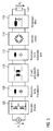
- Fig. 1 The basic subdivision of a system for inductive energy transfer is in Fig. 1 shown.
- Core component in the case of contactless, inductive energy transfer is a loosely coupled transformer, which represents the magnetic coupling of a coil in the base part 102 with a coil in the handset 104 on circuitry level.
- the energy transfer between base and handset takes place.
- this energy can be used to enable the functionality of the handset, on the other hand it can be used in accumulators (for modern applications mostly Li-Lonen batteries, but there are also other types of batteries such as lead, NiCd, NiMh).
- Types etc. can be temporarily stored. Will the handset 104 as in Fig. 1 (b) shown removed from the base station 102, the energy transfer is interrupted. The handset 104 is then powered from the previously charged internal energy storage or dwells in an inactive state until the next contact with the base 102.
- the most well-known example of such an inductive charging system is the electric toothbrush, which makes it possible to charge the toothbrush as a mobile part 104 without a galvanic connection.
- the current state of the art in the application of IE usually includes a signal feedback between power sink and source, whereby the current electrical state of the galvanically isolated secondary side on the primary side is known in any form.
- This information is used on the primary side to respond to a change in the secondary load by changing a manipulated variable (switching frequency, duty cycle, etc.) on the primary side.
- This technical approach requires the provision of a channel to transmit this information.
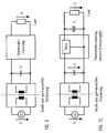
- Known technical realizations, eg DE 3902618 A1 . DE 101 58 794 B4 . US Pat. No. 6,912,137 B2 use a separate physical channel for this signal feedback, as shown in Fig. 2 is shown.
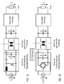
- the basic structure of the power section of a system based on a resonant DC-DC converter for IE is in Fig. 5 shown.
- This type of converter is to be considered in the context of inductive energy transmission as prior art.
- other converter types based on a transformer are conceivable (flyback, forward, Cuk, asymmetric half-bridge, etc.).
- the input voltage V is chopped by a switch bridge 106 into a high-frequency AC voltage.
- This switch bridge 106 may consist of a full or half bridge, wherein semiconductor switches are used as active components.
- This AC voltage is applied to the primary side of the loosely coupled transformer 110.
- blind elements which are shown schematically as resonant circuits 108 and 112.
- a series capacitance is inserted on the primary side, but it is also possible to provide a plurality of reactive elements for selectively influencing the frequency characteristics of the primary circuit.
- LLC additional reactive elements
- LLCC main inductance of the transformer
- the secondary current is rectified on the output side.
- the rectification 114 can be designed as full-wave or half-wave rectification, as components both regular diodes and semiconductor switches can be used (synchronous rectification).
- the rectified output current is smoothed by means of a filter 116 (inductance optional).
- the current state of the art uses a feedback signal to realize a desired-actual-value comparison by z. B. in the case of the resonant converter track the switching frequency as a manipulated variable of the controlled system.
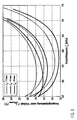
- a change in the output load is also a change in the output load, if the switching frequency is selected as a fixed value, as from the intersection of the dashed curves Fig. 6 evident. Accordingly, this special operating point can only be used to a very limited extent from the point of view of as constant an output voltage as possible. In particular, a direct supply of sensitive loads with a very narrow range of values of the permissible load voltage with a fixed selection of the switching frequency is thus impossible.
- the efficiency of the IE system in this area is very sensitive to distance variations.
- the positioning is severely limited in systems utilizing the coupling-independent point and care must be taken under efficiency aspects that not too large distance variations from the nominal distance are possible.
- the present invention is based on the idea of eliminating signal feedback by dropping the requirement of a stabilized output voltage.
- the resonant stage is operated fixed frequency, the choice of the switching frequency in contrast to previously known approaches can in principle be arbitrary. With regard to minimum losses, however, there is an excellent optimum for this parameter, see also the above statements.
- the free choice of the switching frequency therefore simplifies the design of the resonant converter stage considerably. Moreover, this approach allows a targeted optimal design of this stage.
- the present invention proposes an extension to a two-stage concept.
- the second stage of the preparation of the secondary-side output voltage V o is used .
- the block diagram of such post-stabilization is in Fig. 9 shown.
- the present invention advantageously makes it possible completely to dispense with a separate signal feedback in order to make the construction of the magnetic coupling between primary and secondary side technically as simple as possible.
- the design can be made with the highest possible priority on the energy transfer and there must be no technical compromises or complex demodulation circuits are taken into account.
- the resonant LLC converter is used only to ensure the ZVS operation of the so-called " electronic transformer” .
- no classical transformer is used, in which the air gap between quasi zero and a maximum value can be fixed. Rather, it is loosely coupled coils, which can only be approximated to a minimum distance. This is not adjustable to any small value. Accordingly, as a developer of a system for inductive energy transmission system-related with a, even under optimal conditions, very low magnetizing inductance L m and a very high leakage inductance L res to fight.
- the present invention therefore proposes a circuit for a system for contactless, inductive energy transmission, in particular for use in the power supply of mobile devices.
- a primary-side circuit is arranged on a primary side and can be connected to a primary-side supply voltage
- a secondary-side circuit is arranged on a secondary side and can be connected to a load to be supplied with energy.
- a galvanically isolated transmitter stage for contactlessly transferring energy from the primary side across an air gap to the secondary, wherein at least two magnetically coupled inductive energy transfer coils are provided, which are physically separable by removing the secondary from the primary side are.
- the transformer stage has a resonant converter and the secondary-side circuit further comprises a Nachstabilmaschineseck.
- the Nachstabilmaschinestress according to the present invention may be designed as a simple linear regulator or as a switched mode power supply, as shown in Fig. 10 and Fig. 11 is shown. Moreover, an even simpler overvoltage limitation as the only "voltage control" is conceivable. Both the linear regulator and the switching power supply for restabilization can be implemented as an integrated module or constructed from discrete components.
- the buck converter For the use of a clocked power supply for the Nachstabilmaschine come a variety of DC-DC converters in question, in particular in this context, the buck converter, the buck-boost converter, the Cuk converter and the boost converter called. It is also possible to use galvanically separated converters, such as the flyback or forward converter, as well as load-resonant or switch-resonant converters. For very insensitive loads, only a simple overvoltage limitation can be provided.
- the overcoming of the air gap can preferably take place, among other realizations already mentioned, with the aid of resonant converters, as shown in FIG Fig. 5 is shown.
- the parasitic properties of the loosely coupled transformer can be compensated. Both on the primary side and on the secondary side, a series or parallel compensation can be performed (capacitor). On the secondary side, this compensation can also be omitted.
- other reactive elements can also be provided for selectively influencing the frequency characteristics of the resonant circuit.
- this DC voltage can be provided directly by a battery or by a DC-DC converter, as in Fig. 14 and Fig. 15 shown.
- boost converters which are illustrated by way of example can also use different DC-DC converters (Buck, Buck Boost, Flyback, Forward, Cuk, etc.). Is the input voltage V; as a DC voltage system-conditioned not available from the outset, it must first from another source voltage, as in Fig. 15 illustrated, processed. Accordingly, the proposed concept of a two-stage overcoming of the air gap usually requires a third stage for conditioning the input voltage.
- the DC voltage V g can also be generated by rectifying the mains voltage by means of a bridge rectifier with storage capacitor.
- the rectified and smoothed line voltage in this case serves as the input voltage of a DC-DC converter, which compensates for the resulting ripple (double mains frequency) and provides a stabilized output voltage.
- This stabilized DC voltage in turn serves the converter stage to overcome the air gap as an input voltage.
- boost converter also any other topologies such.
- the buck converter can be used.
- a passive power factor correction can be provided (smoothing reactor).
- an active power factor correction may be made to generate V i .
- the resonant intermediate can also be supplied directly from a rectified alternating network, as in Fig. 17 shown schematically.
- This in turn operates as a fixed frequency electronic transformer and additionally improves the network-side power factor compared to a rectifier bridge in combination with a storage capacitor.
- the illustrated capacitor C HF has a small nominal value.
- a storage capacitor electrolytic capacitor
- it can not buffer significant energy, but only serves to filter the high-frequency harmonics of the input current of the converter stage to overcome the air gap.
- a voltage ripple arises on the output voltage V o at twice the line frequency.
- this residual ripple is again compensated by the post-stabilization stage on the secondary side.
- Resonant converters were identified as the favored topology for overcoming the air gap.
- Preferred basic structures of the resonant circuits are in the FIGS. 18 to 20 shown.
- the structure of the resonant circuit of the resonant converter differs by the presence and placement of a capacitor on the secondary side.
- the use of a full bridge for rectification is advantageous, otherwise the secondary side can also be used as center tap (see Fig. 19 ) to minimize the diode losses that occur.
- the post-stabilization is in Fig. 18 realized by a buck converter.
- a buck-boost converter was selected as the topology for restabilization.
- a boost converter as in Fig. 20 shown, can be used.
- the post-stabilization stage is realized by way of example by means of a buck converter, but as already mentioned, different variants of the post-stabilization can be used. Likewise, different resonant circuit topologies are possible.
- Fig. 21 the processing of the input-side mains voltage takes place with the aid of a simple rectifier bridge in conjunction with a storage capacitor. This smoothes the rectified mains voltage and charges in a first approximation to the peak value of the mains voltage.
- the resulting voltage ripple of the secondary-side output voltage V o of the resonant stage is regulated (in addition to the voltage variation due to different positional relationships) by the post-stabilization stage.
- a passive power factor correction can be provided as described in Fig. 22 is shown schematically.
- the recharging pulses are widened by additional impedances (usually inductive), whereby the recorded distortion reactive power decreases and the power factor increases.
- the smoothing inductor L PFC is used in particular for the passive PFC .
- a boost converter was chosen by way of example.
Landscapes
- Engineering & Computer Science (AREA)
- Power Engineering (AREA)
- Computer Networks & Wireless Communication (AREA)
- Signal Processing (AREA)
- Dc-Dc Converters (AREA)
- Charge And Discharge Circuits For Batteries Or The Like (AREA)
- Secondary Cells (AREA)
Abstract
Description
Die vorliegende Erfindung bezieht sich auf eine Schaltung für ein System zur kontaktlosen, induktiven Energieübertragung, insbesondere zur Anwendung bei der Energieversorgung mobiler Geräte sowie auf eine zugehörige Ladeschaltung.The present invention relates to a circuit for a system for contactless, inductive power transmission, in particular for use in the power supply of mobile devices and to an associated charging circuit.
Das Prinzip der induktiven Energieübertragung dient in einer Vielzahl von Applikationen als physikalische Grundlage zur technischen Erschließung eines weiten Applikationsbereichs. Die prinzipielle Unterteilung eines Systems zur induktiven Energieübertragung ist in
Durch die räumliche Anordnung des Mobilteils 104 in der Nähe des Basisteils 102 wird der Energietransfer zwischen Basis- und Mobilteil ermöglicht. Als bekanntestes Beispiel eines solchen induktiven Ladesystems ist die elektrische Zahnbürste zu nennen, welche das Laden der Zahnbürste als Mobilteil 104 ohne galvanische Verbindung ermöglicht.The spatial arrangement of the
Der Verzicht auf galvanische Leitungen ist für eine große Zahl an Anwendungsszenarien von sehr großer Bedeutung. Insbesondere trifft dies auf Anwendungen mit hohen Ansprüchen an den mechanischen Aufbau der elektrischen Verbindungen zwischen Leistungsquelle und -senke zu, bei denen technisch komplexe Stecker und Kabel durch die Verwendung der induktiven Energieübertragung (IE) vermieden werden können. Darüber hinaus können technische Energieversorgungssystemkomponenten basierend auf IE vor Umwelteinflüssen geschützt werden, ohne dass herausgeführte Steckverbinder den mechanischen Aufbau unnötig kompliziert machen. Überdies existieren Einsatzgebiete der IE, bei denen der Einsatz von galvanischen Verbindungen im Hinblick auf eine technische Realisierbarkeit vermieden werden muss, z. B. in explosionsgefährdeten Umgebungen oder beim Betrieb der Systemkomponenten in leitfähigen und/oder aggressiven Medien. Ferner kann der Einsatz der IE die Zuverlässigkeit technischer Systeme erhöhen. Dies ist zum einen bei Systemen mit rotierenden oder beweglichen Teilen der Fall, da dort auf verschleißanfällige Schleifkontakte verzichtet werden kann, zum anderen bei Geräten mit Steckverbindern, die ansonsten für eine hohe Anzahl an Steckspielen ausgelegt werden müssten.The absence of galvanic lines is very important for a large number of application scenarios. In particular, this applies to applications with high demands on the mechanical structure of the electrical connections between the power source and sink, in which technically complex plug and cable can be avoided by the use of inductive energy transfer (IE). In addition, technical power supply system components based on IE can be protected from environmental influences without the connectors being brought out of the mechanical structure unnecessarily complicated. Moreover, there are areas of application of IE, in which the use of galvanic connections must be avoided in terms of technical feasibility, z. In potentially explosive environments or when operating the system components in conductive and / or aggressive media. Furthermore, the use of IE can increase the reliability of technical systems. This is on the one hand in systems with rotating or moving parts of the case, since there can be dispensed with wear-prone sliding contacts, on the other hand with devices with connectors that would otherwise have to be designed for a high number of plug-in games.
Im Zusammenhang mit der zunehmenden Marktdurchdringung technischer Lösungen basierend auf dem Prinzip der IE muss auch der Aspekt der Nutzerfreundlichkeit hervorgehoben werden. Insbesondere im Bereich tragbarer elektrischer Leistungssenken wird dieser Mehrwert für den Nutzer durch die vereinfachte Handhabung deutlich, der die Versorgung dieser tragbaren Geräte einzig durch Platzierung des Mobilteils an der Ladestation initiieren kann.In the context of increasing market penetration of technical solutions based on the IE principle, the user-friendliness aspect must also be emphasized. Especially in the field of portable electric power sinks this added value for the user through the simplified handling is clear, which can initiate the supply of these portable devices only by placing the handset to the charging station.
Der aktuelle Stand der Technik beinhaltet bei der Anwendung der IE meist eine Signalrückführung zwischen Leistungssenke und -quelle, wodurch der aktuelle elektrische Zustand der galvanisch getrennten Sekundärseite auf der Primärseite in irgendeiner Form bekannt ist. Diese Information wird auf der Primärseite dazu benutzt, durch die Veränderung einer Stellgröße (Schaltfrequenz, Tastgrad, etc.) auf der Primärseite auf eine Veränderung der sekundärseitigen Last zu reagieren. Dieser technische Ansatz erfordert die Bereitstellung eines Kanals zur Übertragung dieser Informationen. Bekannte technische Realisierungen, z.B.
Aus aufbautechnischen Gesichtspunkten heraus ist diese Herangehensweise aufwändig, da sowohl konstruktive Einschränkungen in Kauf genommen werden müssen (Ausrichtung des Mobilteils zum Basisteil kann nur sehr eingeschränkt erfolgen, im Falle der optischen Strecke ist das Herausführen von optischen Bauelementen oder Lichtleitern bzw. Verwendung transparenter Materialien erforderlich, im Falle der separaten magnetischen Kopplung ist ein zweites Spulenpaar unterzubringen) als auch zusätzlicher Bauteil- und Schaltungsaufwand entstehen.From a technical point of view, this approach is costly, since both constructive restrictions must be accepted (alignment of the handset to the base part can be done only very limited, in the case of the optical route is the lead out of optical components or optical fibers or use of transparent materials required, in the case of separate magnetic coupling, a second coil pair is to be accommodated) as well as additional component and circuit complexity arise.
Alternative Ansätze verwenden für die Signalrückführung die gleiche magnetische Kopplung wie für den Energietransport selbst (
Diese bekannte Art der Rückkopplung ist im Hinblick auf die Auslegung der primär- und sekundärseitigen Wicklungen als nachteilig anzusehen, da diese neben dem Energietransport auch für die Übermittlung der Signalinformation ausgelegt werden müssen.This known type of feedback is to be regarded as disadvantageous with regard to the design of the primary and secondary windings, since these must be designed in addition to the energy transport for the transmission of the signal information.
Eine weitere Alternativlösung besteht in der Verwendung von funkgestützten Lösungen (z. B.
Auch diese technische Lösung stellt einen deutlich erhöhten technisch-konstruktiven Aufwand dar. Die für die Bereitstellung des Funkkanals nötigen Komponenten müssen einerseits passend in den Gerätehälften untergebracht werden, insbesondere die Antennen sind passend zueinander zu platzieren. Dadurch ergeben sich beim Betrieb Einschränkungen im Hinblick auf die Ausrichtung der Gerätehälften zueinander. Darüber hinaus erhöht die nachrichtentechnische Aufbereitung des Funksignals den schaltungstechnischen Aufwand.This technical solution represents a significantly increased technical and design effort. The necessary for the provision of the radio channel components must be accommodated on the one hand fit in the device halves, in particular the antennas are to be placed apt to each other. This results in the operation restrictions on the alignment of the device halves to each other. In addition, the telecommunications processing of the radio signal increases the circuitry complexity.
Steht ein Kanal zum Informationsaustausch zwischen Basis- und Mobilteil bereit, so kommen in bestehenden technischen Lösungen unterschiedliche Modulationsverfahren (FM, AM etc.) zum Einsatz. Diese nachrichtentechnische Aufbereitung hat unabhängig von der Art des verwendeten Kanals einen stark erhöhten Anspruch an die technische Realisierung des Systems zur Folge. Dies ist ein zusätzlicher schwerwiegender Nachteil bekannter Lösungen basierend auf der Rückführung eines Signals.If a channel is available for the exchange of information between the base unit and the handset, different modulation methods (FM, AM etc.) are used in existing technical solutions. This telecommunications technology, regardless of the type of channel used to a much higher demands on the technical implementation of the system result. This is an additional serious disadvantage of known solutions based on the feedback of a signal.
Der prinzipielle Aufbau des Leistungsteils eines Systems zur IE auf Basis eines resonanten DC-DC-Konverters ist in
Auf der Sekundärseite kann auf den Einsatz zusätzlicher Blindelemente verzichtet werden (LLC), es können aber auch Kapazitäten zur Kompensation der Hauptinduktivität des Übertragers eingesetzt werden (LLCC), sowohl in Parallel- als auch in Serienschaltung. Darüber hinaus ist auch der Einsatz von zusätzlichen Blindelementen möglich, wiederum zur gezielten Beeinflussung der Frequenzeigenschaften der Sekundärseite.On the secondary side can be dispensed with the use of additional reactive elements (LLC), but it can also be used to compensate for the main inductance of the transformer (LLCC), both in parallel and in series. In addition, the use of additional reactive elements is possible, in turn, for selectively influencing the frequency characteristics of the secondary side.
Der Sekundärstrom wird auf der Ausgangsseite gleichgerichtet. Die Gleichrichtung 114 kann als Vollweg- oder Halbweggleichrichtung ausgeführt sein, als Bauelemente können sowohl reguläre Dioden als auch Halbleiterschalter eingesetzt werden (Synchrongleichrichtung). Der gleichgerichtete Ausgangsstrom wird mit Hilfe eines Filters 116 (Induktivität optional) geglättet.The secondary current is rectified on the output side. The
Der aktuelle Stand der Technik nutzt ein zurückgeführtes Signal zur Realisierung eines Soll-Ist-Wert-Vergleichs um z. B. im Falle des resonanten Konverters die Schaltfrequenz als Stellgröße des geregelten Systems nachzuführen.The current state of the art uses a feedback signal to realize a desired-actual-value comparison by z. B. in the case of the resonant converter track the switching frequency as a manipulated variable of the controlled system.
Es existieren aber auch technische Ansätze, die den Verzicht der Signalrückführung im Falle resonanter Konverter durch eine eingeschränkte Wahl des Arbeitspunktes ermöglichen sollen. Diese basieren auf der Festlegung der Schaltfrequenz auf einen festen Wert. Um bei diesen Ansätzen die Variation der Ausgangsspannung bei unterschiedlichen Kopplungsverhältnissen zu begrenzen, wird der Betrieb am so genannten "coupling independent point" vorgeschlagen, einem Arbeitspunkt, bei dem sich bei gleicher resistiver Belastung des Ausgangs in etwa die gleiche Ausgangsspannung einstellt.But there are also technical approaches that should allow the waiver of the signal feedback in the case of resonant converter by a limited choice of the operating point. These are based on the determination of the switching frequency to a fixed value. In order to limit the variation of the output voltage at different coupling ratios in these approaches, the operation is proposed at the so-called "coupling independent point", an operating point at which the same output voltage is established for the same resistive load of the output.
Oftmals basieren diese ermittelten ausgezeichneten Arbeitspunkte auf vereinfachten Berechnungsmethoden. Analysiert man hingegen die sich einstellende Ausgangsspannung unter Belastung für verschiedene Abstände eines Systems zur IE genauer, so erhält man die in
Wie aus diesen Verläufen ersichtlich wird, ist diese charakteristische Eigenschaft eines kopplungsunabhängigen Punktes für das dargestellte, exemplarisch ausgewählte System zwar nachvollziehbar (Wahl der Schaltfrequenz bei fs ≈ 48 kHz für IG = 3 und IG = 6 mm), in einem praktischen System aber nur unter sehr starken Einschränkungen nutzbar. So ist direkt ersichtlich, dass für schlechte Kopplungsverhältnisse, im gewählten Beispiel für IG = 8 mm, die Eigenschaft einer möglichst konstanten Ausgangsspannung verloren geht. Darüber hinaus ergibt sich zwangsläufig eine Variation des Ausgangsspannungswertes, wenn der Ausgang mit einer von der Nennleistung verschiedenen Leistung belastet wird, insbesondere im Falle des Leerlaufs, der bei fast jeder Applikation vorkommt.As can be seen from these courses, this characteristic property of a coupling-independent point for the illustrated exemplarily selected system is understandable (choice of switching frequency at f s ≈ 48 kHz for I G = 3 and I G = 6 mm), in a practical system but usable only under very strong restrictions. Thus it can be seen directly that for poor coupling ratios, in the example chosen for I G = 8 mm, the property of the most constant possible output voltage is lost. In addition, a variation of the output voltage value inevitably results when the output is loaded with power different from the rated power, especially in the case of idling, which occurs in almost every application.
Durch die Verwendung der in den folgenden Ausführungen beschriebenen erfindungsgemäßen Idee werden mehrere Probleme im Hinblick auf die technische Realisierung eines Systems zur IE beseitigt. Bei Verwendung eines Rückführsignals muss der zugehörige Signalpfad entweder separat realisiert oder mit großem Einfluss auf die Auslegung der magnetischen Kopplung im Hauptenergieflusspfad integriert werden. Beide Lösungen haben deutlich erhöhten technischen Aufwand zur Folge. Bei Verwendung der hier beschriebenen Idee kann somit durch den Verzicht auf eine Signalrückführung für eine bestmögliche mechanische und elektrische Auslegung des Gesamtsystems im Hinblick auf die Energieübertragung gesorgt werden.By using the inventive idea described in the following embodiments, several problems with regard to the technical realization of a system for IE are eliminated. When using a feedback signal, the associated signal path must either be realized separately or integrated with great influence on the design of the magnetic coupling in the main energy flow path. Both solutions have significantly increased technical complexity result. By using the idea described here, it is thus possible, by dispensing with signal feedback, to ensure the best possible mechanical and electrical design of the overall system in terms of energy transmission.
Ein weiteres technisches Problem ergibt sich aus der Ausnutzung des kopplungsunabhängigen Arbeitspunktes. Zum einen lässt sich für das gewählte Beispiel aus
Zum anderen stellt sich bei Veränderung der Ausgangslast ebenfalls eine Änderung der Ausgangsspannung ein, falls die Schaltfrequenz als fixer Wert gewählt wird, wie aus dem Schnittpunkt der gestrichelten Verläufe aus
Betrachtet man neben der Ausgangsspannungsvariation einen weiteren wichtigen Gesichtspunkt eines festfrequent betriebenen Systems zur IE, nämlich die auftretenden Verluste aus
Dementsprechend reagiert der Wirkungsgrad des Systems zur IE in diesem Bereich sehr sensitiv auf Abstandsvariationen. Somit ist die Positionierung bei Systemen mit Ausnutzung des kopplungsunabhängigen Punktes stark eingeschränkt und es muss unter Wirkungsgradaspekten darauf geachtet werden, dass keine allzu großen Abstandsvariationen vom Nennabstand möglich sind.Accordingly, the efficiency of the IE system in this area is very sensitive to distance variations. Thus, the positioning is severely limited in systems utilizing the coupling-independent point and care must be taken under efficiency aspects that not too large distance variations from the nominal distance are possible.
Wird hingegen eine Schaltfrequenz im Bereich der Aufsteilung zur Parallelresonanzfrequenz (für dieses exemplarisch gewählte Beispiel bei 65 ... 70 kHz) hin gewählt, so ergeben sich mehrere Vorteile im Hinblick auf die Verlustleistungsentwicklung. Zum einen ist der Absolutwert der auftretenden Verlustleistung in diesem Bereich für die großen Abstände des gezeigten Beispiels am kleinsten. Zum anderen ist die Variation des Wirkungsgrades in diesem Bereich signifikant kleiner. Für die Teillasteffizienz verstärkt sich dieser Effekt nochmals, wie aus
Durch die Einschränkung der möglichen Schaltfrequenz auf die spezielle Lage des kopplungsunabhängigen Arbeitspunktes ergeben sich somit erhebliche Einschränkungen im Hinblick auf die Leistungsfähigkeit des Gesamtsystems, die bei Verwendung der vorliegenden Erfindung aufgehoben werden. Die Ausnutzung des kopplungsunabhängigen Arbeitspunktes hat nichtsdestotrotz eine inhärente Variation der Ausgangsspannung zur Folge. Dieses Vorhandensein einer gewissen Schwankungsbreite der Ausgangsspannung der resonanten Stufe erfüllt die Anforderungen an die notwendige Stabilität der Ausgangsspannung für die Versorgung moderner leistungselektronischer Lasten nicht. Somit ist die Ausnutzung des "coupling indepedent point" nur bei einer sehr eingeschränkten Klasse von Energieverbrauchern auf der Sekundärseite möglich. Bei modernen Anwendungsszenarien wird dagegen selbst bei Verwendung dieses ausgezeichneten Arbeitspunktes die Spannungsvariation der Versorgungsspannung dieser Lasten unzulässig groß. Nicht zuletzt bei Ladeapplikationen basierend auf Li-lonen-Technik muss dieser Variation aber Rechnung getragen werden.Limiting the possible switching frequency to the specific position of the coupling-independent operating point thus results in considerable restrictions with regard to the performance of the overall system, which are eliminated when using the present invention. The utilization of the coupling-independent operating point nonetheless results in an inherent variation of the output voltage. This presence of a certain fluctuation of the output voltage of the resonant stage does not meet the requirements for the necessary stability of the output voltage for the supply of modern power electronics loads. Thus, the utilization of the "coupling indepedent point" is only possible with a very limited class of energy consumers on the secondary side. In modern application scenarios, however, even when using this excellent operating point, the voltage variation of the supply voltage of these loads becomes unacceptably large. Not least with Charge applications based on Li-ion technology, however, must be taken into account for this variation.
Daher basiert die vorliegende Erfindung auf der Idee, auf eine Signalrückführung zu verzichten, indem die Forderung einer stabilisierten Ausgangsspannung fallengelassen wird. Die resonante Stufe wird dabei festfrequent betrieben, wobei die Wahl der Schaltfrequenz im Gegensatz zu bisher bekannten Ansätzen prinzipiell beliebig erfolgen kann. Im Hinblick auf minimale Verluste gibt es aber für diesen Parameter ein ausgezeichnetes Optimum, siehe hierzu auch die obigen Ausführungen. Die freie Wahl der Schaltfrequenz vereinfacht daher den Aufbau der resonanten Wandlerstufe erheblich. Überdies ermöglicht dieser Ansatz eine gezielte optimale Auslegung dieser Stufe.Therefore, the present invention is based on the idea of eliminating signal feedback by dropping the requirement of a stabilized output voltage. The resonant stage is operated fixed frequency, the choice of the switching frequency in contrast to previously known approaches can in principle be arbitrary. With regard to minimum losses, however, there is an excellent optimum for this parameter, see also the above statements. The free choice of the switching frequency therefore simplifies the design of the resonant converter stage considerably. Moreover, this approach allows a targeted optimal design of this stage.
Damit trotzdem empfindliche Lasten auf der Sekundärseite versorgt werden können, schlägt die vorliegende Erfindung eine Erweiterung auf ein zweistufiges Konzept vor. Dabei dient die zweite Stufe der Aufbereitung der sekundärseitigen Ausgangsspannung Vo. Das Blockschaltbild einer solchen Nachstabilisierung ist in
Die vorliegende Erfindung ermöglicht in vorteilhafter Weise, komplett auf eine gesonderte Signalrückführung zu verzichten, um den Aufbau der magnetischen Kopplung zwischen Primär- und Sekundärseite technisch so einfach wie möglich zu gestalten. Somit kann die Auslegung mit größtmöglicher Priorität auf die Energieübertragung erfolgen und es müssen keine technischen Kompromisse eingegangen oder aufwändige Demodulationsschaltungen berücksichtigt werden.The present invention advantageously makes it possible completely to dispense with a separate signal feedback in order to make the construction of the magnetic coupling between primary and secondary side technically as simple as possible. Thus, the design can be made with the highest possible priority on the energy transfer and there must be no technical compromises or complex demodulation circuits are taken into account.
Aus der Dissertation
Der in dieser Dissertation diskutierte Ansatz eines dreistufigen Schaltnetzteils verfolgt den Ansatz, Probleme bei der Auslegung eines klassischen Schaltnetzteils (SNT) mit zwei Stufen durch Hinzunahme einer dritten Stufe zu überwinden. Hierbei wird insbesondere der Zusammenhang zwischen der Größe des Zwischenkreis-Elektrolytkondensators für die Einhaltung einer gewissen Verweilzeit und dem nötigen Eingangsspannungsbereich der DC-DC Stufe betrachtet. Darüber hinaus ist es im Allgemeinen für die Effizienz eines DC-DC-Konverters eher von Nachteil, wenn dieser einen hohen Eingangsspannungsbereich abdecken muss, da diese Anforderung weitreichende Einschränkungen bei dessen Auslegung mit sich bringt.The approach of a three-stage switched-mode power supply discussed in this thesis pursues the approach of overcoming problems with the design of a conventional two-stage switching power supply (SNT) by adding a third stage. In particular, the relationship between the size of the DC link electrolytic capacitor for maintaining a certain residence time and the required input voltage range of the DC-DC stage is considered. Moreover, it is generally more disadvantageous for the efficiency of a DC-DC converter if it covers a high input voltage range because this requirement entails far-reaching limitations in its interpretation.
Im Gegensatz zu der vorliegenden Problemstellung findet der resonante LLC-Konverter nur zur Sicherstellung des ZVS-Betriebs des so genannten "electronic transformers" Verwendung. Bei der Applikation der induktiven Energieübertragung hingegen kommt kein klassischer Transformator zum Einsatz, bei dem der Luftspalt zwischen quasi Null und einem Maximalwert fest eingestellt werden kann. Vielmehr handelt es sich um lose gekoppelte Spulen, welche nur bis auf einen Minimalabstand angenähert werden können. Dieser ist nicht auf einen beliebig kleinen Wert einstellbar. Dementsprechend hat man als Entwickler eines Systems zur induktiven Energieübertragung systembedingt mit einer, selbst unter Optimalbedingungen, sehr niedrigen Magnetisierungsinduktivität Lm sowie einer sehr hohen Streuinduktivität L res zu kämpfen. Überdies ergeben sich durch mechanische Toleranzen bei der Herstellung der Geräteteile sowie bei deren Positionierung zueinander variable Abstände selbst im Betrieb, während der Luftspalt aus der Dissertation Schwalbe einen fixen Wert darstellt, welcher in der Designphase gezielt gewählt werden kann. Für die Applikation der induktiven Energieübertragung hat dies zur Folge, dass nur Topologien sinnvoll einsetzbar sind, welche mit stark variierenden Zuständen der losen magnetischen Kopplung zurecht kommen. Eine solche Topologie ist z. B. der resonante LLCC-Konverter.In contrast to the present problem, the resonant LLC converter is used only to ensure the ZVS operation of the so-called " electronic transformer" . In the application of inductive energy transmission, however, no classical transformer is used, in which the air gap between quasi zero and a maximum value can be fixed. Rather, it is loosely coupled coils, which can only be approximated to a minimum distance. This is not adjustable to any small value. Accordingly, as a developer of a system for inductive energy transmission system-related with a, even under optimal conditions, very low magnetizing inductance L m and a very high leakage inductance L res to fight. Moreover, resulting from mechanical tolerances in the manufacture of the device parts and their positioning mutually variable distances even during operation, while the air gap from the dissertation Schwalbe represents a fixed value, which can be selected specifically in the design phase. For the application of inductive energy transmission, this has the consequence that only topologies can be usefully used, which cope with greatly varying states of loose magnetic coupling. Such a topology is z. B. the resonant LLCC converter.
Die vorliegende Erfindung schlägt daher eine Schaltung für ein System zur kontaktlosen, induktiven Energieübertragung vor, insbesondere zur Anwendung bei der Energieversorgung mobiler Geräte. Eine primärseitige Schaltung ist auf einer Primärseite angeordnet und ist mit einer primärseitigen Versorgungsspannung verbindbar, und eine sekundärseitige Schaltung ist auf einer Sekundärseite angeordnet und mit einer mit Energie zu versorgenden Last verbindbar.The present invention therefore proposes a circuit for a system for contactless, inductive energy transmission, in particular for use in the power supply of mobile devices. A primary-side circuit is arranged on a primary side and can be connected to a primary-side supply voltage, and a secondary-side circuit is arranged on a secondary side and can be connected to a load to be supplied with energy.
Gemäß der vorliegenden Erfindung ist eine Übertragerstufe mit galvanischer Trennung zum kontaktlosen Übertragen von Energie von der Primärseite über einen Luftspalt hinweg auf die Sekundärseite vorgesehen, wobei mindestens zwei magnetisch gekoppelte Spulen zur induktiven Energieübertragung vorgesehen sind, die durch Entfernen der Sekundärseite von der Primärseite räumlich voneinander trennbar sind. Die Übertragerstufe weist einen resonanten Wandler auf und die sekundärseitige Schaltung umfasst weiterhin eine Nachstabilisierungsstufe.In accordance with the present invention, a galvanically isolated transmitter stage is provided for contactlessly transferring energy from the primary side across an air gap to the secondary, wherein at least two magnetically coupled inductive energy transfer coils are provided, which are physically separable by removing the secondary from the primary side are. The transformer stage has a resonant converter and the secondary-side circuit further comprises a Nachstabilisierungsstufe.
Die Nachstabilisierungsstufe gemäß der vorliegenden Erfindung kann als einfacher Linearregler oder als getaktetes Schaltnetzteil ausgeführt sein, wie dies in
Zum besseren Verständnis der vorliegenden Erfindung wird diese anhand der in den nachfolgenden Figuren dargestellten Ausführungsbeispiele näher erläutert. Dabei werden gleiche Teile mit gleichen Bezugszeichen und gleichen Bauteilbezeichnungen versehen. Weiterhin können auch einzelne Merkmale oder Merkmalskombinationen aus den gezeigten und beschriebenen Ausführungsformen für sich genommen eigenständige erfinderische oder erfindungsgemäße Lösungen darstellen.For a better understanding of the present invention, this will be explained in more detail with reference to the embodiments illustrated in the following figures. The same parts are provided with the same reference numerals and the same component names. Furthermore, individual features or combinations of features from the embodiments shown and described can in themselves represent independent inventive or inventive solutions.
Es zeigen:
- Fig. 1
- eine schematische Darstellung der prinzipiellen Unterteilung eines Systems zur induktiven Energieübertragung;
- Fig. 2
- eine schematische Darstellung des Informationsaustausches zwischen einem Basis- und einem Mobilteil über einen separat bereitgestellten Informationskanal;
- Fig. 3
- eine schematische Darstellung des Informationsaustausches zwischen Basisteil und Mobilteil über dieselbe magnetische Kopplung wie für den Energietransport selbst;
- Fig. 4
- eine schematische Darstellung des Informationsaustausches zwischen einem Basis- und einem Mobilteil über Funk;
- Fig. 5
- eine schematische Darstellung des prinzipiellen Aufbaus eines Systems zur induktiven Energieübertragung auf der Basis eines resonanten DC-DC-Konverters;
- Fig. 6
- simulierte Verläufe der Ausgangsspannung eines Systems zur IE auf Basis eines LLCC-Konverters für verschiedene Abstände der Gerätehälften bei Belastung des Ausgangs mit Nennleistung als Funktion der Schaltfrequenz (durchgezogene Linie: Ausgangsspannung unter Belastung mit Nennausgangsleistung, gestrichelte Linie: Ausgangsspannung im Leerlauf);
- Fig. 7
- simulierte Verläufe der Verlustleistung eines Systems zur IE auf Basis eines LLCC-Konverters für verschiedene Abstände der Gerätehälften bei Belastung des Ausgangs mit Nennleistung als Funktion der Schaltfrequenz;
- Fig. 8
- simulierte Verläufe der Verlustleistung eines Systems zur IE auf Basis eines LLCC-Konverters für verschiedene Abstände der Gerätehälften bei Belastung des
Ausgangs mit 20% der Nennleistung als Funktion der Schaltfrequenz; - Fig. 9
- eine schematische Darstellung einer zweistufigen Systemstruktur gemäß der vorliegenden Erfindung;
- Fig. 10
- eine schematische Darstellung einer Schaltungsanordnung mit einer Nachstabilisierungsstufe basierend auf einem Linearregler;
- Fig. 11
- eine schematische Darstellung einer Schaltungsanordnung mit einer Nachstabilisierungsstufe basierend auf einem Schaltnetzteil mit einem Buck-Konverter;
- Fig. 12
- eine schematische Darstellung einer Schaltungsanordnung, bei welcher der Luftspalt mit Hilfe eines Flyback-Konverters überwunden wird;
- Fig. 13
- eine schematische Darstellung einer Schaltungsanordnung, bei der der Luftspalt mit Hilfe eines Forward-Konverters überwunden wird;
- Fig. 14
- eine schematische Darstellung einer Schaltungsanordnung, bei welcher die potentialgetrennte Stufe aus einer Batterie versorgt wird;
- Fig. 15
- eine schematische Darstellung einer Schaltungsanordnung, bei der die potentialgetrennte Stufe mittels eines Hochsetzstellers versorgt wird;
- Fig. 16
- eine schematische Darstellung einer Schaltungsanordnung, bei der die Eingangsspannung der potentialgetrennten Stufe mit Hilfe eines Gleichrichters aufbereitet wird;
- Fig. 17
- eine schematische Darstellung einer Schaltungsanordnung, bei der die potentialge-trennte Stufe als "electronic transformer" zur IE betrieben wird und diese gleichzei-tig den netzseitigen Leistungsfaktor anhebt;
- Fig. 18
- eine schematische Darstellung einer Schaltungsanordnung gemäß einer vorteilhaften Ausführungsform, bei der die potentialgetrennte Stufe mittels eines resonanten LLCC-Konverters realisiert ist und die Nachstabilisierung mit Hilfe eines Buck-Konverters erfolgt;
- Fig. 19
- eine schematische Darstellung einer Schaltungsanordnung gemäß einer weiteren vorteilhaften Ausführungsform, bei der die potentialgetrennte Stufe mittels eines resonanten LLC-Konverters und einer Mittelpunktsanzapfung auf der Sekundärseite realisiert wird und die Nachstabilisierung mit Hilfe eines Buck-Boost-Konverters erfolgt;
- Fig. 20
- eine schematische Darstellung einer Schaltungsanordnung gemäß einer weiteren vorteilhaften Ausführungsform, bei der die potentialgetrennte Stufe mittels eines resonanten LLCC-Konverters ausgeführt ist und die Nachstabilisierung mit Hilfe eines Boost-Konverters erfolgt;
- Fig. 21
- eine schematische Darstellung einer Schaltungsanordnung, bei der die Eingangsspannung der potentialgetrennten Stufe mit Hilfe eines Gleichrichters und eines Speicherkondensators bereitgestellt wird;
- Fig. 22
- eine schematische Darstellung einer Schaltungsanordnung, bei der die Eingangsspannung der potentialgetrennten Stufe mit Hilfe einer passiven Leistungsfaktorkorrektur bereitgestellt wird;
- Fig. 23
- eine schematische Darstellung einer Schaltungsanordnung, bei der die Eingangsspannung der potentialgetrennten Stufe mit Hilfe eines DC-DC-Konverters bereitgestellt wird;
- Fig. 24
- eine schematische Darstellung einer Schaltungsanordnung, bei der die Eingangsspannung der potentialgetrennten Stufe mit Hilfe einer aktiven Leistungsfaktorkorrekturschaltung bereitgestellt wird.
- Fig. 1
- a schematic representation of the basic division of a system for inductive energy transfer;
- Fig. 2
- a schematic representation of the information exchange between a base and a handset over a separately provided information channel;
- Fig. 3
- a schematic representation of the information exchange between base and handset over the same magnetic coupling as for the energy transport itself;
- Fig. 4
- a schematic representation of the information exchange between a base and a handset via radio;
- Fig. 5
- a schematic representation of the basic structure of a system for inductive energy transmission on the basis of a resonant DC-DC converter;
- Fig. 6
- simulated output voltage curves of a system for IE based on an LLCC converter for different distances between the halves of the device when the output is rated at rated power as a function of switching frequency (solid line: output voltage under load at rated output power, dashed line: output voltage at no load);
- Fig. 7
- simulated loss of power of a system for IE based on an LLCC converter for different distances between the halves of the device when the output is loaded with nominal power as a function of the switching frequency;
- Fig. 8
- simulated loss of power of a system based on an LLCC converter for different distances of the halves of the device when the output is loaded with 20% of the nominal power as a function of the switching frequency;
- Fig. 9
- a schematic representation of a two-stage system structure according to the present invention;
- Fig. 10
- a schematic representation of a circuit arrangement with a Nachstabilisierungsstufe based on a linear regulator;
- Fig. 11
- a schematic representation of a circuit arrangement with a Nachstabilisierungsstufe based on a switching power supply with a buck converter;
- Fig. 12
- a schematic representation of a circuit arrangement in which the air gap is overcome by means of a flyback converter;
- Fig. 13
- a schematic representation of a circuit arrangement in which the air gap is overcome by means of a forward converter;
- Fig. 14
- a schematic representation of a circuit arrangement in which the floating stage is powered by a battery;
- Fig. 15
- a schematic representation of a circuit arrangement in which the potential-separated stage is supplied by means of a boost converter;
- Fig. 16
- a schematic representation of a circuit arrangement in which the input voltage of the floating stage is prepared by means of a rectifier;
- Fig. 17
- a schematic representation of a circuit arrangement in which the potential-separated stage is operated as an "electronic transformer" to IE and this at the same time raises the network-side power factor;
- Fig. 18
- a schematic representation of a circuit arrangement according to an advantageous embodiment, in which the potential-separated stage is realized by means of a resonant LLCC converter and the Nachstabilisierung using a buck converter;
- Fig. 19
- a schematic representation of a circuit arrangement according to a further advantageous embodiment, in which the floating stage is realized by means of a resonant LLC converter and a center tap on the secondary side and the Nachstabilisierung using a buck-boost converter;
- Fig. 20
- a schematic representation of a circuit arrangement according to a further advantageous embodiment, in which the potential-separated stage is carried out by means of a resonant LLCC converter and the Nachstabilisierung takes place by means of a boost converter;
- Fig. 21
- a schematic representation of a circuit arrangement in which the input voltage of the floating stage is provided by means of a rectifier and a storage capacitor;
- Fig. 22
- a schematic representation of a circuit arrangement in which the input voltage of the floating stage is provided by means of a passive power factor correction;
- Fig. 23
- a schematic representation of a circuit arrangement in which the input voltage of the floating stage is provided by means of a DC-DC converter;
- Fig. 24
- a schematic representation of a circuit arrangement in which the input voltage of the floating stage is provided by means of an active power factor correction circuit.
Die vorliegende Erfindung wird nunmehr mit Bezug auf die Figuren im Detail erläutert.The present invention will now be explained in detail with reference to the figures.
Kerngedanke der vorliegenden Erfindung ist die Realisierung eines Systems zur IE basierend auf einem zwei- oder dreistufigen Konzept. Diese Herangehensweise macht die Übermittlung von Informationen zum Zwecke der Regelung der Lastspannung zwischen Primär-und Sekundärseite überflüssig. Dabei sind drei Stufen vorgesehen:
- 1. Stufe:
- Aufbereitung der Eingangsspannung (AC-DC bzw. DC-DC). Je nach Applikation ist diese Stufe optional.
- 2. Stufe:
- Energietransport über einen Luftspalt.
- 3. Stufe:
- Nachstabilisierung.
- 1st stage:
- Preparation of the input voltage (AC-DC or DC-DC). Depending on the application, this level is optional.
- 2nd stage:
- Energy transport via an air gap.
- 3rd stage:
- Poststabilization.
Für den Einsatz eines getakteten Netzteils zur Nachstabilisierung kommen eine Vielzahl von DC-DC-Konvertern in Frage, insbesondere sind in diesem Zusammenhang der Buck-Konverter, der Buck-Boost-Konverter, der Cuk-Konverter sowie der Boost-Konverter genannt. Es können auch galvanisch getrennte Konverter, wie der Flyback- oder Forward-Konverter, sowie lastresonante oder schalterresonante Konverter eingesetzt werden. Für sehr unempfindliche Lasten kann auch nur eine einfache Überspannungsbegrenzung vorgesehen sein.For the use of a clocked power supply for the Nachstabilisierung come a variety of DC-DC converters in question, in particular in this context, the buck converter, the buck-boost converter, the Cuk converter and the boost converter called. It is also possible to use galvanically separated converters, such as the flyback or forward converter, as well as load-resonant or switch-resonant converters. For very insensitive loads, only a simple overvoltage limitation can be provided.
Die Überwindung des Luftspaltes kann vorzugsweise, neben anderen bereits erwähnten Realisierungen, mit Hilfe resonanter Konverter erfolgen, wie dies in
Darüber hinaus sind auch für den Fall der vergleichsweise lose gekoppelten Spulen, welche bei der IE in aller Regel auftreten, auch andere Topologien zur Überwindung des Luftspaltes denkbar. So könnte trotz der großen Streuinduktivität auch ein Flyback-Konverter (u. U. als Two-Switch-Variante) oder ein Forward-Konverter zum Einsatz kommen, wie in
Die Erzeugung der Eingangsspannung Vi der resonanten Stufe ist ebenfalls auf mehrere Arten möglich. Zum einen kann diese DC-Spannung direkt durch eine Batterie bzw. durch einen DC-DC-Konverter bereitgestellt werden, wie in
Alternativ zum in
Die DC-Spannung Vg kann darüber hinaus durch eine Gleichrichtung der Netzspannung mit Hilfe eines Brückengleichrichters mit Speicherkondensator erzeugt werden.The DC voltage V g can also be generated by rectifying the mains voltage by means of a bridge rectifier with storage capacitor.
Die Möglichkeiten aus den
Alternativ kann die resonante Zwischenstufe auch direkt aus einem gleichgerichteten Wechselnetz versorgt werden, wie in
Nachfolgend werden einige bevorzugte Ausführungsformen der erfindungsgemäßen Schaltungsanordnung im Detail und mit Bezug auf die
Als favorisierte Topologie zur Überwindung des Luftspaltes wurden resonante Konverter identifiziert. Bevorzugte Grundstrukturen der Resonanzkreise sind in den
Die Nachstabilisierung wird in
Im Hinblick auf die Aufbereitung der Eingangsspannung zeigen
In
Zur Erhöhung des netzseitigen Leistungsfaktors kann eine passive Leistungsfaktorkorrektur (power factor correction, PFC) vorgesehen werden, wie sie in
Um einen großen Wertebereich der Netzspannung abdecken zu können (Weitbereichseingang mit europäischen und außereuropäischen Nennwerten), kann eine zusätzliche DC-DC-Stufe wie in
Um den Leistungsfaktor auf der Netzseite gezielt zu hohen Werten hin zu optimieren, kann auch eine aktive Leistungsfaktorkorrektur vorgesehen werden, wie sie in
Abschließend bleibt festzuhalten, dass die in
Claims (24)
Priority Applications (5)
| Application Number | Priority Date | Filing Date | Title |
|---|---|---|---|
| EP10005752.0A EP2393181B1 (en) | 2010-06-02 | 2010-06-02 | Circuit for a system for a contactless, inductive energy transfer |
| CN201180038028.9A CN103210559B (en) | 2010-06-02 | 2011-05-27 | For the circuit of non-contact inductive energy transmission system |
| PCT/EP2011/002637 WO2011151038A1 (en) | 2010-06-02 | 2011-05-27 | Circuit for a system for contactless, inductive power transmission |
| US13/701,756 US9502921B2 (en) | 2010-06-02 | 2011-05-27 | Circuit for a system for contactless inductive power transmission |
| JP2013512787A JP5550785B2 (en) | 2010-06-02 | 2011-05-27 | Circuit of contactless inductive power transmission system |
Applications Claiming Priority (1)
| Application Number | Priority Date | Filing Date | Title |
|---|---|---|---|
| EP10005752.0A EP2393181B1 (en) | 2010-06-02 | 2010-06-02 | Circuit for a system for a contactless, inductive energy transfer |
Publications (2)
| Publication Number | Publication Date |
|---|---|
| EP2393181A1 true EP2393181A1 (en) | 2011-12-07 |
| EP2393181B1 EP2393181B1 (en) | 2019-09-04 |
Family
ID=42782298
Family Applications (1)
| Application Number | Title | Priority Date | Filing Date |
|---|---|---|---|
| EP10005752.0A Active EP2393181B1 (en) | 2010-06-02 | 2010-06-02 | Circuit for a system for a contactless, inductive energy transfer |
Country Status (5)
| Country | Link |
|---|---|
| US (1) | US9502921B2 (en) |
| EP (1) | EP2393181B1 (en) |
| JP (1) | JP5550785B2 (en) |
| CN (1) | CN103210559B (en) |
| WO (1) | WO2011151038A1 (en) |
Cited By (2)
| Publication number | Priority date | Publication date | Assignee | Title |
|---|---|---|---|---|
| EP2880740A4 (en) * | 2012-08-03 | 2016-07-27 | Mediatek Singapore Pte Ltd | System and method for controlling resonant wireless power source |
| RU2637516C2 (en) * | 2012-08-22 | 2017-12-05 | Филипс Лайтинг Холдинг Б.В. | Circuit and rectification method for unbalanced two-phase dc network |
Families Citing this family (16)
| Publication number | Priority date | Publication date | Assignee | Title |
|---|---|---|---|---|
| KR20130046199A (en) * | 2011-10-27 | 2013-05-07 | 삼성전자주식회사 | Apparatus for supplying multi-ouput power and display apparatus using the apparatus for supplying multi-ouput power |
| US9601264B2 (en) * | 2012-05-02 | 2017-03-21 | Samsung Electronics Co., Ltd | Resonance terminal device for resonant wireless power reception system |
| JP2014023408A (en) * | 2012-07-24 | 2014-02-03 | Murata Mfg Co Ltd | Power receiving device power transmission system |
| EP2808976A1 (en) * | 2013-05-29 | 2014-12-03 | Brusa Elektronik AG | Circuit assembly for the primary part of a system for contactless energy transfer, and transformer element |
| CN105720700A (en) * | 2014-12-22 | 2016-06-29 | 施耐德电气(澳大利亚)有限公司 | Inductive power transfer system in an electrical outlet |
| EP3065152A1 (en) | 2015-03-06 | 2016-09-07 | Brusa Elektronik AG | Primary section of an inductive charger |
| KR20170042944A (en) * | 2015-10-12 | 2017-04-20 | 현대자동차주식회사 | Method and apparatus for wireless charging using variable switching frequency |
| KR101961146B1 (en) | 2016-11-18 | 2019-03-25 | 현대자동차주식회사 | A vehicle, a charger for the vehicle, a vehicle charging system and a method of charging the vehicle |
| CN106451820A (en) * | 2016-11-23 | 2017-02-22 | 成都信息工程大学 | Wireless power supply and distribution socket system |
| KR101884414B1 (en) * | 2018-03-05 | 2018-08-01 | 글로비 주식회사 | Wireless Power Transmission Apparatus for Drone |
| KR102569722B1 (en) | 2018-07-09 | 2023-08-23 | 삼성전자주식회사 | Electronic apparatus |
| DE102019106720A1 (en) * | 2019-03-15 | 2020-09-17 | Balluff Gmbh | Circuit for the inductive transmission of electrical energy |
| CN109818427A (en) * | 2019-03-26 | 2019-05-28 | 华南理工大学 | The output modulation circuit and its metal-oxide-semiconductor control method of wireless power transmission systems receiving side |
| CN110620416B (en) * | 2019-09-10 | 2024-03-01 | 上海科技大学 | Single-stage isolation wireless quick-charging system |
| CN112350567A (en) * | 2020-11-12 | 2021-02-09 | Oppo广东移动通信有限公司 | Power supply, power supply providing method and computer storage medium |
| CN112448601A (en) * | 2020-11-12 | 2021-03-05 | Oppo广东移动通信有限公司 | Power supply device, circuit control method and power supply system |
Citations (12)
| Publication number | Priority date | Publication date | Assignee | Title |
|---|---|---|---|---|
| DE3902618A1 (en) | 1989-01-30 | 1990-08-02 | Grundig Emv | DEVICE FOR PLUG-FREE POWER SUPPLY AND DATA CONNECTION FOR PORTABLE WORKSHOP MEASURING DEVICES |
| EP0288791B1 (en) | 1987-04-29 | 1993-11-10 | Fraunhofer-Gesellschaft Zur Förderung Der Angewandten Forschung E.V. | Wireless transmission method for power and data transmission, and mechanically and electronically coded lock |
| EP0982831A2 (en) | 1998-08-19 | 2000-03-01 | NOKIA TECHNOLOGY GmbH | Charging arrangement using inductive energy transfer for batteries in a mobile device |
| EP1221753A2 (en) * | 2001-01-05 | 2002-07-10 | Samsung Electronics Co., Ltd. | A coreless superthin PCB transformer and noncontact battery charger using the same |
| US6436299B1 (en) | 1999-06-21 | 2002-08-20 | Amway Corporation | Water treatment system with an inductively coupled ballast |
| US20030227364A1 (en) * | 2002-06-11 | 2003-12-11 | Koniklijke Philips Electronics N.V. | Power transforming apparatus with multiple parallel-connected transformers |
| US6912137B2 (en) | 2001-11-30 | 2005-06-28 | Friwo Geraetebau Gmbh | Inductive contactless power transmitter |
| WO2006101285A1 (en) * | 2005-03-21 | 2006-09-28 | Hanrim Postech Co., Ltd. | No point of contact charging system |
| EP1744443A1 (en) * | 2004-03-30 | 2007-01-17 | Daifuku Co., Ltd. | Noncontact power supply facility |
| WO2007012272A1 (en) * | 2005-07-25 | 2007-02-01 | City University Of Hong Kong | Rechargeable battery circuit and structure for compatibility with a planar inductive charging platform |
| EP1780862A2 (en) * | 2005-10-26 | 2007-05-02 | Matsushita Electric Works, Ltd. | Power supply system |
| US20080224544A1 (en) * | 2007-03-14 | 2008-09-18 | Seiko Epson Corporation | Electric power supply device, information processing device, and display device |
Family Cites Families (14)
| Publication number | Priority date | Publication date | Assignee | Title |
|---|---|---|---|---|
| US5568036A (en) | 1994-12-02 | 1996-10-22 | Delco Electronics Corp. | Contactless battery charging system with high voltage cable |
| US5963210A (en) | 1996-03-29 | 1999-10-05 | Stellar Semiconductor, Inc. | Graphics processor, system and method for generating screen pixels in raster order utilizing a single interpolator |
| US6160374A (en) * | 1999-08-02 | 2000-12-12 | General Motors Corporation | Power-factor-corrected single-stage inductive charger |
| KR100566220B1 (en) | 2001-01-05 | 2006-03-29 | 삼성전자주식회사 | Contactless battery charger |
| WO2002071586A2 (en) * | 2001-03-01 | 2002-09-12 | Koninklijke Philips Electronics N.V. | Power supply unit dc-dc conversion |
| JP2002272020A (en) * | 2001-03-09 | 2002-09-20 | Sony Corp | Non-contact power transmission apparatus and non- contact charging apparatus |
| US6586909B1 (en) * | 2001-12-21 | 2003-07-01 | Ron Trepka | Parallel battery charging device |
| US6984948B2 (en) * | 2002-12-12 | 2006-01-10 | Matsushita Electric Industrial Co., Ltd. | Motor control apparatus |
| JP4207916B2 (en) * | 2004-03-30 | 2009-01-14 | 株式会社ダイフク | Contactless power supply equipment |
| KR100836634B1 (en) * | 2006-10-24 | 2008-06-10 | 주식회사 한림포스텍 | Non-contact charger available of wireless data and power transmission, charging battery-pack and mobile divice using non-contact charger |
| US7848117B2 (en) * | 2007-01-22 | 2010-12-07 | Power Integrations, Inc. | Control arrangement for a resonant mode power converter |
| US8693213B2 (en) * | 2008-05-21 | 2014-04-08 | Flextronics Ap, Llc | Resonant power factor correction converter |
| JP4835697B2 (en) * | 2009-01-08 | 2011-12-14 | パナソニック電工株式会社 | Non-contact power transmission circuit |
| TWM385858U (en) * | 2010-02-12 | 2010-08-01 | Fu Da Tong Technology Co Ltd | Frequency conversion type wireless power supply and charging device |
-
2010
- 2010-06-02 EP EP10005752.0A patent/EP2393181B1/en active Active
-
2011
- 2011-05-27 US US13/701,756 patent/US9502921B2/en not_active Expired - Fee Related
- 2011-05-27 WO PCT/EP2011/002637 patent/WO2011151038A1/en active Application Filing
- 2011-05-27 CN CN201180038028.9A patent/CN103210559B/en not_active Expired - Fee Related
- 2011-05-27 JP JP2013512787A patent/JP5550785B2/en not_active Expired - Fee Related
Patent Citations (13)
| Publication number | Priority date | Publication date | Assignee | Title |
|---|---|---|---|---|
| EP0288791B1 (en) | 1987-04-29 | 1993-11-10 | Fraunhofer-Gesellschaft Zur Förderung Der Angewandten Forschung E.V. | Wireless transmission method for power and data transmission, and mechanically and electronically coded lock |
| DE3902618A1 (en) | 1989-01-30 | 1990-08-02 | Grundig Emv | DEVICE FOR PLUG-FREE POWER SUPPLY AND DATA CONNECTION FOR PORTABLE WORKSHOP MEASURING DEVICES |
| EP0982831A2 (en) | 1998-08-19 | 2000-03-01 | NOKIA TECHNOLOGY GmbH | Charging arrangement using inductive energy transfer for batteries in a mobile device |
| US6436299B1 (en) | 1999-06-21 | 2002-08-20 | Amway Corporation | Water treatment system with an inductively coupled ballast |
| EP1221753A2 (en) * | 2001-01-05 | 2002-07-10 | Samsung Electronics Co., Ltd. | A coreless superthin PCB transformer and noncontact battery charger using the same |
| US6912137B2 (en) | 2001-11-30 | 2005-06-28 | Friwo Geraetebau Gmbh | Inductive contactless power transmitter |
| DE10158794B4 (en) | 2001-11-30 | 2008-05-29 | Friwo Gerätebau Gmbh | Inductive contactless power transformer |
| US20030227364A1 (en) * | 2002-06-11 | 2003-12-11 | Koniklijke Philips Electronics N.V. | Power transforming apparatus with multiple parallel-connected transformers |
| EP1744443A1 (en) * | 2004-03-30 | 2007-01-17 | Daifuku Co., Ltd. | Noncontact power supply facility |
| WO2006101285A1 (en) * | 2005-03-21 | 2006-09-28 | Hanrim Postech Co., Ltd. | No point of contact charging system |
| WO2007012272A1 (en) * | 2005-07-25 | 2007-02-01 | City University Of Hong Kong | Rechargeable battery circuit and structure for compatibility with a planar inductive charging platform |
| EP1780862A2 (en) * | 2005-10-26 | 2007-05-02 | Matsushita Electric Works, Ltd. | Power supply system |
| US20080224544A1 (en) * | 2007-03-14 | 2008-09-18 | Seiko Epson Corporation | Electric power supply device, information processing device, and display device |
Cited By (3)
| Publication number | Priority date | Publication date | Assignee | Title |
|---|---|---|---|---|
| EP2880740A4 (en) * | 2012-08-03 | 2016-07-27 | Mediatek Singapore Pte Ltd | System and method for controlling resonant wireless power source |
| US9722462B2 (en) | 2012-08-03 | 2017-08-01 | Mediatek Singapore Pte. Ltd. | System and method for controlling resonant wireless power source |
| RU2637516C2 (en) * | 2012-08-22 | 2017-12-05 | Филипс Лайтинг Холдинг Б.В. | Circuit and rectification method for unbalanced two-phase dc network |
Also Published As
| Publication number | Publication date |
|---|---|
| US20130187595A1 (en) | 2013-07-25 |
| JP2013532461A (en) | 2013-08-15 |
| JP5550785B2 (en) | 2014-07-16 |
| WO2011151038A1 (en) | 2011-12-08 |
| US9502921B2 (en) | 2016-11-22 |
| CN103210559B (en) | 2016-02-03 |
| EP2393181B1 (en) | 2019-09-04 |
| CN103210559A (en) | 2013-07-17 |
Similar Documents
| Publication | Publication Date | Title |
|---|---|---|
| EP2393181B1 (en) | Circuit for a system for a contactless, inductive energy transfer | |
| DE112015000576B4 (en) | Devices and associated methods for communicating with a wireless service receiver | |
| EP2597748B1 (en) | Charging circuit for an energy storage device of a portable electric device | |
| DE69827733T2 (en) | Battery charger in a mobile electrical unit | |
| DE112015001844T5 (en) | Charger for electric vehicles | |
| EP1253695A2 (en) | System for wireless transmission of electrical power and signals and system of garments | |
| DE112013004520T5 (en) | System for contactless electrical power supply | |
| DE102013012937A1 (en) | Two-mode wireless power receiver | |
| EP1275208A2 (en) | Array for contactless transmission of electrical signals or energy | |
| DE102011118581A1 (en) | Contactless energy transfer system and control method therefor | |
| EP2783458B1 (en) | Controlled rectifier with a b2 bridge and only one switching device | |
| DE102010031615A1 (en) | Charger with galvanic isolation and various operating modes | |
| CN205508604U (en) | Transformer module , current -collecting device and power transmission device | |
| DE102006033851A1 (en) | Converter for automatic use | |
| WO2017035548A1 (en) | Assembly with control gear for lamps | |
| DE60200710T2 (en) | Switching Power Supply | |
| DE102016100799A1 (en) | Reducing switching losses associated with a synchronously rectifying mosfet | |
| DE102018102896B4 (en) | Lighting system with wireless power supply | |
| DE102014012703B4 (en) | Receiving unit, inductive energy transmission system, method for inductive energy transmission and use | |
| EP0772902A1 (en) | Current supply apparatus, in particular battery-loading apparatus for electric vehicles or the like | |
| DE102013105098B4 (en) | Integrated solar / battery inverter | |
| CN109861561A (en) | A kind of Switching Power Supply | |
| CN206163275U (en) | Transformer | |
| Abramov et al. | Analysis and design of post-regulation stages for resonant capacitively-coupled wireless power systems | |
| DE102012216417A1 (en) | Device i.e. charger, for wireless transmission of electrical power to electric appliance e.g. mobile phone, has inductotors connected with load circuit and voltage source, and another inductors arranged in electric appliance |
Legal Events
| Date | Code | Title | Description |
|---|---|---|---|
| AK | Designated contracting states |
Kind code of ref document: A1 Designated state(s): AL AT BE BG CH CY CZ DE DK EE ES FI FR GB GR HR HU IE IS IT LI LT LU LV MC MK MT NL NO PL PT RO SE SI SK SM TR |
|
| AX | Request for extension of the european patent |
Extension state: BA ME RS |
|
| PUAI | Public reference made under article 153(3) epc to a published international application that has entered the european phase |
Free format text: ORIGINAL CODE: 0009012 |
|
| 17P | Request for examination filed |
Effective date: 20120531 |
|
| REG | Reference to a national code |
Ref country code: HK Ref legal event code: DE Ref document number: 1167523 Country of ref document: HK |
|
| STAA | Information on the status of an ep patent application or granted ep patent |
Free format text: STATUS: EXAMINATION IS IN PROGRESS |
|
| 17Q | First examination report despatched |
Effective date: 20180209 |
|
| REG | Reference to a national code |
Ref country code: DE Ref legal event code: R079 Ref document number: 502010016227 Country of ref document: DE Free format text: PREVIOUS MAIN CLASS: H02J0005000000 Ipc: H02J0050120000 |
|
| RIC1 | Information provided on ipc code assigned before grant |
Ipc: H02J 50/12 20160101AFI20190222BHEP Ipc: H02J 7/02 20160101ALN20190222BHEP |
|
| GRAP | Despatch of communication of intention to grant a patent |
Free format text: ORIGINAL CODE: EPIDOSNIGR1 |
|
| STAA | Information on the status of an ep patent application or granted ep patent |
Free format text: STATUS: GRANT OF PATENT IS INTENDED |
|
| INTG | Intention to grant announced |
Effective date: 20190409 |
|
| GRAS | Grant fee paid |
Free format text: ORIGINAL CODE: EPIDOSNIGR3 |
|
| GRAA | (expected) grant |
Free format text: ORIGINAL CODE: 0009210 |
|
| STAA | Information on the status of an ep patent application or granted ep patent |
Free format text: STATUS: THE PATENT HAS BEEN GRANTED |
|
| AK | Designated contracting states |
Kind code of ref document: B1 Designated state(s): AL AT BE BG CH CY CZ DE DK EE ES FI FR GB GR HR HU IE IS IT LI LT LU LV MC MK MT NL NO PL PT RO SE SI SK SM TR |
|
| REG | Reference to a national code |
Ref country code: GB Ref legal event code: FG4D Free format text: NOT ENGLISH |
|
| REG | Reference to a national code |
Ref country code: CH Ref legal event code: EP |
|
| REG | Reference to a national code |
Ref country code: AT Ref legal event code: REF Ref document number: 1176744 Country of ref document: AT Kind code of ref document: T Effective date: 20190915 |
|
| REG | Reference to a national code |
Ref country code: DE Ref legal event code: R096 Ref document number: 502010016227 Country of ref document: DE |
|
| REG | Reference to a national code |
Ref country code: IE Ref legal event code: FG4D Free format text: LANGUAGE OF EP DOCUMENT: GERMAN |
|
| REG | Reference to a national code |
Ref country code: NL Ref legal event code: MP Effective date: 20190904 |
|
| REG | Reference to a national code |
Ref country code: LT Ref legal event code: MG4D |
|
| PG25 | Lapsed in a contracting state [announced via postgrant information from national office to epo] |
Ref country code: FI Free format text: LAPSE BECAUSE OF FAILURE TO SUBMIT A TRANSLATION OF THE DESCRIPTION OR TO PAY THE FEE WITHIN THE PRESCRIBED TIME-LIMIT Effective date: 20190904 Ref country code: LT Free format text: LAPSE BECAUSE OF FAILURE TO SUBMIT A TRANSLATION OF THE DESCRIPTION OR TO PAY THE FEE WITHIN THE PRESCRIBED TIME-LIMIT Effective date: 20190904 Ref country code: BG Free format text: LAPSE BECAUSE OF FAILURE TO SUBMIT A TRANSLATION OF THE DESCRIPTION OR TO PAY THE FEE WITHIN THE PRESCRIBED TIME-LIMIT Effective date: 20191204 Ref country code: NO Free format text: LAPSE BECAUSE OF FAILURE TO SUBMIT A TRANSLATION OF THE DESCRIPTION OR TO PAY THE FEE WITHIN THE PRESCRIBED TIME-LIMIT Effective date: 20191204 Ref country code: HR Free format text: LAPSE BECAUSE OF FAILURE TO SUBMIT A TRANSLATION OF THE DESCRIPTION OR TO PAY THE FEE WITHIN THE PRESCRIBED TIME-LIMIT Effective date: 20190904 Ref country code: SE Free format text: LAPSE BECAUSE OF FAILURE TO SUBMIT A TRANSLATION OF THE DESCRIPTION OR TO PAY THE FEE WITHIN THE PRESCRIBED TIME-LIMIT Effective date: 20190904 |
|
| PG25 | Lapsed in a contracting state [announced via postgrant information from national office to epo] |
Ref country code: GR Free format text: LAPSE BECAUSE OF FAILURE TO SUBMIT A TRANSLATION OF THE DESCRIPTION OR TO PAY THE FEE WITHIN THE PRESCRIBED TIME-LIMIT Effective date: 20191205 Ref country code: ES Free format text: LAPSE BECAUSE OF FAILURE TO SUBMIT A TRANSLATION OF THE DESCRIPTION OR TO PAY THE FEE WITHIN THE PRESCRIBED TIME-LIMIT Effective date: 20190904 Ref country code: AL Free format text: LAPSE BECAUSE OF FAILURE TO SUBMIT A TRANSLATION OF THE DESCRIPTION OR TO PAY THE FEE WITHIN THE PRESCRIBED TIME-LIMIT Effective date: 20190904 Ref country code: LV Free format text: LAPSE BECAUSE OF FAILURE TO SUBMIT A TRANSLATION OF THE DESCRIPTION OR TO PAY THE FEE WITHIN THE PRESCRIBED TIME-LIMIT Effective date: 20190904 |
|
| PG25 | Lapsed in a contracting state [announced via postgrant information from national office to epo] |
Ref country code: PL Free format text: LAPSE BECAUSE OF FAILURE TO SUBMIT A TRANSLATION OF THE DESCRIPTION OR TO PAY THE FEE WITHIN THE PRESCRIBED TIME-LIMIT Effective date: 20190904 Ref country code: EE Free format text: LAPSE BECAUSE OF FAILURE TO SUBMIT A TRANSLATION OF THE DESCRIPTION OR TO PAY THE FEE WITHIN THE PRESCRIBED TIME-LIMIT Effective date: 20190904 Ref country code: IT Free format text: LAPSE BECAUSE OF FAILURE TO SUBMIT A TRANSLATION OF THE DESCRIPTION OR TO PAY THE FEE WITHIN THE PRESCRIBED TIME-LIMIT Effective date: 20190904 Ref country code: PT Free format text: LAPSE BECAUSE OF FAILURE TO SUBMIT A TRANSLATION OF THE DESCRIPTION OR TO PAY THE FEE WITHIN THE PRESCRIBED TIME-LIMIT Effective date: 20200106 Ref country code: RO Free format text: LAPSE BECAUSE OF FAILURE TO SUBMIT A TRANSLATION OF THE DESCRIPTION OR TO PAY THE FEE WITHIN THE PRESCRIBED TIME-LIMIT Effective date: 20190904 Ref country code: NL Free format text: LAPSE BECAUSE OF FAILURE TO SUBMIT A TRANSLATION OF THE DESCRIPTION OR TO PAY THE FEE WITHIN THE PRESCRIBED TIME-LIMIT Effective date: 20190904 |
|
| PG25 | Lapsed in a contracting state [announced via postgrant information from national office to epo] |
Ref country code: SK Free format text: LAPSE BECAUSE OF FAILURE TO SUBMIT A TRANSLATION OF THE DESCRIPTION OR TO PAY THE FEE WITHIN THE PRESCRIBED TIME-LIMIT Effective date: 20190904 Ref country code: CZ Free format text: LAPSE BECAUSE OF FAILURE TO SUBMIT A TRANSLATION OF THE DESCRIPTION OR TO PAY THE FEE WITHIN THE PRESCRIBED TIME-LIMIT Effective date: 20190904 Ref country code: IS Free format text: LAPSE BECAUSE OF FAILURE TO SUBMIT A TRANSLATION OF THE DESCRIPTION OR TO PAY THE FEE WITHIN THE PRESCRIBED TIME-LIMIT Effective date: 20200224 Ref country code: SM Free format text: LAPSE BECAUSE OF FAILURE TO SUBMIT A TRANSLATION OF THE DESCRIPTION OR TO PAY THE FEE WITHIN THE PRESCRIBED TIME-LIMIT Effective date: 20190904 |
|
| REG | Reference to a national code |
Ref country code: DE Ref legal event code: R097 Ref document number: 502010016227 Country of ref document: DE |
|
| PLBE | No opposition filed within time limit |
Free format text: ORIGINAL CODE: 0009261 |
|
| STAA | Information on the status of an ep patent application or granted ep patent |
Free format text: STATUS: NO OPPOSITION FILED WITHIN TIME LIMIT |
|
| PG2D | Information on lapse in contracting state deleted |
Ref country code: IS |
|
| PG25 | Lapsed in a contracting state [announced via postgrant information from national office to epo] |
Ref country code: DK Free format text: LAPSE BECAUSE OF FAILURE TO SUBMIT A TRANSLATION OF THE DESCRIPTION OR TO PAY THE FEE WITHIN THE PRESCRIBED TIME-LIMIT Effective date: 20190904 Ref country code: IS Free format text: LAPSE BECAUSE OF FAILURE TO SUBMIT A TRANSLATION OF THE DESCRIPTION OR TO PAY THE FEE WITHIN THE PRESCRIBED TIME-LIMIT Effective date: 20200105 |
|
| 26N | No opposition filed |
Effective date: 20200605 |
|
| PG25 | Lapsed in a contracting state [announced via postgrant information from national office to epo] |
Ref country code: SI Free format text: LAPSE BECAUSE OF FAILURE TO SUBMIT A TRANSLATION OF THE DESCRIPTION OR TO PAY THE FEE WITHIN THE PRESCRIBED TIME-LIMIT Effective date: 20190904 |
|
| REG | Reference to a national code |
Ref country code: HK Ref legal event code: WD Ref document number: 1167523 Country of ref document: HK |
|
| PG25 | Lapsed in a contracting state [announced via postgrant information from national office to epo] |
Ref country code: MC Free format text: LAPSE BECAUSE OF FAILURE TO SUBMIT A TRANSLATION OF THE DESCRIPTION OR TO PAY THE FEE WITHIN THE PRESCRIBED TIME-LIMIT Effective date: 20190904 |
|
| REG | Reference to a national code |
Ref country code: CH Ref legal event code: PL |
|
| GBPC | Gb: european patent ceased through non-payment of renewal fee |
Effective date: 20200602 |
|
| PG25 | Lapsed in a contracting state [announced via postgrant information from national office to epo] |
Ref country code: LU Free format text: LAPSE BECAUSE OF NON-PAYMENT OF DUE FEES Effective date: 20200602 |
|
| REG | Reference to a national code |
Ref country code: BE Ref legal event code: MM Effective date: 20200630 |
|
| PG25 | Lapsed in a contracting state [announced via postgrant information from national office to epo] |
Ref country code: FR Free format text: LAPSE BECAUSE OF NON-PAYMENT OF DUE FEES Effective date: 20200630 Ref country code: GB Free format text: LAPSE BECAUSE OF NON-PAYMENT OF DUE FEES Effective date: 20200602 Ref country code: LI Free format text: LAPSE BECAUSE OF NON-PAYMENT OF DUE FEES Effective date: 20200630 Ref country code: IE Free format text: LAPSE BECAUSE OF NON-PAYMENT OF DUE FEES Effective date: 20200602 Ref country code: CH Free format text: LAPSE BECAUSE OF NON-PAYMENT OF DUE FEES Effective date: 20200630 |
|
| PG25 | Lapsed in a contracting state [announced via postgrant information from national office to epo] |
Ref country code: BE Free format text: LAPSE BECAUSE OF NON-PAYMENT OF DUE FEES Effective date: 20200630 |
|
| REG | Reference to a national code |
Ref country code: AT Ref legal event code: MM01 Ref document number: 1176744 Country of ref document: AT Kind code of ref document: T Effective date: 20200602 |
|
| PG25 | Lapsed in a contracting state [announced via postgrant information from national office to epo] |
Ref country code: AT Free format text: LAPSE BECAUSE OF NON-PAYMENT OF DUE FEES Effective date: 20200602 |
|
| PG25 | Lapsed in a contracting state [announced via postgrant information from national office to epo] |
Ref country code: TR Free format text: LAPSE BECAUSE OF FAILURE TO SUBMIT A TRANSLATION OF THE DESCRIPTION OR TO PAY THE FEE WITHIN THE PRESCRIBED TIME-LIMIT Effective date: 20190904 Ref country code: MT Free format text: LAPSE BECAUSE OF FAILURE TO SUBMIT A TRANSLATION OF THE DESCRIPTION OR TO PAY THE FEE WITHIN THE PRESCRIBED TIME-LIMIT Effective date: 20190904 Ref country code: CY Free format text: LAPSE BECAUSE OF FAILURE TO SUBMIT A TRANSLATION OF THE DESCRIPTION OR TO PAY THE FEE WITHIN THE PRESCRIBED TIME-LIMIT Effective date: 20190904 |
|
| PG25 | Lapsed in a contracting state [announced via postgrant information from national office to epo] |
Ref country code: MK Free format text: LAPSE BECAUSE OF FAILURE TO SUBMIT A TRANSLATION OF THE DESCRIPTION OR TO PAY THE FEE WITHIN THE PRESCRIBED TIME-LIMIT Effective date: 20190904 |
|
| PGFP | Annual fee paid to national office [announced via postgrant information from national office to epo] |
Ref country code: DE Payment date: 20230629 Year of fee payment: 14 |