EP1976107B1 - Switching cell and multilevel converter comprising it - Google Patents
Switching cell and multilevel converter comprising it Download PDFInfo
- Publication number
- EP1976107B1 EP1976107B1 EP20070105313 EP07105313A EP1976107B1 EP 1976107 B1 EP1976107 B1 EP 1976107B1 EP 20070105313 EP20070105313 EP 20070105313 EP 07105313 A EP07105313 A EP 07105313A EP 1976107 B1 EP1976107 B1 EP 1976107B1
- Authority
- EP
- European Patent Office
- Prior art keywords
- power semiconductor
- bidirectional power
- semiconductor switch
- controllable bidirectional
- switchgear cell
- Prior art date
- Legal status (The legal status is an assumption and is not a legal conclusion. Google has not performed a legal analysis and makes no representation as to the accuracy of the status listed.)
- Not-in-force
Links
Images


Classifications
-
- H—ELECTRICITY
- H02—GENERATION; CONVERSION OR DISTRIBUTION OF ELECTRIC POWER
- H02M—APPARATUS FOR CONVERSION BETWEEN AC AND AC, BETWEEN AC AND DC, OR BETWEEN DC AND DC, AND FOR USE WITH MAINS OR SIMILAR POWER SUPPLY SYSTEMS; CONVERSION OF DC OR AC INPUT POWER INTO SURGE OUTPUT POWER; CONTROL OR REGULATION THEREOF
- H02M7/00—Conversion of ac power input into dc power output; Conversion of dc power input into ac power output
- H02M7/42—Conversion of dc power input into ac power output without possibility of reversal
- H02M7/44—Conversion of dc power input into ac power output without possibility of reversal by static converters
- H02M7/48—Conversion of dc power input into ac power output without possibility of reversal by static converters using discharge tubes with control electrode or semiconductor devices with control electrode
- H02M7/483—Converters with outputs that each can have more than two voltages levels
Definitions
- the invention relates to the field of converter circuits. It is based on a switching cell for a converter circuit for switching a plurality of voltage levels according to the preamble of the independent claim 1.
- a suitable converter circuit for switching a plurality of switching voltage levels is in DE 692 05 413 T2 specified.
- a switching cell is indicated with a switching group, wherein the switching group has a first and a second controllable bidirectional power semiconductor switch and a capacitor.
- the first and the second controllable bidirectional power semiconductor shakers are each formed by a bipolar transistor with insulated drive electrode (IGBT - Insulated Gate Bipolartransistor) and by a bipolar transistor connected in anti-parallel diode.
- a switching cell is indicated with a switching group, wherein the switching group is formed by a first and a second controllable bidirectional power semiconductor switch and a capacitor.
- the problem with a switching cell of the converter circuit for switching a plurality of switching voltage levels after the DE 692 05 413 T2 is that the electrical energy stored in the switch cell during operation is very high. Since the electrical energy is stored in the capacitor of the switching cell, the capacitor and the power semiconductor switches for this electrical energy, ie with respect to the voltage resistance (blocking voltage) and / or the capacity must be designed. However, this requires capacitors with a large size, which are correspondingly expensive. In addition, the switching cell and thus also the converter circuit requires a lot of space due to the size of the large capacitors, so that a space-saving design, as it is required for many applications, such as traction applications, is not possible.
- the inverter circuit is for switching a plurality of switching voltage levels after DE 692 05 413 T2 due to the exclusive use of bipolar transistors with drive electrode arranged in isolation as controllable power semiconductor switch prone to high voltages, especially against overvoltages, and also has considerable Wirk ancientsveriuste on.
- the object of the invention is therefore to provide a switching cell that saves as little electrical energy during their operation and can be realized to save space. Furthermore, it is an object of the invention to provide a converter circuit for switching a variety of voltage levels, which also saves as little electrical energy during their operation, can be realized to save space, is largely insensitive to high voltages and fault conditions and has low active power losses.
- the inventive switching cell comprises a switching group, wherein the switching group has a first and a second controllable bidirectional power semiconductor switch and a capacitor.
- the switching group further comprises a third, fourth, fifth and sixth controllable bidirectional power semiconductor switch, wherein the first controllable bidirectional power semiconductor switch is antiserially connected to the second controllable bidirectional power semiconductor switch and the third controllable bidirectional power semiconductor switch is connected antiserially to the fourth controllable bidirectional power semiconductor switch ,
- the capacitor is further connected to the junction of the first drivable bidirectional power semiconductor switch with the second drivable bidirectional power semiconductor switch and to the connection point of the third drivable bidirectional power semiconductor switch with the fourth drivable bidirectional power semiconductor switch.
- the fifth addressable bidirectional power semiconductor switch is also connected to the connection point of the first bidirectional power semiconductor switch to the second bidirectional power semiconductor switch and to the fourth bidirectional power semiconductor switch, the sixth addressable bidirectional power semiconductor switch to the connection point of the third bidirectional power semiconductor switch to the fourth bidirectional power semiconductor switch and connected to the second drivable bidirectional power semiconductor switch.
- a first and a second capacitive energy store connected in series with the first are provided, the first controllable bidirectional power semiconductor switch and the third controllable bidirectional power semiconductor switch being connected to one another at the connection point of the first capacitive energy store with the second capacitive energy store.
- the capacitor, the two capacitive energy storage and their above-described connections to each other and each other the stored electrical energy of the switching cell can be kept advantageously low, the dielectric strength or the blocking voltage of the individual controllable bidirectional power semiconductor switch with advantage only the Voltage of the capacitor, which is applied to the maximum capacitor, must correspond and the individual controllable Therefore, bidirectional power semiconductor switch with respect to their blocking voltage must be designed only to this voltage. Due to the low stored electrical energy of the switching cell as a whole, this can be kept small because the capacitor of the switching cell only for this small electrical energy to be stored, ie with respect to their dielectric strength and / or their capacity must be designed. Due to the resulting small size of the capacitor, the switching cell requires very little space. Furthermore, the installation and maintenance costs can be kept low due to the small size.
- the inventive converter circuit for switching a plurality of voltage levels comprises the switching cell according to the invention and additionally a phase switching cell, wherein the phase switching cell has a first, second, third, fourth, fifth and sixth controllable bidirectional power semiconductor switch and the first controllable bidirectional power semiconductor switch of the phase switching cell serially to the second controllable
- the third controllable bidirectional power semiconductor switch of the phase switching cell is connected in series with the fourth controllable bidirectional power semiconductor switch of the phase switching cell and the fifth controllable bidirectional power semiconductor switch of the phase switching cell with the connection point of the first controllable bidirectional power semiconductor switch with the second controllable bidirectional linengurle iterschalter the phase switching cell is connected.
- the sixth controllable bidirectional power semiconductor switch of the phase-switching cell is further connected to the connection point of the third controllable bidirectional power semiconductor switch with the fourth controllable bidirectional power semiconductor switch of the phase-switching cell.
- the first controllable bidirectional power semiconductor switch of the phase switching cell is connected to the first capacitive energy storage of the switching cell, wherein the second controllable bidirectional power semiconductor switch of the phase switching cell is connected to the connection point of the sixth controllable bidirectional power semiconductor switch to the second controllable bidirectional power semiconductor switch of the switching cell.
- the fourth controllable bidirectional power semiconductor switch of the phase switching cell is further connected to the second capacitive energy storage of the switching cell, wherein the third controllable bidirectional power semiconductor switch of the phase switching cell with the connection point of the fifth controllable bidirectional power semiconductor switch with the fourth controllable bidirectional power semiconductor switch of the switching cell connected is.
- the converter circuit comes through the switching cell and phase switching cell with a smaller number of components compared to conventional converter circuits to achieve the switching voltage levels. Moreover, the converter circuit through the switching cell and phase switching cell is very voltage resistant and thus insensitive to high voltages and fault conditions and has low overall active power losses.
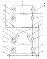
- a first embodiment of a switching cell according to the invention is shown.
- the switching cell has a switching group 1, wherein the switching group 1, a first and a second controllable bidirectional power semiconductor switch 2, 3 and a capacitor 25.
- the switching group 1 further comprises a third, fourth, fifth and sixth controllable bidirectional power semiconductor switch 4, 5, 6, 7, wherein the first controllable bidirectional power semiconductor switch 2 is antiserially connected to the second controllable bidirectional power semiconductor switch 3 and the third controllable bidirectional power semiconductor switch antiserial to the fourth controllable bidirectional power semiconductor switch 5 is connected.
- the capacitor 25 of the switching group is further connected to the connection point of the first drivable bidirectional power semiconductor switch 2 to the second drivable bidirectional power semiconductor switch 3 and the connection point of the third drivable bidirectional power semiconductor switch 4 to the fourth drivable bidirectional power semiconductor switch 5.
- the fifth controllable bidirectional power semiconductor switch 6 is also connected to the connection point of the first controllable bidirectional power semiconductor switch 2 to the second controllable bidirectional power semiconductor switch 3 and the fourth controllable bidirectional power semiconductor switch 5, wherein the sixth controllable bidirectional power semiconductor switch 7 with the connection point of the third controllable bidirectional power semiconductor switch is connected to the fourth controllable bidirectional power semiconductor switch 5 and to the second controllable bidirectional power semiconductor switch 3.
- a first and a first series-connected second capacitive energy storage 8, 9 are provided, wherein the first controllable bidirectional power semiconductor switch 2 and the third controllable bidirectional power semiconductor switch 4 connected at the connection point of the first capacitive energy storage device 8 with the second capacitive energy storage 9 are.
- the stored electrical energy of the switching cell can be advantageously kept low, the dielectric strength or the Blocking voltage of the individual controllable bidirectional power semiconductor switches 2, 3, 4, 5, 6, 7 only the voltage of the capacitor 25, the maximum applied to the capacitor 25 must correspond, and the individual controllable bidirectional power semiconductor switches 2, 3, 4, 5, 6, 7 Therefore, with regard to their blocking voltage, they merely have to be designed for this voltage.
- n further switching groups 1.1, ... 1.n are provided, which each have a first, second, third and fourth controllable bidirectional power semiconductor switch 20, 21, 22, 23 and a capacitor 24 .
- the capacitor 24 is connected to the first drivable bidirectional power semiconductor switch 20 and to the second drivable bidirectional power semiconductor switch 21, the third controllable bidirectional power semiconductor switch 22 to the connection point of the capacitor 24 to the first drivable bidirectional power semiconductor switch 20 and connected to the second drivable bidirectional power semiconductor switch 21.
- the fourth controllable bidirectional power semiconductor switch 23 is connected to the connection point of the capacitor 24 to the second drivable bidirectional power semiconductor switch 21 and to the first drivable bidirectional power semiconductor switch 20. Since it is according to Fig. 2 each of the n further switching groups 1.1, ... 1.n is a quadrupole, each of the n further switching groups 1.1,... 1.n is linked to the respectively adjacent further switching group 1.1,. wherein the switching group 1 is connected to the first further switching group 1.1.
- connection point of the sixth controllable bidirectional power semiconductor switch 7 with the second controllable bidirectional power semiconductor switch 3 of Switching group 1 is connected to the connection point of the capacitor 24 to the first controllable bidirectional power semiconductor switch 20 of the first further switching group 1.1.
- connection point of the fifth controllable bidirectional power semiconductor switch 6 to the fourth controllable bidirectional power semiconductor switch 5 of the switching group 1 is connected to the connection point of the capacitor 24 to the second controllable bidirectional power semiconductor switch 21 of the first further switching group 1.1.
- the first, second, third, fourth, fifth and sixth controllable bidirectional power semiconductor switches 2, 3, 4, 5, 6, 7 of the switching group 1 preferably each have at least two controllable bidirectional switching elements, wherein the controllable bidirectional switching elements are connected in series.
- the voltage to be switched on the respective controllable bidirectional power semiconductor switch 2, 3, 4, 5, 6, 7 can thus be increased.
- the first, second, third and fourth controllable bidirectional power semiconductor switches 20, 21, 22, 23 of each n further switching group 1.1, ... 1.n each have at least two controllable bidirectional switching elements, in which case the controllable bidirectional switching elements in Series are switched. Even then, the voltage to be switched on the respective controllable bidirectional power semiconductor switches 20, 21, 22, 23 can advantageously be increased. Accordingly, an arbitrary number of controllable bidirectional switching elements for each controllable bidirectional power semiconductor switch 2, 3, 4, 5, 6, 7, 20, 21, 22, 23 of the switch cell 1 with respect to the embodiments according to Fig. 1 and Fig. 2 conceivable.
- a first embodiment of an inventive converter circuit is shown, the inventive a switching cell 1 according to Fig. 1 having. Furthermore, in the inverter circuit after Fig. 3 a phase switching cell 10 is provided, wherein the phase switching cell 10 has a first, second, third, fourth, fifth and sixth controllable bidirectional power semiconductor switch 11, 12, 13, 14, 15, 16 and the first controllable bidirectional power semiconductor switch 11 of the phase switching cell 10 in series with the second controllable bidirectional power semiconductor switch 12 of the phase switching cell 10, the third controllable bi-directional power semiconductor switch 13 of the phase switch cell 10 is connected in series with the fourth controllable bidirectional power semiconductor switch 14 of the phase switch cell 10 and the fifth controllable bidirectional power semiconductor switch 15 of the phase switch cell 10 with the connection point of the first controllable bidirectional power semiconductor switch 11 with the second controllable bidirectional Power semiconductor switch 12 of the phase switching cell 10 is connected.
- the sixth controllable bidirectional power semiconductor switch 16 of the phase switch cell 10 is further connected to the connection point of the third controllable bidirectional power semiconductor switch 13 to the fourth controllable bidirectional power semiconductor switch 14 of the phase switch cell 10. Furthermore, the first controllable bidirectional power semiconductor switch 11 of the phase switching cell 10 according to Fig. 3 connected to the first capacitive energy storage 8 of the switching cell 1, wherein the second controllable bidirectional power semiconductor switch 12 of the phase switching cell 10 is connected to the connection point of the sixth controllable bidirectional power semiconductor switch 7 to the second controllable bidirectional power semiconductor switch 3 of the switching cell 1.
- the fourth controllable bidirectional power semiconductor switch 14 of the phase switching cell 10 is connected to the second capacitive energy storage 9 of the switching cell 1, wherein the third controllable bidirectional power semiconductor switch 13 of the phase switching cell 10 with the connection point of the fifth controllable bidirectional power semiconductor switch 6 with the fourth controllable bidirectional power semiconductor switch 5 of the switching cell 1 is connected.
- a phase-switching cell 10 is provided, the phase-switching cell 10 having a first, second, third, fourth, fifth and sixth controllable bidirectional power semiconductor switches 11, 12, 13, 14, 15, 16 and the first controllable bidirectional power semiconductor switch 11 of the phase switching cell 10 serially is connected to the second controllable bidirectional power semiconductor switch 12 of the phase switching cell 10, the third controllable bidirectional power semiconductor switch 13 of the phase switching cell 10 is connected in series with the fourth controllable bidirectional power semiconductor switch 14 of the phase switching cell 10 and the fifth controllable bidirectional power semiconductor switch 15 of the phase switching cell 10 is connected to the connection point of the first with the second controllable bidirectional power semiconductor switch 11, 12 of the phase switching cell 10.
- the sixth controllable bidirectional power semiconductor switch 16 of the phase switching cell 10 is also connected to the connection point of the third controllable bidirectional power semiconductor switch 13, 14 of the phase switch cell 10, the first controllable bidirectional power semiconductor switch 11 of the phase switch cell 10 connected to the first capacitive energy storage 8 of the switch cell 1 and the second controllable bidirectional power semiconductor switch 12 of the phase switch cell 10 is connected to the connection point of the fourth controllable bidirectional power semiconductor switch 23 to the first controllable bidirectional power semiconductor switch 20 of the nth further switch cell 1.n.
- the fourth controllable bidirectional power semiconductor switch 14 of the phase switching cell 10 is connected to the second capacitive energy store 9 of the switching cell 1, wherein the third controllable bidirectional power semiconductor switch 13 of the phase switching cell 10 with the connection point of the third controllable bidirectional power semiconductor switch 22 with the second controllable bidirectional power semiconductor switch 21 of n-th further switching cell 1.n is connected. Accordingly, a multiplicity of switching voltage levels are possible by means of the converter circuit described above, which depends in particular on the number n of further switching groups 1.1,... 1.n.
- the stored electrical energy of the realized converter circuit are advantageously kept low. Due to the low stored electrical energy of the converter circuit as a whole, the converter circuit can be kept small and thus takes up very little space. For many applications, for example for tractor applications, the converter circuit is thus predestined. Furthermore, the converter circuit by the switching cell 1 and phase switching cell 10 comes with a smaller number of components compared to conventional converter circuits to achieve the switching voltage levels. In addition, the converter circuit through the switching cell 1 and phase switching cell 10 is very voltage resistant and thus insensitive to high voltages and fault conditions and has low overall active power losses.
- the fifth and sixth controllable bidirectional power semiconductor switches 15, 16 of the phase-switching cell 10 are preferably connected to one another and accordingly form a phase connection, in particular for the phase R as in FIG Fig. 3 shown by way of example.
- the phase-switching cell 10 has a seventh and an eighth controllable bidirectional power semiconductor switch 17, 18 and a capacitor 19, the capacitor 19 of the phase-switching cell 10 being connected to the fifth and sixth controllable bidirectional power semiconductor switches 15, 16 of the phase-switching cell 10. Furthermore, the seventh controllable bidirectional power semiconductor switch 17 of the phase switching cell 10 is according to Fig.
- Fig. 4 and Fig. 5 is preferably formed by a bipolar transistor with insulated drive electrode (IGBT - Insulated Gate Bipolartransistor) and by a diode connected in anti-parallel.
- the respective controllable Bidirectional power semiconductor switch 11, 12, 13, 14 of the phase-switching cell 10 is also formed by a bipolar transistor with insulated drive electrode arranged (IGBT - Insulated Gate Bipolartransistor) and by a diode connected in parallel thereto.
- the first, second, third and fourth controllable bidirectional power semiconductor switches 11, 12, 13, 14 of the phase-switching cell 10 preferably each have at least two controllable bidirectional switching elements, wherein the controllable bidirectional switching elements are connected in series.
- the voltage to be switched on the respective controllable bidirectional power semiconductor switch 11, 12, 13, 14 of the phase-switching cell 10 can thus be increased.
- the respective switching element can be formed by a bipolar transistor with insulated drive electrode (IGBT) and by a diode connected in antiparallel or by an integrated thyristor with commutated drive electrode (IGCT) and by a diode connected in antiparallel thereto ,
- Fig. 5 a third embodiment of the inventive converter circuit shown.
- the converter circuit after Fig. 5 is advantageously suitable for connection to a plurality of phases R, S, T, wherein the converter circuit according to Fig. 5 only as an example only for connection to three phases R, S, T is shown, but in general any number of phases can be connected.
- a phase-switching cell 10 is provided for each phase R, S, T, as in FIG Fig. 5 exemplified.
- the first controllable bidirectional power semiconductor switch 11 1 of each phase switching cell 10 is connected to the first capacitive energy storage 8 of the switching cell 1, wherein the second controllable bidirectional power semiconductor switch 12 of each phase switching cell 10 with the connection point of the sixth controllable bidirectional power semiconductor switch 7 with the second controllable bidirectional power semiconductor switch 3 of the switching cell 1 is connected.
- the fourth controllable bidirectional power semiconductor switch 14 of each phase switching cell 10 is also connected to the second capacitive energy storage 9 of the switching cell 1, wherein the third controllable bidirectional power semiconductor switch 13 of each phase switching cell 10 with the connection point of the fifth controllable bidirectional power semiconductor switch 6 with the fourth controllable bidirectional power semiconductor switch 5 of the switching cell 1 is connected.
- a phase-switching cell 10 is initially provided again for each phase R, S, T.
- the first controllable bidirectional power semiconductor switch 11 of each phase switching cell 10 is connected to the first capacitive energy storage 8 of the switching cell 1, wherein the second controllable bidirectional power semiconductor switch 12 of each phase switching cell 10 with the connection point of the fourth controllable bidirectional power semiconductor switch 23 with the first controllable bidirectional power semiconductor switch 20 of the nth further switching cell 1.n is connected.
- the fourth controllable bidirectional power semiconductor switch 14 of each phase switching cell 10 is connected to the second capacitive energy store 9 of the switching cell 1, the third controllable bidirectional power semiconductor switch 13 of each phase switching cell 10 with the connection point of the third controllable bidirectional power semiconductor switch 22 with the second controllable bidirectional power semiconductor switch 21st the nth further switching cell 1.n is connected.
Abstract
Description
Die Erfindung bezieht sich auf das Gebiet der Umrichterschaltungen. Sie geht aus von einer Schaltzelle für eine Umrichterschaltung zur Schaltung einer Vielzahl von Spannungsniveaus gemäss dem Oberbegriff des unabhängigen Anspruchs 1.The invention relates to the field of converter circuits. It is based on a switching cell for a converter circuit for switching a plurality of voltage levels according to the preamble of the
Umrichterschaltungen werden heute in einer Fülle von leistungselektronischen Anwendungen eingesetzt. Die Anforderungen an eine solche Umrichterschaltung sind dabei zum einen, möglichst wenig Oberschwingungen an Phasen eines an die Umrichterschaltung gängigerweise angeschlossenen elektrischen Wechselspannungsnetzes zu erzeugen und zum anderen mit einer möglichst geringen Anzahl an elektronischen Bauelementen möglichst grosse Leistungen zu übertragen. Eine geeignete Umrichterschaltung zur Schaltung einer Vielzahl von Schaltspannungsniveaus ist in der
In "
Problematisch bei einer Schaltzelle der Umrichterschaltung zur Schaltung einer Vielzahl von Schaltspannungsniveaus nach der
Aufgabe der Erfindung ist es deshalb, eine Schaltzelle anzugeben, die möglichst wenig elektrische Energie während ihres Betriebes speichert und platzsparend realisiert werden kann. Weiterhin ist es eine Aufgabe der Erfindung, eine Umrichterschaltung zur Schaltung einer Vielzahl von Spannungsniveaus anzugeben, die ebenfalls möglichst wenig elektrische Energie während ihres Betriebes speichert, platzsparend realisiert werden kann, weitestgehend unempfindlich gegen hohe Spannungen und Fehlerzustände ist und geringe Wirkleistungsverluste aufweist. Diese Aufgaben werden durch die Merkmale des Anspruchs 1 und des Anspruchs 6 gelöst. In den abhängigen Ansprüchen sind vorteilhafte Weiterbildungen der Erfindung angegeben.The object of the invention is therefore to provide a switching cell that saves as little electrical energy during their operation and can be realized to save space. Furthermore, it is an object of the invention to provide a converter circuit for switching a variety of voltage levels, which also saves as little electrical energy during their operation, can be realized to save space, is largely insensitive to high voltages and fault conditions and has low active power losses. These objects are achieved by the features of
Die erfindungsgemässe Schaltzelle umfasst eine Schaltgruppe, wobei die Schaltgruppe einen ersten und einen zweiten ansteuerbaren bidirektionalen Leistungshalbleiterschalter und einen Kondensator aufweist. Nach der Erfindung weist die Schaltgruppe zudem einen dritten, vierten, fünften und sechsten ansteuerbaren bidirektionalen Leistungshalbleiterschalter auf, wobei der erste ansteuerbare bidirektionale Leistungshalbleiterschalter antiseriell zu dem zweiten ansteuerbaren bidirektionalen Leistungshalbleiterschalter geschaltet ist und der dritte ansteuerbare bidirektionale Leistungshalbleiterschalter antiseriell zu dem vierten ansteuerbaren bidirektionalen Leistungshalbleiterschalter geschaltet ist. Der Kondensator ist weiterhin mit dem Verbindungspunkt des ersten ansteuerbaren bidirektionalen Leistungshalbleiterschalters mit dem zweiten ansteuerbaren bidirektionalen Leistungshalbleiterschalter und mit dem Verbindungspunkt des dritten ansteuerbaren bidirektionalen Leistungshalbleiterschalters mit dem vierten ansteuerbaren bidirektionalen Leistungshalbleiterschalter verbunden. Der fünfte ansteuerbare bidirektionale Leistungshalbleiterschalter ist zudem mit dem Verbindungspunkt des ersten ansteuerbaren bidirektionalen Leistungshalbleiterschalters mit dem zweiten ansteuerbaren bidirektionalen Leistungshalbleiterschalter und mit dem vierten ansteuerbaren bidirektionalen Leistungshalbleiterschalter verbunden, wobei der sechste ansteuerbare bidirektionale Leistungshalbleiterschalter mit dem Verbindungspunkt des dritten ansteuerbaren bidirektionalen Leistungshalbleiterschalters mit dem vierten ansteuerbaren bidirektionalen Leistungshalbleiterschalter und mit dem zweiten ansteuerbaren bidirektionalen Leistungshalbleiterschalter verbunden ist. Darüber hinaus sind ein erster und ein zu dem ersten in Serie geschalteter zweiter kapazitiver Energiespeicher vorgesehen, wobei der erste ansteuerbare bidirektionale Leistungshalbleiterschalter und der dritte ansteuerbare bidirektionale Leistungshalbleiterschalter am Verbindungspunkt des ersten kapazitiven Energiespeichers mit dem zweiten kapazitiven Energiespeicher miteinander verbunden sind. Mittels der ansteuerbaren bidirektionalen Leistungshalbleiterschalter, des Kondensators, der beiden kapazitiven Energiespeicher und deren vorstehend beschriebenen Verbindungen zueinander und untereinander, kann die gespeicherte elektrische Energie der Schaltzelle vorteilhaft gering gehalten werden, wobei die Spannungsfestigkeit bzw. die Blockierspannung der einzelnen ansteuerbaren bidirektionalen Leistungshalbleiterschalter mit Vorteil nur der Spannung des Kondensators, die maximal am Kondensator anliegt, entsprechen muss und die einzelnen ansteuerbaren bidirektionalen Leistungshalbleiterschalter bezüglich ihre Blockierspannung demnach lediglich auf diese Spannung ausgelegt sein müssen. Aufgrund der geringen gespeicherten elektrischen Energie der Schaltzelle insgesamt, kann diese klein gehalten werden, da der Kondensator der Schaltzelle nur für diese kleine zu speichernde elektrische Energie, d.h. bezüglich ihrer Spannungsfestigkeit und/oder ihrer Kapazität, ausgelegt werden muss. Aufgrund der daraus resultierenden geringen Baugrösse des Kondensators benötigt die Schaltzelle sehr wenig Platz. Ferner kann durch die geringe Baugrösse auch der Montage- und Wartungsaufwand gering gehalten werden.The inventive switching cell comprises a switching group, wherein the switching group has a first and a second controllable bidirectional power semiconductor switch and a capacitor. According to the invention, the switching group further comprises a third, fourth, fifth and sixth controllable bidirectional power semiconductor switch, wherein the first controllable bidirectional power semiconductor switch is antiserially connected to the second controllable bidirectional power semiconductor switch and the third controllable bidirectional power semiconductor switch is connected antiserially to the fourth controllable bidirectional power semiconductor switch , The capacitor is further connected to the junction of the first drivable bidirectional power semiconductor switch with the second drivable bidirectional power semiconductor switch and to the connection point of the third drivable bidirectional power semiconductor switch with the fourth drivable bidirectional power semiconductor switch. The fifth addressable bidirectional power semiconductor switch is also connected to the connection point of the first bidirectional power semiconductor switch to the second bidirectional power semiconductor switch and to the fourth bidirectional power semiconductor switch, the sixth addressable bidirectional power semiconductor switch to the connection point of the third bidirectional power semiconductor switch to the fourth bidirectional power semiconductor switch and connected to the second drivable bidirectional power semiconductor switch. In addition, a first and a second capacitive energy store connected in series with the first are provided, the first controllable bidirectional power semiconductor switch and the third controllable bidirectional power semiconductor switch being connected to one another at the connection point of the first capacitive energy store with the second capacitive energy store. By means of the controllable bidirectional power semiconductor switch, the capacitor, the two capacitive energy storage and their above-described connections to each other and each other, the stored electrical energy of the switching cell can be kept advantageously low, the dielectric strength or the blocking voltage of the individual controllable bidirectional power semiconductor switch with advantage only the Voltage of the capacitor, which is applied to the maximum capacitor, must correspond and the individual controllable Therefore, bidirectional power semiconductor switch with respect to their blocking voltage must be designed only to this voltage. Due to the low stored electrical energy of the switching cell as a whole, this can be kept small because the capacitor of the switching cell only for this small electrical energy to be stored, ie with respect to their dielectric strength and / or their capacity must be designed. Due to the resulting small size of the capacitor, the switching cell requires very little space. Furthermore, the installation and maintenance costs can be kept low due to the small size.
Die erfindungsgemässe Umrichterschaltung zur Schaltung einer Vielzahl von Spannungsniveaus umfasst die erfindungsgemässe Schaltzelle und zusätzlich eine Phasenschaltzelle, wobei die Phasenschaltzelle einen ersten, zweiten, dritten, vierten, fünften und sechsten ansteuerbaren bidirektionalen Leistungshalbleiterschalter aufweist und der erste ansteuerbare bidirektionale Leistungshalbleiterschalter der Phasenschaltzelle seriell zu dem zweiten ansteuerbaren bidirektionalen Leistungshalbleiterschalter der Phasenschaltzelle geschaltet ist, der dritte ansteuerbare bidirektionale Leistungshalbleiterschalter der Phasenschaltzelle seriell zu dem vierten ansteuerbaren bidirektionalen Leistungshalbleiterschalter der Phasenschaltzelle geschaltet ist und der fünfte ansteuerbare bidirektionale Leistungshalbleiterschalter der Phasenschaltzelle mit dem Verbindungspunkt des ersten ansteuerbaren bidirektionalen Leistungshalbleiterschalter mit dem zweiten ansteuerbaren bidirektionalen Leistungshalbleiterschalter der Phasenschaltzelle verbunden ist. Der sechste ansteuerbare bidirektionale Leistungshalbleiterschalter der Phasenschaltzelle ist ferner mit dem Verbindungspunkt des dritten ansteuerbaren bidirektionalen Leistungshalbleiterschalters mit dem vierten ansteuerbaren bidirektionalen Leistungshalbleiterschalter der Phasenschaltzelle verbunden. Zudem ist der erste ansteuerbare bidirektionale Leistungshalbleiterschalter der Phasenschaltzelle mit dem ersten kapazitiven Energiespeichers der Schaltzelle verbunden, wobei der zweite ansteuerbare bidirektionale Leistungshalbleiterschalter der Phasenschaltzelle mit dem Verbindungspunkt des sechsten ansteuerbaren bidirektionalen Leistungshalbleiterschalter mit dem zweiten ansteuerbaren bidirektionalen Leistungshalbleiterschalter der Schaltzelle verbunden ist. Der vierte ansteuerbare bidirektionale Leistungshalbleiterschalter der Phasenschaltzelle ist weiterhin mit dem zweiten kapazitiven Energiespeichers der Schaltzelle verbunden, wobei der dritte ansteuerbare bidirektionale Leistungshalbleiterschalter der Phasenschaltzelle mit dem Verbindungspunkt des fünften ansteuerbaren bidirektionalen Leistungshalbleiterschalter mit dem vierten ansteuerbaren bidirektionalen Leistungshalbleiterschalter der Schaltzelle verbunden ist. Mittels der ansteuerbaren bidirektionalen Leistungshalbleiterschalter der Phasenschaltzelle und der erfindungsgemässen Schaltzelle kann die gespeicherte elektrische Energie der damit realisierten Umrichterschaltung vorteilhaft gering gehalten werden. Aufgrund der geringen gespeicherten elektrischen Energie der Umrichterschaltung insgesamt, kann die Umrichterschaltung klein gehalten werden und beansprucht somit sehr wenig Platz. Für viele Anwendungen, beispielsweise für Traktionsanwendungen, ist die Umrichterschaltung damit prädestiniert. Desweiteren kommt die Umrichterschaltung durch die Schaltzelle und Phasenschaltzelle mit einer geringeren Anzahl an Bauelementen im Vergleich zu gängigen Umrichterschaltungen zur Erreichung der Schaltspannungsniveaus aus. Darüberhinaus ist die Umrichterschaltung durch die Schaltzelle und Phasenschaltzelle sehr spannungsfest und damit unempfindlich gegen hohe Spannungen und Fehlerzustände und weist insgesamt geringe Wirkleistungsverluste auf.The inventive converter circuit for switching a plurality of voltage levels comprises the switching cell according to the invention and additionally a phase switching cell, wherein the phase switching cell has a first, second, third, fourth, fifth and sixth controllable bidirectional power semiconductor switch and the first controllable bidirectional power semiconductor switch of the phase switching cell serially to the second controllable The third controllable bidirectional power semiconductor switch of the phase switching cell is connected in series with the fourth controllable bidirectional power semiconductor switch of the phase switching cell and the fifth controllable bidirectional power semiconductor switch of the phase switching cell with the connection point of the first controllable bidirectional power semiconductor switch with the second controllable bidirectional Leistungshalble iterschalter the phase switching cell is connected. The sixth controllable bidirectional power semiconductor switch of the phase-switching cell is further connected to the connection point of the third controllable bidirectional power semiconductor switch with the fourth controllable bidirectional power semiconductor switch of the phase-switching cell. In addition, the first controllable bidirectional power semiconductor switch of the phase switching cell is connected to the first capacitive energy storage of the switching cell, wherein the second controllable bidirectional power semiconductor switch of the phase switching cell is connected to the connection point of the sixth controllable bidirectional power semiconductor switch to the second controllable bidirectional power semiconductor switch of the switching cell. The fourth controllable bidirectional power semiconductor switch of the phase switching cell is further connected to the second capacitive energy storage of the switching cell, wherein the third controllable bidirectional power semiconductor switch of the phase switching cell with the connection point of the fifth controllable bidirectional power semiconductor switch with the fourth controllable bidirectional power semiconductor switch of the switching cell connected is. By means of the controllable bidirectional power semiconductor switches of the phase-switching cell and the inventive switching cell, the stored electrical energy of the converter circuit realized thereby can advantageously be kept low. Due to the low stored electrical energy of the converter circuit as a whole, the converter circuit can be kept small and thus takes up very little space. For many applications, for example for traction applications, the converter circuit is thus predestined. Furthermore, the converter circuit comes through the switching cell and phase switching cell with a smaller number of components compared to conventional converter circuits to achieve the switching voltage levels. Moreover, the converter circuit through the switching cell and phase switching cell is very voltage resistant and thus insensitive to high voltages and fault conditions and has low overall active power losses.
Diese und weitere Aufgaben, Vorteile und Merkmale der vorliegenden Erfindung werden aus der nachfolgenden detaillierten Beschreibung bevorzugter Ausführungsformen der Erfindung in Verbindung mit der Zeichnung offensichtlich.These and other objects, advantages and features of the present invention will become more apparent from the following detailed description of preferred embodiments of the invention taken in conjunction with the accompanying drawings.
Es zeigen:
- Fig. 1
- eine erste Ausführungsform einer erfindungsgemässen Schaltzelle,
- Fig. 2
- eine zweite Ausführungsform der erfindungsgemässen Schaltzelle,
- Fig. 3
- eine erste Ausführungsform einer efindungsgemässen Umrichterschaltung,
- Fig. 4
- eine zweite Ausführungsform der erfindungsgemässen Umrichterschaltung und
- Fig. 5
- eine dritte Ausführungsform der erfindungsgemässen Umrichterschaltung.
- Fig. 1
- a first embodiment of a switching cell according to the invention,
- Fig. 2
- a second embodiment of the inventive switching cell,
- Fig. 3
- A first embodiment of a converter circuit according to the invention,
- Fig. 4
- a second embodiment of the inventive converter circuit and
- Fig. 5
- A third embodiment of the inventive converter circuit.
Die in der Zeichnung verwendeten Bezugszeichen und deren Bedeutung sind in der Bezugszeichenliste zusammengefasst aufgelistet. Grundsätzlich sind in den Figuren gleiche Teile mit gleichen Bezugszeichen versehen. Die beschriebenen Ausführungsformen stehen beispielhaft für den Erfindungsgegenstand und haben keine beschränkende Wirkung.The reference numerals used in the drawings and their meaning are listed in the list of reference numerals. Basically, the same parts are provided with the same reference numerals in the figures. The described embodiments are exemplary of the subject invention and have no limiting effect.
In
In
Der erste, zweite, dritte, vierte, fünfte und sechste ansteuerbare bidirektionale Leistungshalbleiterschalter 2, 3, 4, 5, 6, 7 der Schaltgruppe 1 weist vorzugsweise jeweils mindestens zwei ansteuerbare bidirektionale Schaltelemente auf, wobei die ansteuerbaren bidirektionalen Schaltelemente in Serie geschaltet sind. Vorteilhaft lässt sich damit die zu schaltende Spannung an dem jeweiligen ansteuerbaren bidirektionalen Leistungshalbleiterschalter 2, 3, 4, 5, 6, 7 erhöhen. Darüber hinaus kann auch der erste, zweite, dritte und vierte ansteuerbare bidirektionale Leistungshalbleiterschalter 20, 21, 22, 23 einer jeden n weiteren Schaltgruppe 1.1, ... 1.n jeweils mindestens zwei ansteuerbare bidirektionale Schaltelemente aufweisen, wobei dann die ansteuerbaren bidirektionalen Schaltelemente in Serie geschaltet sind. Auch dann lässt sich die zu schaltende Spannung an dem jeweiligen ansteuerbaren bidirektionalen Leistungshalbleiterschalter 20, 21, 22, 23 mit Vorteil erhöhen. Demnach ist eine beliebige Anzahl an ansteuerbaren bidirektionalen Schaltelementen für jeden ansteuerbaren bidirektionalen Leistungshalbleiterschalter 2, 3, 4, 5, 6, 7, 20, 21, 22, 23 der Schaltzelle 1 bezüglich der Ausführungsformen nach
In
In einer nicht dargestellten alternativen Variante der vorstehend beschriebenen ersten Ausführungsform der erfindungsgemässen Umrichterschaltung nach
Mittels der ansteuerbaren bidirektionalen Leistungshalbleiterschalter 11, 12, 13, 14, 15, 16 der Phasenschaltzelle 10 und der ansteuerbaren bidirektionalen Leistungshalbleiterschalter 2, 3, 4, 5, 6, 7, 20, 21, 22, 23 der erfindungsgemässen Schaltzelle 1 kann die gespeicherte elektrische Energie der damit realisierten Umrichterschaltung vorteilhaft gering gehalten werden. Aufgrund der geringen gespeicherten elektrischen Energie der Umrichterschaltung insgesamt, kann die Umrichterschaltung klein gehalten werden und beansprucht somit sehr wenig Platz. Für viele Anwendungen, beispielsweise für Traktiönsanwendungen, ist die Umrichterschaltung damit prädestiniert. Desweiteren kommt die Umrichterschaltung durch die Schaltzelle 1 und Phasenschaltzelle 10 mit einer geringeren Anzahl an Bauelementen im Vergleich zu gängigen Umrichterschaltungen zur Erreichung der Schaltspannungsniveaus aus. Darüberhinaus ist die Umrichterschaltung durch die Schaltzelle 1 und Phasenschaltzelle 10 sehr spannungsfest und damit unempfindlich gegen hohe Spannungen und Fehlerzustände und weist insgesamt geringe Wirkleistungsverluste auf.By means of the controllable bidirectional power semiconductor switches 11, 12, 13, 14, 15, 16 of the
Vorzugsweise sind der fünfte und sechste ansteuerbare bidirektionale Leistungshalbleiterschalter 15, 16 der Phasenschaltzelle 10 miteinander verbunden und bilden demnach einen Phasenanschluss, insbesondere für die Phase R wie in
In Weiterentwicklung der Umrichterschaltung nach
Der jeweilige ansteuerbare bidirektionale Leistungshalbleiterschalter 2, 3, 4, 5, 6, 7, 20, 21, 22, 23 der Schaltzelle 1 nach
In Weiterentwicklung der Umrichterschaltung nach
In Weiterentwicklung der vorstehend im Detail beschriebenen nicht dargestellten Umrichterschaltung ist es denkbar, dass zum Anschluss an mehrere, d.h. allgemein an beliebig viele Phasen R, S, T zunächst wieder für jede Phase R, S, T eine Phasenschaltzelle 10 vorgesehen ist. Im Unterschied zur Ausführungsform der Umrichterschaltung nach
- 11
- Schaltgruppeswitching group
- 1.1,... 1.n1.1, ... 1.n
- n weitere Schaltgruppenn further switching groups
- 22
- erster ansteuerbarer bidirektionaler Leistungshalbleiterschalter der Schalt- gruppefirst controllable bidirectional power semiconductor switch of the switching group
- 33
- zweiter ansteuerbarer bidirektionaler Leistungshalbleiterschalter der Schalt- gruppesecond controllable bidirectional power semiconductor switch of the switching group
- 44
- dritter ansteuerbarer bidirektionaler Leistungshalbleiterschalter der Schalt- gruppethird controllable bidirectional power semiconductor switch of the switching group
- 55
- vierter ansteuerbarer bidirektionaler Leistungshalbleiterschalter der Schalt- gruppefourth controllable bidirectional power semiconductor switch of the switching group
- 66
- fünfter ansteuerbarer bidirektionaler Leistungshalbleiterschalter der Schalt- gruppefifth controllable bidirectional power semiconductor switch of the switching group
- 77
- sechster ansteuerbarer bidirektionaler Leistungshalbleiterschalter der Schalt- gruppesixth controllable bidirectional power semiconductor switch of the switching group
- 88th
- erster kapazitiver Energiespeicherfirst capacitive energy storage
- 99
- zweiter kapazitiver Energiespeichersecond capacitive energy storage
- 1010
- PhasenschaltzellePhase switching cell
- 1111
- erster ansteuerbarer bidirektionaler Leistungshalbleiterschalter der Phasen- schaltzellefirst controllable bidirectional power semiconductor switch of the phase switching cell
- 1212
- zweiter ansteuerbarer bidirektionaler Leistungshalbleiterschalter der Phasen- schaltzellesecond controllable bidirectional power semiconductor switch of the phase switching cell
- 1313
- dritter ansteuerbarer bidirektionaler Leistungshalbleiterschalter der Phasen- schaltzellethird controllable bidirectional power semiconductor switch of the phase switching cell
- 1414
- vierter ansteuerbarer bidirektionaler Leistungshalbleiterschalter der Phasen- schaltzellefourth controllable bidirectional power semiconductor switch of the phase switching cell
- 1515
- fünfter ansteuerbarer bidirektionaler Leistungshalbleiterschalter der Phasen- schaltzellefifth controllable bidirectional power semiconductor switch of the phase switching cell
- 1616
- sechster ansteuerbarer bidirektionaler Leistungshalbleiterschalter der Phasen- schaltzellesixth controllable bidirectional power semiconductor switch of the phase switching cell
- 1717
- siebter ansteuerbarer bidirektionaler Leistungshalbleiterschalter der Phasen- schaltzelleseventh controllable bidirectional power semiconductor switch of the phase switching cell
- 1818
- achter ansteuerbarer bidirektionaler Leistungshalbleiterschalter der Phasen- schaltzelleeighth controllable bidirectional power semiconductor switch of the phase switching cell
- 1919
- Kondensator der PhasenschaltzelleCapacitor of the phase switching cell
- 2020
- erster ansteuerbarer bidirektionaler Leistungshalbleiterschalter der n weiteren Schaltgruppenfirst controllable bidirectional power semiconductor switch of the n other switching groups
- 2121
- zweiter ansteuerbarer bidirektionaler Leistungshalbleiterschalter der n weiteren Schaltgruppensecond controllable bidirectional power semiconductor switch of the n other switching groups
- 2222
- dritter ansteuerbarer bidirektionaler Leistungshalbleiterschalter der n weiteren Schaltgruppenthird controllable bidirectional power semiconductor switch of the n other switching groups
- 2323
- vierter ansteuerbarer bidirektionaler Leistungshalbleiterschalter der n weiteren Schaltgruppenfourth controllable bidirectional power semiconductor switch of the n further switching groups
- 2424
- Kondensator der n weiteren SchaltgruppenCapacitor of n other switching groups
- 2525
- Kondensator der SchaltgruppeCapacitor of the switching group
Claims (12)
- Switchgear cell for a converter circuit for switching a multiplicity of voltage levels having a group of connection (1), with the group of connection (1) having a first and a second controllable bidirectional power semiconductor switch (2, 3) and a capacitor (25),
characterized
in that the group of connection (1) has a third, fourth, fifth and sixth controllable bidirectional power semiconductor switch (4, 5, 6, 7) and the first controllable bidirectional power semiconductor switch (2) is connected back-to-back in series with the second controllable bidirectional power semiconductor switch (3), the third controllable bidirectional power semiconductor switch (4) is connected back-to-back in series with the fourth controllable bidirectional power switch (5), the capacitor (25) is connected to the connection point of the first controllable bidirectional power semiconductor switch (2) to the second controllable bidirectional power semiconductor switch (3) and to the connection point of the third controllable bidirectional power semiconductor switch (4) to the fourth controllable bidirectional power semiconductor switch (5), the fifth controllable bidirectional power semiconductor switch (6) is connected to the connection point of the first controllable bidirectional power semiconductor switch (2) to the second controllable bidirectional power semiconductor switch (3), and to the fourth controllable bidirectional power semiconductor switch (5), and the sixth controllable bidirectional power semiconductor switch (7) is connected to the connection point of the third controllable bidirectional power semiconductor switch (4) to the fourth controllable bidirectional power semiconductor switch (5) and to the second controllable bidirectional power semiconductor switch (3),
in that a first and a second, which is connected in series with the first, capacitive energy store (8, 9) are provided, and
in that the first controllable bidirectional power semiconductor switch (2) and the third controllable bidirectional power semiconductor switch (4) are connected to one another at the connection point of the first capacitive energy store (8) to the second capacitive energy store (9). - Switchgear cell according to Claim 1, characterized in that further groups of connection (1.1, ... 1.n) are provided and each have a first, second, third, and fourth controllable bidirectional power semiconductor switch (20, 21, 22, 23) and a capacitor (24) where n ≥ 1, and the capacitor (24) in each of the n further groups of connection (1.1, ... 1.n) is connected to the first controllable bidirectional power semiconductor switch (20) and to the second controllable bidirectional power semiconductor switch (21), the third controllable bidirectional power semiconductor switch (22) is connected to the connection point of the capacitor (24), to the first controllable bidirectional power semiconductor switch (20) and to the second controllable bidirectional power semiconductor switch (21), and the fourth controllable bidirectional power semiconductor switch (23) is connected to the connection point of the capacitor (24), to the second controllable bidirectional
power semiconductor switch (21) and to the first controllable bidirectional power semiconductor switch (20),
in that each of the n further groups of connection (1.1, ...1.n) is connected in a linked form to the respectively adjacent further group of connection (1.1, ...1.n), and
in that the group of connection (1) is connected to the first further group of connection (1.1). - Switchgear cell according to Claim 2, characterized in that the connection point of the sixth controllable bidirectional power semiconductor switch (7) to the second controllable bidirectional power semiconductor switch (3) in the group of connection (1) is connected to the connection point of the capacitor (24) to the first controllable bidirectional power semiconductor switch (20) in the first further group of connection (1.1), and
in that the connection point of the fifth controllable bidirectional power semiconductor switch (6) to the fourth controllable bidirectional power semiconductor switch (5) in the group of connection (1) is connected to the connection point of the capacitor (24) to the second controllable bidirectional power semiconductor switch (21) in the first further group of connection (1.1). - Switchgear cell according to one of Claims 1 to 3, characterized in that the first, second, third, fourth, fifth and sixth controllable bidirectional power semiconductor switches (2, 3, 4, 5, 6, 7) in the group of connection (1) each have at least two controllable bidirectional switching elements, with the controllable bidirectional switching elements being connected in series.
- Switchgear cell according to one of Claims 1 to 4, characterized in that the first, second, third and fourth controllable bidirectional power semiconductor switches (20, 21, 22, 23) in each of the n further groups of connection (1.1, ... 1.n) each have at least two controllable bidirectional switching elements, with the controllable bidirectional switching elements being connected in series.
- Converter circuit for switching a multiplicity of voltage levels,
characterized
in that a switchgear cell (1) according to Claim 1 and a phase switchgear cell (10) are provided, with the phase switchgear cell (10) having a first, second, third, fourth, fifth, and sixth controllable bidirectional power semiconductor switch (11, 12, 13, 14, 15, 16) and with the first controllable bidirectional power semiconductor switch (11) of the phase switchgear cell (10) being connected in series with the second controllable bidirectional power semiconductor switch (12) in the phase switchgear cell (10), with the third controllable bidirectional power semiconductor switch (13) in the phase switchgear cell (10) being connected in series with the fourth controllable bidirectional power semiconductor switch (14) in the phase switchgear cell (10), with the fifth controllable bidirectional power semiconductor switch (15) in the phase switchgear cell (10) being connected to the connection point of the first controllable bidirectional power semiconductor switch (11) to the second controllable bidirectional power semiconductor switch (12) in the phase switchgear cell (10), and with the sixth controllable bidirectional power semiconductor switch (16) in the phase switchgear cell (10) being connected to the connection point of the third controllable bidirectional power semiconductor switch (13) to the fourth controllable bidirectional power semiconductor switch (14) in the phase switchgear cell (10),
in that the first controllable bidirectional power semiconductor switch (11) in the phase switchgear cell (10) is connected to the first capacitive energy store (8) in the switchgear cell (1), in that the second controllable bidirectional power semiconductor switch (12) in the phase switchgear cell (10) is connected to the connection point of the sixth controllable bidirectional power semiconductor switch (7) to the second controllable bidirectional power semiconductor switch (3) in the switchgear cell (1),
in that the fourth controllable bidirectional power semiconductor switch (14) in the phase switchgear cell (10) is connected to the second capacitive energy store (9) in the switchgear cell (1), and
in that the third controllable bidirectional power semiconductor switch (13) in the phase switchgear cell (10) is connected to the connection point of the fifth controllable bidirectional power semiconductor switch (6) to the fourth controllable bidirectional power semiconductor switch (5) in the switchgear cell (1). - Converter circuit for switching a multiplicity of voltage levels,
characterized
in that a switchgear cell (1) according to Claim 2 and a phase switchgear cell (10) are provided, with the phase switchgear cell (10) having a first, second, third, fourth, fifth, and sixth controllable bidirectional power semiconductor switch (11, 12, 13, 14, 15, 16) and with the first controllable bidirectional power semiconductor switch (11) of the phase switchgear cell (10) being connected in series with the second controllable bidirectional power semiconductor switch (12) in the phase switchgear cell (10), with the third controllable bidirectional power semiconductor switch (13) in the phase switchgear cell (10) being connected in series with the fourth controllable bidirectional power semiconductor switch (14) in the phase switchgear cell (10), with the fifth controllable bidirectional power semiconductor switch (15) in the phase switchgear cell (10) being connected to the connection point of the first to the second controllable bidirectional power semiconductor switch (11, 12) in the phase switchgear cell (10), and with the sixth controllable bidirectional power semiconductor switch (16) in the phase switchgear cell (10) being connected to the connection point of the third to the fourth controllable bidirectional power semiconductor switch (13, 14) in the phase switchgear cell (10), in that the first controllable bidirectional power semiconductor switch (11) in the phase switchgear cell (10) is connected to the first capacitive energy store (8) in the switchgear cell (1),
in that the second controllable bidirectional power semiconductor switch (12) in the phase switchgear cell (10) is connected to the connection point of the fourth controllable bidirectional power semiconductor switch (23) to the first controllable bidirectional power semiconductor switch (20) in the n-th further switchgear cell (1.n),
in that the fourth controllable bidirectional power semiconductor switch (14) in the phase switchgear cell (10) is connected to the second capacitive energy store (9) in the switchgear cell (1), and
in that the third controllable bidirectional power semiconductor switch (13) in the phase switchgear cell (10) is connected to the connection point of the third controllable bidirectional power semiconductor switch (22) to the second controllable bidirectional power semiconductor switch (21) in the n-th further switchgear cell (1.n). - Converter circuit according to Claim 6 or 7, characterized in that the fifth and sixth controllable bidirectional power semiconductor switches (15, 16) in the phase switchgear cell (10) are connected to one another.
- Converter circuit according to Claim 6 or 7, characterized in that the phase switchgear cell (10) has a seventh and an eighth controllable bidirectional power semiconductor switch (17, 18) and a capacitor (19),
in that the capacitor (19) in the phase switchgear cell (10) is connected to the fifth and sixth controllable bidirectional power semiconductor switches (15, 16) in the phase switchgear cell (10),
in that the seventh controllable bidirectional power semiconductor switch (17) in the phase switchgear cell (10) is connected to the connection point of the capacitor (19) in the phase switchgear cell (10) to the fifth controllable bidirectional power semiconductor switch (15) in the phase switchgear cell (10), and the eighth controllable bidirectional power semiconductor switch (18) in the phase switchgear cell (10) is connected to the connection point of the capacitor (19) in the phase switchgear cell (10) to the sixth controllable bidirectional power
semiconductor switch (16) in the phase switchgear cell (10), and
in that the seventh and eighth controllable bidirectional power semiconductor switches (17, 18) in the phase switchgear cell (10) are connected to one another. - Converter circuit according to Claim 6, characterized in that a phase switchgear cell (10) is provided for each phase (R, Y, B),
in that the first controllable bidirectional power semiconductor switch (11) in each phase switchgear cell (10) is connected to the first capacitive energy store (8) in the switchgear cell (1), and
in that the second controllable bidirectional power semiconductor switch (12) in each phase switchgear cell (10) is connected to the connection point of the sixth controllable bidirectional power semiconductor switch (7) to the second controllable bidirectional power semiconductor switch (3) in the switchgear cell (1),
in that the fourth controllable bidirectional power semiconductor switch (14) in each phase switchgear cell (10) is connected to the second capacitive energy store (9) in the switchgear cell (1), and in that the third controllable bidirectional power semiconductor switch (13) in each phase switchgear cell (10) is connected to the connection point of the fifth controllable bidirectional power semiconductor switch (6) to the fourth controllable bidirectional power semiconductor switch (5) in the switchgear cell (1). - Converter circuit according to Claim 7,
characterized in that a phase switchgear cell (10) is provided for each phase (R, Y, B),
in that the first controllable bidirectional power semiconductor switch (11) in each phase switchgear cell (10) is connected to the first capacitive energy store (8) in the switchgear cell (1),
in that the second controllable bidirectional power semiconductor switch (12) in each phase switchgear cell (10) is connected to the connection point of the fourth controllable bidirectional power semiconductor switch (23) to the first controllable bidirectional power semiconductor switch (20) in the n-th further switchgear cell (1.n),
in that the fourth controllable bidirectional power semiconductor switch (14) in each phase switchgear cell (10) is connected to the second capacitive energy store (9) in the switchgear cell (1), and
in that the third controllable bidirectional power semiconductor switch (13) in each phase switchgear cell (10) is connected to the connection point of the third controllable bidirectional power semiconductor switch (22) to the second controllable bidirectional power semiconductor switch (21) in the n-th further switchgear cell (1.n). - Converter circuit according to one of Claims 6 to 11, characterized in that the first, second, third and fourth controllable bidirectional power semiconductor switches (11, 12, 13, 14) in the phase switchgear cell (10) each have at least two controllable bidirectional switching elements, with the controllable bidirectional switching elements being connected in series.
Priority Applications (8)
| Application Number | Priority Date | Filing Date | Title |
|---|---|---|---|
| DE200750004070 DE502007004070D1 (en) | 2007-03-30 | 2007-03-30 | Switching cell and converter circuit for switching a plurality of voltage levels with such a switching cell |
| AT07105313T ATE470983T1 (en) | 2007-03-30 | 2007-03-30 | SWITCHING CELL AND CONVERTER CIRCUIT FOR SWITCHING A VARIETY OF VOLTAGE LEVELS WITH SUCH A SWITCHING CELL |
| EP20070105313 EP1976107B1 (en) | 2007-03-30 | 2007-03-30 | Switching cell and multilevel converter comprising it |
| RU2008112064A RU2359395C1 (en) | 2007-03-30 | 2008-03-28 | Distributing device element and converter circuit for switching many voltage levels with such distributing device element |
| JP2008086123A JP5112927B2 (en) | 2007-03-30 | 2008-03-28 | Switchgear cell and converter circuit for switching a plurality of voltage levels comprising such a switchgear cell |
| US12/058,258 US7817451B2 (en) | 2007-03-30 | 2008-03-28 | Switch gear cell and converter circuit for switching a multiplicity of voltage levels with a switchgear cell such as this |
| CN2008100884755A CN101277055B (en) | 2007-03-30 | 2008-03-31 | Switch gear cell and converter circuit for switching a multiplicity of voltage levels with a switchgear cell such as this |
| HK08113899A HK1122912A1 (en) | 2007-03-30 | 2008-12-23 | Switch gear cell and converter circuit for switching a multiplicity of voltage levels with the same |
Applications Claiming Priority (1)
| Application Number | Priority Date | Filing Date | Title |
|---|---|---|---|
| EP20070105313 EP1976107B1 (en) | 2007-03-30 | 2007-03-30 | Switching cell and multilevel converter comprising it |
Publications (2)
| Publication Number | Publication Date |
|---|---|
| EP1976107A1 EP1976107A1 (en) | 2008-10-01 |
| EP1976107B1 true EP1976107B1 (en) | 2010-06-09 |
Family
ID=38353387
Family Applications (1)
| Application Number | Title | Priority Date | Filing Date |
|---|---|---|---|
| EP20070105313 Not-in-force EP1976107B1 (en) | 2007-03-30 | 2007-03-30 | Switching cell and multilevel converter comprising it |
Country Status (8)
| Country | Link |
|---|---|
| US (1) | US7817451B2 (en) |
| EP (1) | EP1976107B1 (en) |
| JP (1) | JP5112927B2 (en) |
| CN (1) | CN101277055B (en) |
| AT (1) | ATE470983T1 (en) |
| DE (1) | DE502007004070D1 (en) |
| HK (1) | HK1122912A1 (en) |
| RU (1) | RU2359395C1 (en) |
Cited By (1)
| Publication number | Priority date | Publication date | Assignee | Title |
|---|---|---|---|---|
| WO2012072197A3 (en) * | 2010-11-30 | 2013-04-25 | Technische Universität München | Novel multi-level converter topology with the possibility of dynamically connecting individual modules in series and in parallel |
Families Citing this family (20)
| Publication number | Priority date | Publication date | Assignee | Title |
|---|---|---|---|---|
| JP4995919B2 (en) * | 2006-10-18 | 2012-08-08 | アーベーベー・リサーチ・リミテッド | Converter circuit for switching multiple switching voltage levels |
| EP2161825A1 (en) * | 2008-09-04 | 2010-03-10 | ABB Research Ltd. | Switching cell for switching five or more voltage levels |
| EP2445095A1 (en) * | 2010-10-25 | 2012-04-25 | The European Union, represented by the European Commission | Multilevel direct current/alternating current (DC/AC) converter for producing an output voltage of varying amplitude |
| WO2012072168A2 (en) * | 2010-11-30 | 2012-06-07 | Technische Universität München | Novel multi-level converter topology with the possibility of dynamically connecting individual modules in series and in parallel |
| EP2652867B1 (en) * | 2010-12-13 | 2022-03-30 | ABB Schweiz AG | Multi-level voltage converter |
| DE102011078034A1 (en) * | 2011-06-24 | 2012-12-27 | Siemens Ag | switching device |
| CN103503288B (en) | 2011-07-29 | 2017-03-08 | 松下知识产权经营株式会社 | Switching device, the photovoltaic power generation system using switching device and driver for vehicle |
| DE102011108920B4 (en) | 2011-07-29 | 2013-04-11 | Technische Universität München | Electric drive system |
| EP2597764B1 (en) * | 2011-11-22 | 2016-04-13 | ABB Technology AG | Method for handling failures in a modular multilevel converter and such a converter |
| US8885374B2 (en) | 2012-03-26 | 2014-11-11 | General Electric Company | Multilevel converter and topology method thereof |
| JP6178212B2 (en) * | 2013-10-30 | 2017-08-09 | 公益財団法人鉄道総合技術研究所 | Insulation circuit and main circuit for AC electric vehicle |
| JP6195202B2 (en) * | 2014-05-29 | 2017-09-13 | パナソニックIpマネジメント株式会社 | Power converter and power conditioner using the same |
| DE102014110410A1 (en) | 2014-07-23 | 2016-01-28 | Universität der Bundeswehr München | Modular energy storage direct converter system |
| WO2016020016A1 (en) * | 2014-08-08 | 2016-02-11 | Abb Technology Ltd | A switching cell, a switching module for a chain link, and a chain link for a multilevel converter |
| TW201703406A (en) | 2015-04-14 | 2017-01-16 | 電源整合有限責任公司 | Switching device and power module |
| WO2016208685A1 (en) | 2015-06-26 | 2016-12-29 | オリンパス株式会社 | Endoscope power supply system |
| DE102015112513A1 (en) * | 2015-07-30 | 2017-02-02 | Dr. Ing. H.C. F. Porsche Aktiengesellschaft | Matryoshka inverter |
| DE102015112512A1 (en) * | 2015-07-30 | 2017-02-02 | Dr. Ing. H.C. F. Porsche Aktiengesellschaft | Single module, electrical converter system and battery system |
| DE102017206579A1 (en) * | 2017-04-19 | 2018-10-25 | Robert Bosch Gmbh | Converter for controlling power flows between DC sources |
| US10965221B1 (en) * | 2020-09-01 | 2021-03-30 | King Abdulaziz University | Switched capacitor based boost inverter topology with a higher number of levels and higher voltage gain |
Family Cites Families (13)
| Publication number | Priority date | Publication date | Assignee | Title |
|---|---|---|---|---|
| JPH02146955A (en) * | 1988-08-30 | 1990-06-06 | Michiko Naito | Electrostatic transformer |
| FR2679715B1 (en) * | 1991-07-25 | 1993-10-29 | Centre Nal Recherc Scientifique | ELECTRONIC DEVICE FOR CONVERTING ELECTRICAL ENERGY. |
| JPH0828965B2 (en) * | 1992-09-02 | 1996-03-21 | 日本電気株式会社 | Voltage conversion circuit |
| JPH10117474A (en) * | 1996-10-09 | 1998-05-06 | Stanley Electric Co Ltd | Switching capacitor power source |
| SE511219C2 (en) * | 1998-01-27 | 1999-08-23 | Asea Brown Boveri | Inverter where the clamping diodes are replaced by an active clamping circuit |
| FR2809548B1 (en) * | 2000-05-26 | 2002-08-02 | Centre Nat Rech Scient | MULTI-CELL ENERGY CONVERSION DEVICE |
| IL138844A0 (en) * | 2000-08-14 | 2001-10-31 | K S Waves Ltd | High efficiency power supply |
| FR2814006B1 (en) * | 2000-09-12 | 2002-11-08 | Centre Nat Rech Scient | CUT-OUT ELECTRICAL ENERGY CONVERSION DEVICE |
| EP1253706B1 (en) * | 2001-04-25 | 2013-08-07 | ABB Schweiz AG | Power electronic circuit and process to transfer active power |
| DE10217889A1 (en) * | 2002-04-22 | 2003-11-13 | Siemens Ag | Power supply with a direct converter |
| BR0318551A (en) * | 2003-10-17 | 2006-10-10 | Abb Research Ltd | converter circuit to switch a large number of switching voltage levels |
| CN101065706B (en) * | 2004-11-22 | 2011-01-19 | 古河Sky株式会社 | Movable mechanism |
| RU2402144C2 (en) * | 2006-02-01 | 2010-10-20 | Абб Рисерч Лтд | Switch cell and converter scheme for switching large number of voltage levels |
-
2007
- 2007-03-30 EP EP20070105313 patent/EP1976107B1/en not_active Not-in-force
- 2007-03-30 DE DE200750004070 patent/DE502007004070D1/en active Active
- 2007-03-30 AT AT07105313T patent/ATE470983T1/en active
-
2008
- 2008-03-28 JP JP2008086123A patent/JP5112927B2/en not_active Expired - Fee Related
- 2008-03-28 RU RU2008112064A patent/RU2359395C1/en not_active IP Right Cessation
- 2008-03-28 US US12/058,258 patent/US7817451B2/en not_active Expired - Fee Related
- 2008-03-31 CN CN2008100884755A patent/CN101277055B/en not_active Expired - Fee Related
- 2008-12-23 HK HK08113899A patent/HK1122912A1/en not_active IP Right Cessation
Cited By (1)
| Publication number | Priority date | Publication date | Assignee | Title |
|---|---|---|---|---|
| WO2012072197A3 (en) * | 2010-11-30 | 2013-04-25 | Technische Universität München | Novel multi-level converter topology with the possibility of dynamically connecting individual modules in series and in parallel |
Also Published As
| Publication number | Publication date |
|---|---|
| JP2008259202A (en) | 2008-10-23 |
| DE502007004070D1 (en) | 2010-07-22 |
| RU2359395C1 (en) | 2009-06-20 |
| ATE470983T1 (en) | 2010-06-15 |
| HK1122912A1 (en) | 2009-05-29 |
| EP1976107A1 (en) | 2008-10-01 |
| US7817451B2 (en) | 2010-10-19 |
| CN101277055A (en) | 2008-10-01 |
| JP5112927B2 (en) | 2013-01-09 |
| CN101277055B (en) | 2012-08-08 |
| US20080238214A1 (en) | 2008-10-02 |
Similar Documents
| Publication | Publication Date | Title |
|---|---|---|
| EP1976107B1 (en) | Switching cell and multilevel converter comprising it | |
| EP2080262B1 (en) | Converter circuit for switching a large number of switching voltage levels | |
| EP1673849B1 (en) | Converter circuit for connecting a plurality of switching voltage levels | |
| EP1980013B1 (en) | Switchgear cell and converter circuit for switching a large number of voltage levels | |
| EP1815586B1 (en) | Converter circuit for switching a number of switching voltage levels | |
| DE102015112513A1 (en) | Matryoshka inverter | |
| EP1695434B1 (en) | Converter circuit with two partial converters | |
| EP2556590B1 (en) | Switching device having a jfet series circuit | |
| EP2328264B1 (en) | Cycloconverter and system with such a cycloconverter | |
| EP2254228A1 (en) | Electronic switching module and system with such switching modules | |
| EP1647089B1 (en) | Rectifier circuit | |
| EP0660496A2 (en) | Converter device with low-inductive commutation loop | |
| EP1453192B1 (en) | Inverter circuit with short cicuit protection | |
| EP1443648A1 (en) | Inverter circuit for switching three voltage levels | |
| EP1482629A1 (en) | Converter circuit | |
| EP2590314A1 (en) | Inverter system and electronic switching control system with such inverter systems | |
| DE202016102164U1 (en) | Power converter with surge arrester | |
| WO2007051321A2 (en) | Voltage changer circuit for switching a multitude of turn-on voltage levels | |
| EP2161825A1 (en) | Switching cell for switching five or more voltage levels | |
| EP1619785B1 (en) | Converter circuit with voltage rise rate limitation | |
| DE102005044641A1 (en) | Idle power compensation device for circuit of multiple switching voltage levels, has switching groups that are interconnected with one another, where condensers of groups are serially connected with one another | |
| WO2007033502A1 (en) | Reactive power compensation device | |
| DE102005044639A1 (en) | Idle power compensating device for switching voltage levels, has switching assemblies connected with respective bidirectional power semiconductor switches, and capacitors serially connected with each other | |
| WO2007033501A1 (en) | Reactive power compensation device | |
| WO2010145870A1 (en) | Power electronic unit and system comprising such power electronic units |
Legal Events
| Date | Code | Title | Description |
|---|---|---|---|
| PUAI | Public reference made under article 153(3) epc to a published international application that has entered the european phase |
Free format text: ORIGINAL CODE: 0009012 |
|
| AK | Designated contracting states |
Kind code of ref document: A1 Designated state(s): AT BE BG CH CY CZ DE DK EE ES FI FR GB GR HU IE IS IT LI LT LU LV MC MT NL PL PT RO SE SI SK TR |
|
| AX | Request for extension of the european patent |
Extension state: AL BA HR MK RS |
|
| 17P | Request for examination filed |
Effective date: 20090217 |
|
| 17Q | First examination report despatched |
Effective date: 20090318 |
|
| AKX | Designation fees paid |
Designated state(s): AT BE BG CH CY CZ DE DK EE ES FI FR GB GR HU IE IS IT LI LT LU LV MC MT NL PL PT RO SE SI SK TR |
|
| GRAP | Despatch of communication of intention to grant a patent |
Free format text: ORIGINAL CODE: EPIDOSNIGR1 |
|
| GRAS | Grant fee paid |
Free format text: ORIGINAL CODE: EPIDOSNIGR3 |
|
| GRAA | (expected) grant |
Free format text: ORIGINAL CODE: 0009210 |
|
| AK | Designated contracting states |
Kind code of ref document: B1 Designated state(s): AT BE BG CH CY CZ DE DK EE ES FI FR GB GR HU IE IS IT LI LT LU LV MC MT NL PL PT RO SE SI SK TR |
|
| REG | Reference to a national code |
Ref country code: CH Ref legal event code: EP |
|
| REG | Reference to a national code |
Ref country code: IE Ref legal event code: FG4D Free format text: LANGUAGE OF EP DOCUMENT: GERMAN |
|
| REF | Corresponds to: |
Ref document number: 502007004070 Country of ref document: DE Date of ref document: 20100722 Kind code of ref document: P |
|
| REG | Reference to a national code |
Ref country code: CH Ref legal event code: NV Representative=s name: ABB SCHWEIZ AG INTELLECTUAL PROPERTY (CH-LC/IP) |
|
| REG | Reference to a national code |
Ref country code: NL Ref legal event code: VDEP Effective date: 20100609 |
|
| PG25 | Lapsed in a contracting state [announced via postgrant information from national office to epo] |
Ref country code: LT Free format text: LAPSE BECAUSE OF FAILURE TO SUBMIT A TRANSLATION OF THE DESCRIPTION OR TO PAY THE FEE WITHIN THE PRESCRIBED TIME-LIMIT Effective date: 20100609 Ref country code: SE Free format text: LAPSE BECAUSE OF FAILURE TO SUBMIT A TRANSLATION OF THE DESCRIPTION OR TO PAY THE FEE WITHIN THE PRESCRIBED TIME-LIMIT Effective date: 20100609 |
|
| LTIE | Lt: invalidation of european patent or patent extension |
Effective date: 20100609 |
|
| PG25 | Lapsed in a contracting state [announced via postgrant information from national office to epo] |
Ref country code: FI Free format text: LAPSE BECAUSE OF FAILURE TO SUBMIT A TRANSLATION OF THE DESCRIPTION OR TO PAY THE FEE WITHIN THE PRESCRIBED TIME-LIMIT Effective date: 20100609 Ref country code: LV Free format text: LAPSE BECAUSE OF FAILURE TO SUBMIT A TRANSLATION OF THE DESCRIPTION OR TO PAY THE FEE WITHIN THE PRESCRIBED TIME-LIMIT Effective date: 20100609 Ref country code: SI Free format text: LAPSE BECAUSE OF FAILURE TO SUBMIT A TRANSLATION OF THE DESCRIPTION OR TO PAY THE FEE WITHIN THE PRESCRIBED TIME-LIMIT Effective date: 20100609 |
|
| PG25 | Lapsed in a contracting state [announced via postgrant information from national office to epo] |
Ref country code: CY Free format text: LAPSE BECAUSE OF FAILURE TO SUBMIT A TRANSLATION OF THE DESCRIPTION OR TO PAY THE FEE WITHIN THE PRESCRIBED TIME-LIMIT Effective date: 20100609 Ref country code: PL Free format text: LAPSE BECAUSE OF FAILURE TO SUBMIT A TRANSLATION OF THE DESCRIPTION OR TO PAY THE FEE WITHIN THE PRESCRIBED TIME-LIMIT Effective date: 20100609 |
|
| REG | Reference to a national code |
Ref country code: IE Ref legal event code: FD4D |
|
| PG25 | Lapsed in a contracting state [announced via postgrant information from national office to epo] |
Ref country code: NL Free format text: LAPSE BECAUSE OF FAILURE TO SUBMIT A TRANSLATION OF THE DESCRIPTION OR TO PAY THE FEE WITHIN THE PRESCRIBED TIME-LIMIT Effective date: 20100609 Ref country code: IE Free format text: LAPSE BECAUSE OF FAILURE TO SUBMIT A TRANSLATION OF THE DESCRIPTION OR TO PAY THE FEE WITHIN THE PRESCRIBED TIME-LIMIT Effective date: 20100609 Ref country code: GR Free format text: LAPSE BECAUSE OF FAILURE TO SUBMIT A TRANSLATION OF THE DESCRIPTION OR TO PAY THE FEE WITHIN THE PRESCRIBED TIME-LIMIT Effective date: 20100910 Ref country code: EE Free format text: LAPSE BECAUSE OF FAILURE TO SUBMIT A TRANSLATION OF THE DESCRIPTION OR TO PAY THE FEE WITHIN THE PRESCRIBED TIME-LIMIT Effective date: 20100609 |
|
| PG25 | Lapsed in a contracting state [announced via postgrant information from national office to epo] |
Ref country code: PT Free format text: LAPSE BECAUSE OF FAILURE TO SUBMIT A TRANSLATION OF THE DESCRIPTION OR TO PAY THE FEE WITHIN THE PRESCRIBED TIME-LIMIT Effective date: 20101011 Ref country code: IS Free format text: LAPSE BECAUSE OF FAILURE TO SUBMIT A TRANSLATION OF THE DESCRIPTION OR TO PAY THE FEE WITHIN THE PRESCRIBED TIME-LIMIT Effective date: 20101009 Ref country code: CZ Free format text: LAPSE BECAUSE OF FAILURE TO SUBMIT A TRANSLATION OF THE DESCRIPTION OR TO PAY THE FEE WITHIN THE PRESCRIBED TIME-LIMIT Effective date: 20100609 Ref country code: RO Free format text: LAPSE BECAUSE OF FAILURE TO SUBMIT A TRANSLATION OF THE DESCRIPTION OR TO PAY THE FEE WITHIN THE PRESCRIBED TIME-LIMIT Effective date: 20100609 Ref country code: SK Free format text: LAPSE BECAUSE OF FAILURE TO SUBMIT A TRANSLATION OF THE DESCRIPTION OR TO PAY THE FEE WITHIN THE PRESCRIBED TIME-LIMIT Effective date: 20100609 |
|
| PLBE | No opposition filed within time limit |
Free format text: ORIGINAL CODE: 0009261 |
|
| STAA | Information on the status of an ep patent application or granted ep patent |
Free format text: STATUS: NO OPPOSITION FILED WITHIN TIME LIMIT |
|
| PG25 | Lapsed in a contracting state [announced via postgrant information from national office to epo] |
Ref country code: DK Free format text: LAPSE BECAUSE OF FAILURE TO SUBMIT A TRANSLATION OF THE DESCRIPTION OR TO PAY THE FEE WITHIN THE PRESCRIBED TIME-LIMIT Effective date: 20100609 |
|
| REG | Reference to a national code |
Ref country code: DE Ref legal event code: R097 Ref document number: 502007004070 Country of ref document: DE Effective date: 20110309 |
|
| BERE | Be: lapsed |
Owner name: ABB RESEARCH LTD. Effective date: 20110331 |
|
| PG25 | Lapsed in a contracting state [announced via postgrant information from national office to epo] |
Ref country code: MC Free format text: LAPSE BECAUSE OF NON-PAYMENT OF DUE FEES Effective date: 20110331 |
|
| PG25 | Lapsed in a contracting state [announced via postgrant information from national office to epo] |
Ref country code: BE Free format text: LAPSE BECAUSE OF NON-PAYMENT OF DUE FEES Effective date: 20110331 Ref country code: MT Free format text: LAPSE BECAUSE OF FAILURE TO SUBMIT A TRANSLATION OF THE DESCRIPTION OR TO PAY THE FEE WITHIN THE PRESCRIBED TIME-LIMIT Effective date: 20100609 |
|
| REG | Reference to a national code |
Ref country code: AT Ref legal event code: MM01 Ref document number: 470983 Country of ref document: AT Kind code of ref document: T Effective date: 20120330 |
|
| PG25 | Lapsed in a contracting state [announced via postgrant information from national office to epo] |
Ref country code: LU Free format text: LAPSE BECAUSE OF NON-PAYMENT OF DUE FEES Effective date: 20110330 |
|
| PG25 | Lapsed in a contracting state [announced via postgrant information from national office to epo] |
Ref country code: AT Free format text: LAPSE BECAUSE OF NON-PAYMENT OF DUE FEES Effective date: 20120330 |
|
| PG25 | Lapsed in a contracting state [announced via postgrant information from national office to epo] |
Ref country code: BG Free format text: LAPSE BECAUSE OF FAILURE TO SUBMIT A TRANSLATION OF THE DESCRIPTION OR TO PAY THE FEE WITHIN THE PRESCRIBED TIME-LIMIT Effective date: 20100909 Ref country code: TR Free format text: LAPSE BECAUSE OF FAILURE TO SUBMIT A TRANSLATION OF THE DESCRIPTION OR TO PAY THE FEE WITHIN THE PRESCRIBED TIME-LIMIT Effective date: 20100609 |
|
| PG25 | Lapsed in a contracting state [announced via postgrant information from national office to epo] |
Ref country code: ES Free format text: LAPSE BECAUSE OF FAILURE TO SUBMIT A TRANSLATION OF THE DESCRIPTION OR TO PAY THE FEE WITHIN THE PRESCRIBED TIME-LIMIT Effective date: 20100920 Ref country code: HU Free format text: LAPSE BECAUSE OF FAILURE TO SUBMIT A TRANSLATION OF THE DESCRIPTION OR TO PAY THE FEE WITHIN THE PRESCRIBED TIME-LIMIT Effective date: 20100609 |
|
| REG | Reference to a national code |
Ref country code: FR Ref legal event code: PLFP Year of fee payment: 9 |
|
| PGFP | Annual fee paid to national office [announced via postgrant information from national office to epo] |
Ref country code: IT Payment date: 20150326 Year of fee payment: 9 Ref country code: CH Payment date: 20150319 Year of fee payment: 9 Ref country code: DE Payment date: 20150320 Year of fee payment: 9 |
|
| PGFP | Annual fee paid to national office [announced via postgrant information from national office to epo] |
Ref country code: GB Payment date: 20150319 Year of fee payment: 9 Ref country code: FR Payment date: 20150319 Year of fee payment: 9 |
|
| REG | Reference to a national code |
Ref country code: DE Ref legal event code: R119 Ref document number: 502007004070 Country of ref document: DE |
|
| REG | Reference to a national code |
Ref country code: CH Ref legal event code: PL |
|
| GBPC | Gb: european patent ceased through non-payment of renewal fee |
Effective date: 20160330 |
|
| REG | Reference to a national code |
Ref country code: FR Ref legal event code: ST Effective date: 20161130 |
|
| PG25 | Lapsed in a contracting state [announced via postgrant information from national office to epo] |
Ref country code: FR Free format text: LAPSE BECAUSE OF NON-PAYMENT OF DUE FEES Effective date: 20160331 Ref country code: GB Free format text: LAPSE BECAUSE OF NON-PAYMENT OF DUE FEES Effective date: 20160330 Ref country code: LI Free format text: LAPSE BECAUSE OF NON-PAYMENT OF DUE FEES Effective date: 20160331 Ref country code: DE Free format text: LAPSE BECAUSE OF NON-PAYMENT OF DUE FEES Effective date: 20161001 Ref country code: CH Free format text: LAPSE BECAUSE OF NON-PAYMENT OF DUE FEES Effective date: 20160331 |
|
| PG25 | Lapsed in a contracting state [announced via postgrant information from national office to epo] |
Ref country code: IT Free format text: LAPSE BECAUSE OF NON-PAYMENT OF DUE FEES Effective date: 20160330 |