EP1956701A1 - DC/DC-converter with a band pass filter and a band rejection filter in the voltage control loop - Google Patents
DC/DC-converter with a band pass filter and a band rejection filter in the voltage control loop Download PDFInfo
- Publication number
- EP1956701A1 EP1956701A1 EP07002759A EP07002759A EP1956701A1 EP 1956701 A1 EP1956701 A1 EP 1956701A1 EP 07002759 A EP07002759 A EP 07002759A EP 07002759 A EP07002759 A EP 07002759A EP 1956701 A1 EP1956701 A1 EP 1956701A1
- Authority
- EP
- European Patent Office
- Prior art keywords
- signal
- filter
- clock
- control signal
- frequency
- Prior art date
- Legal status (The legal status is an assumption and is not a legal conclusion. Google has not performed a legal analysis and makes no representation as to the accuracy of the status listed.)
- Granted
Links
- 230000001939 inductive effect Effects 0.000 claims abstract description 23
- 230000001419 dependent effect Effects 0.000 claims abstract description 13
- 238000004146 energy storage Methods 0.000 claims abstract description 7
- 238000011156 evaluation Methods 0.000 claims description 22
- 230000000737 periodic effect Effects 0.000 claims description 9
- 230000004044 response Effects 0.000 claims description 9
- 230000001105 regulatory effect Effects 0.000 claims description 7
- 230000007274 generation of a signal involved in cell-cell signaling Effects 0.000 claims 2
- 230000005415 magnetization Effects 0.000 description 18
- MASKQITXHVYVFL-UHFFFAOYSA-N n,n-dimethyl-5-[[2-methyl-6-[(5-methylpyrazin-2-yl)carbamoyl]-1-benzofuran-4-yl]oxy]pyrimidine-2-carboxamide Chemical compound C1=NC(C(=O)N(C)C)=NC=C1OC1=CC(C(=O)NC=2N=CC(C)=NC=2)=CC2=C1C=C(C)O2 MASKQITXHVYVFL-UHFFFAOYSA-N 0.000 description 11
- 230000005347 demagnetization Effects 0.000 description 8
- 238000005070 sampling Methods 0.000 description 5
- 230000003044 adaptive effect Effects 0.000 description 4
- 230000033228 biological regulation Effects 0.000 description 4
- 230000008859 change Effects 0.000 description 4
- 238000012937 correction Methods 0.000 description 4
- 230000006978 adaptation Effects 0.000 description 3
- 239000003990 capacitor Substances 0.000 description 3
- 230000001276 controlling effect Effects 0.000 description 3
- 230000001965 increasing effect Effects 0.000 description 3
- 238000005259 measurement Methods 0.000 description 3
- 238000001228 spectrum Methods 0.000 description 3
- 238000012546 transfer Methods 0.000 description 3
- 230000004913 activation Effects 0.000 description 2
- 230000000903 blocking effect Effects 0.000 description 2
- 230000000295 complement effect Effects 0.000 description 2
- 230000007423 decrease Effects 0.000 description 2
- 230000008030 elimination Effects 0.000 description 2
- 238000003379 elimination reaction Methods 0.000 description 2
- 238000012935 Averaging Methods 0.000 description 1
- 108010076504 Protein Sorting Signals Proteins 0.000 description 1
- 230000005540 biological transmission Effects 0.000 description 1
- 230000000694 effects Effects 0.000 description 1
- 238000001914 filtration Methods 0.000 description 1
- 238000012986 modification Methods 0.000 description 1
- 230000004048 modification Effects 0.000 description 1
- 230000010355 oscillation Effects 0.000 description 1
- 230000003595 spectral effect Effects 0.000 description 1
- 230000001960 triggered effect Effects 0.000 description 1
- 238000011144 upstream manufacturing Methods 0.000 description 1
Images


Classifications
-
- H—ELECTRICITY
- H02—GENERATION; CONVERSION OR DISTRIBUTION OF ELECTRIC POWER
- H02M—APPARATUS FOR CONVERSION BETWEEN AC AND AC, BETWEEN AC AND DC, OR BETWEEN DC AND DC, AND FOR USE WITH MAINS OR SIMILAR POWER SUPPLY SYSTEMS; CONVERSION OF DC OR AC INPUT POWER INTO SURGE OUTPUT POWER; CONTROL OR REGULATION THEREOF
- H02M3/00—Conversion of dc power input into dc power output
- H02M3/02—Conversion of dc power input into dc power output without intermediate conversion into ac
- H02M3/04—Conversion of dc power input into dc power output without intermediate conversion into ac by static converters
- H02M3/10—Conversion of dc power input into dc power output without intermediate conversion into ac by static converters using discharge tubes with control electrode or semiconductor devices with control electrode
- H02M3/145—Conversion of dc power input into dc power output without intermediate conversion into ac by static converters using discharge tubes with control electrode or semiconductor devices with control electrode using devices of a triode or transistor type requiring continuous application of a control signal
- H02M3/155—Conversion of dc power input into dc power output without intermediate conversion into ac by static converters using discharge tubes with control electrode or semiconductor devices with control electrode using devices of a triode or transistor type requiring continuous application of a control signal using semiconductor devices only
- H02M3/156—Conversion of dc power input into dc power output without intermediate conversion into ac by static converters using discharge tubes with control electrode or semiconductor devices with control electrode using devices of a triode or transistor type requiring continuous application of a control signal using semiconductor devices only with automatic control of output voltage or current, e.g. switching regulators
- H02M3/157—Conversion of dc power input into dc power output without intermediate conversion into ac by static converters using discharge tubes with control electrode or semiconductor devices with control electrode using devices of a triode or transistor type requiring continuous application of a control signal using semiconductor devices only with automatic control of output voltage or current, e.g. switching regulators with digital control
-
- H—ELECTRICITY
- H02—GENERATION; CONVERSION OR DISTRIBUTION OF ELECTRIC POWER
- H02M—APPARATUS FOR CONVERSION BETWEEN AC AND AC, BETWEEN AC AND DC, OR BETWEEN DC AND DC, AND FOR USE WITH MAINS OR SIMILAR POWER SUPPLY SYSTEMS; CONVERSION OF DC OR AC INPUT POWER INTO SURGE OUTPUT POWER; CONTROL OR REGULATION THEREOF
- H02M1/00—Details of apparatus for conversion
- H02M1/42—Circuits or arrangements for compensating for or adjusting power factor in converters or inverters
- H02M1/4208—Arrangements for improving power factor of AC input
- H02M1/4225—Arrangements for improving power factor of AC input using a non-isolated boost converter
-
- Y—GENERAL TAGGING OF NEW TECHNOLOGICAL DEVELOPMENTS; GENERAL TAGGING OF CROSS-SECTIONAL TECHNOLOGIES SPANNING OVER SEVERAL SECTIONS OF THE IPC; TECHNICAL SUBJECTS COVERED BY FORMER USPC CROSS-REFERENCE ART COLLECTIONS [XRACs] AND DIGESTS
- Y02—TECHNOLOGIES OR APPLICATIONS FOR MITIGATION OR ADAPTATION AGAINST CLIMATE CHANGE
- Y02B—CLIMATE CHANGE MITIGATION TECHNOLOGIES RELATED TO BUILDINGS, e.g. HOUSING, HOUSE APPLIANCES OR RELATED END-USER APPLICATIONS
- Y02B70/00—Technologies for an efficient end-user side electric power management and consumption
- Y02B70/10—Technologies improving the efficiency by using switched-mode power supplies [SMPS], i.e. efficient power electronics conversion e.g. power factor correction or reduction of losses in power supplies or efficient standby modes
Definitions
- the present invention relates to a switching converter, in particular a designed as power factor correction circuit (power factor controller, PFC) switching converter.
- PFC power factor controller
- a power factor correction circuit is usually embodied as a step-up converter and comprises an inductive storage element, a rectifier arrangement connected to the inductive storage element for providing an output voltage and a switching arrangement connected to the inductive storage element.
- the switching arrangement regulates the current consumption of the inductive storage element as a function of the output voltage and is connected so that the storage element periodically absorbs energy via input terminals and is thereby magnetized, and then delivers the absorbed energy to the rectifier arrangement and is thereby demagnetized.
- a control signal is generated in such a power factor controller, which is dependent on the output voltage and in particular determines the durations of the magnetization phases of the inductive storage element.
- Such power factor controllers are described for example in US Pat DE 103 55 670 B4 (Feldtkeller ) or the DE 10 2004 033 354 A1 (Frank et al. ).
- the input voltage of a power factor controller is usually a rectified mains voltage and thus has a sinusoidal-shaped voltage curve.
- the regulation In the case of a power factor controller, the current consumption should ideally be such that an average value of an input current is proportional to the applied input voltage.
- the power consumption is then proportional to the square of the input voltage and has a sinusoidal profile with a frequency that corresponds to twice the mains frequency. This time-varying power consumption leads to a ripple of the output voltage available at the output of the rectifier arrangement, which is the greater, the smaller an output capacitor of the rectifier arrangement is dimensioned for reasons of cost.
- the ripple of the output voltage can also be eliminated by averaging the output voltage for the purpose of regulating the power consumption over a given time window. However, this slows down the control and affects the ability of the switching converter to respond quickly to load transients at the output.
- the object of the present invention is to provide a switching converter, in particular a switching converter designed as a power factor correction circuit, which generates from an input voltage a regulated output voltage for a load which can respond rapidly to load transients of the load and at which an influence of the input voltage resulting ripple of the output voltage is reduced to the regulation of the output voltage.
- a switching converter comprises an inductive energy storage element, a connected to the inductive energy storage element rectifier arrangement with output terminals for providing an output voltage, a switching arrangement for controlling a current consumption of the inductive energy storage element depending on a control signal and a controller arrangement, which is adapted to the control signal depending on the output voltage.
- the controller arrangement comprises a discrete band-stop filter, to which an error signal dependent on the output voltage and the clock signal are fed and which generates a first filter signal on which the control signal is dependent, a frequency measuring arrangement to which the error signal is fed and which thereto is designed to determine a frequency of a periodic signal component of the error signal and one of these Frequency dependent clock control signal to generate, and a controllable oscillator to which the clock control signal is supplied and which generates the clock signal in response to the clock control signal.
- the frequency measuring arrangement allows an adaptive adaptation of the sampling frequency to the frequency of a periodic signal component of the error signal, referred to below as the ripple frequency. This allows the ripple frequency to be shifted to the band stop region of the band reject filter, so that a filter having a narrow stop band can be used.
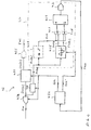
- FIG. 1 shows an embodiment of a switching converter according to the invention.
- the illustrated switching converter is designed as a step-up converter and has input terminals 101, 102 for applying an input voltage Vin, an inductive storage element 10 and a rectifier arrangement 20 connected to the inductive storage element 10.
- the inductive storage element 10 and the rectifier arrangement 20 are in this case connected in series with one another between the input terminals 101, 102.
- the rectifier arrangement 20 has a series connection with a rectifier element 21, for example a diode, and a capacitive storage element 22, for example a capacitor.
- An output voltage Vout of the switching converter for supplying a load Z can be tapped off at output terminals 103, 104 of the rectifier arrangement 20. In the illustrated example, this output voltage Vout corresponds to a voltage across the capacitive storage element 22 of the rectifier arrangement 20.
- a switching arrangement 30 is provided, which is designed to the inductive storage element 10, for example, realized as a storage choke is to magnetize periodically during each magnetization period and then to demagnetize for a demagnetization.
- the switching arrangement 30 has a switching element 31 which is connected in series with the inductive storage element 10 between the input terminals 101, 102 and parallel to the rectifier arrangement 20.
- the switching element 31 When the switching element 31 is activated or closed, the input voltage Vin is applied across the inductive storage element 10, the inductive storage element receives energy via the input terminals 101, 102 and is thereby magnetized.
- the inductive storage element 10 delivers the previously absorbed energy to the rectifier arrangement 20 and is thereby demagnetized.
- the switching arrangement 30 has a drive circuit 32, which generates a drive signal S32, according to which the switching element 31 is triggered to conduct and block.
- the switching element 31 can be realized in particular as a MOS transistor, for example as a MOSFET or IGBT. A load path or drain-source path of such a MOS transistor is in this case connected in series with the inductive storage element 10, a control terminal or gate terminal of this MOS transistor, the drive signal S32 is supplied to conductive and blocking control.
- the control terminal of the switching element 31 may be preceded by a driver circuit 34 which is connected thereto serves to convert signal level of the drive signal S32 to signal levels suitable for driving the switching element.
- the drive circuit 32 periodically actuates the switching element 31, the switching element 31 being turned on during each drive period for one magnetization period and then being blocked for a demagnetization period.
- the demagnetization duration refers to the time duration between a blocking activation of the switching element 31 and a complete demagnetization of the inductive storage element 10.
- a control signal S40 supplied to the control circuit 32 determines the switch-on duration of the switch or the magnetization duration during each activation period, and thus the power consumption of the switch switching converter.
- the drive circuit 32 may be a conventional drive circuit for a switch in a boost converter, so that it is possible to dispense with further embodiments for realizing such a drive circuit.
- the drive circuit 32 may in particular be designed to the step-up converter in the triangular current operation, which is also referred to as discontinuous conduction mode (DCM), or in trapezoidal mode (continuous conduction mode), which is also referred to as continuous current consumption operation operate.
- DCM discontinuous conduction mode
- continuous conduction mode continuous conduction mode
- FIG. 2 shows a time course of a current I in the storage inductor 10 and the drive signal S32 during a drive period in triangular current operation.
- the switching element 31 conducts at a high level of the drive signal S32 and blocks at a low level of this drive signal.
- each drive period Tp comprises a magnetization duration T1 corresponding to the turn-on time of the switching element 31 and a demagnetization duration subsequent to the magnetization duration T1 during which the inductor is completely demagnetized and corresponds to the turn-off duration of the switching element 31.
- the switching element 31 is switched on again at the end of the demagnetization period, ie when the storage inductor 10 is de-energized or demagnetized.
- the drive circuit 32 receives, for example, from an auxiliary coil, which is inductively coupled to the storage inductor.
- a voltage S33 over this auxiliary coil contains information about the instantaneous magnetization state of the storage inductor 10 and thus about times when the inductor 10 is completely demagnetized in each case.
- the switching element 31 is turned on again during the demagnetization, even before the storage inductor is completely demagnetized.
- the input current in this type of control does not drop to zero, in contrast to the triangular current mode.
- the current curve corresponds qualitatively to the current flow in FIG. 2 with the difference that the current does not begin to increase from zero at the beginning of the magnetization duration and does not drop to zero during the demagnetization period.
- a momentarily absorbed power P is proportional to the square of the input voltage, that is to say: P ⁇ Vin 2
- boost converter is used as a power factor correction circuit (Power Factor Controller, PFC) operated.
- PFC Power Factor Controller
- Such a power factor controller is a step-up converter, to which a periodically varying voltage is supplied as input voltage Vin and which generates a DC voltage as output voltage Vout.
- the input voltage Vin is, for example, a sinusoidal-shaped voltage which is generated, for example, by means of a bridge rectifier 50 from a sinusoidal mains voltage Vn.
- such power factor controllers require that the input current, or an average value of the input current, is at least approximately proportional to the input voltage Vin. In triangular current operation, this is ensured if the magnetization duration is the same for successive drive periods and changes only slowly compared to the period of the line voltage.
- the setting of the magnetization duration T1 is effected by the drive circuit 32 in this case depending on the control signal S40.
- the magnetization duration T1 is in a boost converter of the parameters for adjusting the power consumption and thus to control the output voltage Vout. Decreases the output voltage due to an increased power consumption of the load, the duty cycle or magnetization time is increased via the control signal S40 to increase the power consumption and thereby counteract a decrease in the output voltage.
- the condition that the input current should be at least approximately proportional to the input voltage is ensured with reference to equation (7) in a latched switching converter, if the magnetization duration is constant for a number of consecutive drive periods and only slowly compared to the period of the mains voltage Vn changes, and if the proportionality factor p is also constant for a number of consecutive drive periods or changes only slowly compared to the mains voltage Vn.
- the magnetization duration T1 and the proportionality factor p Parameter for changing the power consumption and thus for regulating the output voltage.
- the drive circuit 32 adjusts the magnetization duration T1 and the proportionality factor depending on the control signal S40, wherein the proportionality factor gradually changes with changing control signal, for example, as the magnetization time changes continuously.
- the power consumption is proportional to the square of the input voltage Vin. With a sinusoidal mains voltage, the power consumption thus runs sinusoidally with a frequency which corresponds to twice the mains frequency. These periodic fluctuations of the power consumption are compensated by the rectifier arrangement 20 in order to provide a DC voltage as output voltage Vout at the output 103, 104. Depending on the capacitance value of the output capacitor 22, however, this DC voltage Vout is superimposed by a periodic signal with twice the network frequency. This signal is referred to below as a hum signal whose frequency as hum.
- the switching converter has a regulator arrangement 40 to which the output voltage Vout is supplied.
- this regulator arrangement 40 comprises an error amplifier 414 which generates an error signal or differential signal S41.
- This error signal S41 is a measure of an instantaneous deviation of the output voltage Vout from a setpoint.
- the error amplifier 414 is divided by a voltage divider 411, 412 Output voltage V412 and provided by a reference voltage source 413 reference signal V413, which represents the desired value supplied.
- the error signal S41 in the illustrated switching converter corresponds to a difference between the reference voltage V413 and the divided-down output voltage V412 and is associated with a ripple signal in accordance with the output voltage Vout.
- This error signal S41 is fed to a filter arrangement 42 with a band rejection filter, which is designed to filter out the ripple signal and to provide a filtered error signal S42 at its output.
- the filtered error signal S42 which is ideally no longer having a ripple signal, is fed to a controller 43, which generates the control signal S40 from the filtered error signal S42.
- This controller 43 may have a proportional behavior, the control signal S40 thus generate depending on the instantaneous value of the filtered error signal S42, may have an integral behavior, the control signal S40 thus as a function of the filtered error signal S42 viewed over a predetermined time window in the past generate, or may Proportional-IntegralVerhalten own.
- the filter arrangement 42 has a filter behavior which can be adaptively adapted to the ripple frequency of the ripple signal superimposed on the error signal S41, in order to optimally filter out the ripple signal when the band-stop filter contained in the filter arrangement is as narrow as possible.
- FIG. 4 An embodiment of such an adaptive filter arrangement is shown in FIG. 4 shown.
- This filter arrangement has an analog-to-digital converter 422, to which the error signal S41 is fed and which samples the error signal S41 in time with a clock signal CLK.
- a signal sequence is available, which corresponds to samples of the error signal S41, and which is hereinafter referred to as discrete-time error signal S41 [k].
- This discrete-time error signal S41 [k] is supplied to a band elimination filter 421 which filters the sampled error signal S41 [k] and provides a first filter signal S42 [k], hereinafter also referred to as a band reject filtered error signal.
- FIR Finite Impulse Response
- IIR Infinite Impulse Response
- the band-reject filtered error signal S42 [k] can be output directly as an output signal of the filter arrangement 42 if the subsequent controller 43 is also implemented as a discrete-time controller.
- the filter result is significantly dependent on the sampling frequency.
- the frequency of the signal components filtered out of the error signal S41 by the band elimination filter 421 to obtain the band rejection filtered error signal S42 [k] is dependent on the frequency at which the error signal S41 is sampled.
- the filter arrangement according to FIG. 4 provided to detect the frequency of the hum signal superimposed on the error signal S41 by a frequency measuring arrangement 420 and to adjust the clock frequency of the clock signal CLK depending on the measurement result.
- the frequency measuring arrangement generates for this purpose a clock control signal S420, which is supplied to an oscillator 424.
- This oscillator which is realized for example as a voltage-controlled oscillator, provides the clock signal CLK with a frequency which depends on the clock control signal S420.
- the frequency measuring arrangement 420 may be supplied with the sampled error signal S41 [k] or a signal dependent on the sampled error signal S41 [k].
- a bandpass filter 431 is optionally present, to which the error signal S41 [k] is supplied and at the output of which a band-pass filtered error signal S43 [k] is available, which is supplied to the frequency measuring arrangement 420.
- the filter characteristic of a bandpass filter 431 used to generate the bandpass filtered error signal S43 [k] is complementary to the filter characteristic of the bandstop filter, so that the bandpass filtered error signal S43 [k] represents the signal portion of the error signal S41 [k] which is filtered out by the bandstop filter.
- the frequency measuring arrangement 420 has an evaluation unit 425 to which the band-pass filtered error signal S43 [k] is fed and which determines the frequency of the band-pass filtered error signal S43 [k] with respect to the clock frequency of the clock signal CLK.
- the evaluation unit 425 is supplied in the example for this purpose, a second clock signal CLK '.
- This second clock signal CLK ' is in a fixed relationship to the first clock signal CLK. In particular, it may be identical to the first clock signal CLK or may be proportional in frequency to the first clock signal CLK.
- the second clock signal CLK ' may also be in phase with the first clock signal CLK or out of phase with this first clock signal CLK.
- the frequencies of the clock signals CLK, CLK ' may be lower than an internal clock generated in the voltage controlled oscillator in response to the signal S420.
- a frequency divider (not shown) is integrated, which divides the internally generated clock signal.
- the frequency of this internal clock signal can in this case be in the MHz range, while the frequency of the first and second clock signals CLK, CLK 'is for example in the one-digit kHz range.
- the time-discrete band-pass filtered error signal S43 [k] corresponds to the sampled hum signal.
- This signal S43 [k] is thus a periodic mean-free signal with a frequency corresponding to the ripple frequency. Even if it is assumed that the center of the passband of the bandpass filter 431 or the stop band of the bandstop filter 421 are not exactly matched to the ripple frequency during an adaptation phase, it can nonetheless be assumed that signal components which have the ripple frequency and at least intermittently have a sufficiently high amplitude, the band pass filter 431 happen.
- the evaluation circuit 425 determines, for example, the number of clock periods of the second clock signal CLK 'within a predetermined number of periods of the sampled ripple signal S43 [k]. The start or the end of a period of the ripple signal is recognized by the drive circuit 425, for example, by a change in the polarity of the samples from negative values to positive values.
- frequency measuring arrangement is a discrete-time clock control signal at the output of a controlled by the evaluation circuit 425 counter 429 available.
- This time discrete clock control signal is supplied to a digital-to-analog converter 430, which provides the analog clock control signal S420.
- the drive circuit 425 For controlling the counter 429, the drive circuit 425 generates two control signals 5425_1, S425_2.
- the first control signal S425_1 serves to increment or decrement the counter 429, while the second control signal S425_2 is used to decrement or decrement the counter 429.
- the drive circuit 425 is designed to generate a signal level of the first control signal S425_1 suitable for counting up the counter 429 when the ratio of the clock frequency f CLK to the ripple frequency f B or the Ratio of the period T B of the hum signal and the period T CLK of the clock signal is less than a predetermined limit.
- the counter 429 is counted up to increase the clock frequency of the clock signal CLK via the clock control signal S420.
- the evaluation circuit 425 is configured to generate a signal level of the second control signal S425_2 suitable for decrementing the counter 429 when the ratio of the frequency f CLK of the clock signal and the frequency f B of the hum signal or of the period T B of the hum signal and the period T CLK of the clock signal is greater than a predetermined second threshold.
- the incrementing and decrementing of the counter can be done in equal steps.
- the mode of operation of the evaluation circuit 425 and of the counter 429 for generating the clock control signal S420 can be briefly summarized as follows: Increment counter 420 . if f CLK / f B ⁇ S ⁇ 1 Decrement counter 420 . if f CLK / f B > S ⁇ 2
- S1 and S2 denote limit values of a range of values within which the ratio of clock frequency to ripple frequency should lie.
- the clock frequency f CLK is adjusted via the clock control signal S420 in this case until this condition is met.
- an enabling circuit 426, 427, 428 is provided, which allows incrementing and decrementing the counter 429, and thus a change of the clock control signal S420 only if the amplitude of the bandpass filtered error signal or hum signal S43 [k] is greater than a predetermined amplitude threshold.
- the enable circuit for this purpose comprises a peak rectifier and comparator arrangement 426, which compares the peak value of the ripple signal with the predetermined threshold value and which generates an enable signal S426 only if this peak value lies above the amplitude threshold value.
- the enable circuit also comprises in the illustrated example logic gates 427, 428 formed as AND gates preceding the increment and decrement inputs of the counter 429 and to which the enable signal S426 and the first and second control signals S425_1, S425_2 are applied.
- the control signals 5425_1, S425_2 pass through the logic gates 427, 428 in this enable circuit only to increment or decrement the counter 429 when the enable signal S426 assumes a release level, in the present case a high level.
- the purpose of the enable circuit 426 is to allow adaptation of the filter characteristics above the clock frequency f CLK of the sampling clock only when a ripple signal having a sufficiently high amplitude is present.
- a hum signal small amplitude has little effect on the regulation of power consumption, so that can be dispensed with an exact filtering of such a hum signal small amplitude.
- the bandstop filter 421 has band-stop regions with normalized center frequencies ⁇ 1 and - ⁇ 1.
- Signal components of the sampled hum signal lie in the frequency spectrum at normalized frequencies of - ⁇ 0 ⁇ T CLK and ⁇ 0 ⁇ T CLK .
- the spectral components not equal to zero of the buzz signal can be shifted to the stop bands of the band rejection filter by adjusting the clock frequency f CLK and the clock period T CLK , assuming, of course in that the Nyquist criterion is fulfilled, according to which the sampling frequency must be at least twice as high as the frequency of the sampled signal. That means in the present case: f CLK ⁇ 2 ⁇ f 0 ,
- the operation of the evaluation circuit 425 is described below with reference to FIG. 6 explained. Is shown in FIG. 6 the time profile of the ripple signal sampled at the clock frequency f CLK and the time profile of the clock signal CLK. For this explanation, it is assumed that the clock signal CLK 'supplied to the evaluation circuit 425 corresponds to the clock signal CLK used for sampling the analog signals.
- the evaluation circuit 425 determines the number of clock periods of the clock signal CLK within a predetermined number of periods of the ripple signal, in the example within two periods of the ripple signal.
- the number of clock periods of the clock signal which are within the predetermined number of periods of the hum signal, directly provides a measure of the ratio of clock frequency f CLK to hum frequency f B and can directly for generating the control signals 5425_1, S425_2 for incrementing or decrementing the Counter 429 can be used. If this number of clock periods is below a predetermined limit value, the ratio of clock frequency f CLK to ripple frequency f B is below the first limit value and the clock frequency is too high increase. If this number lies above a further predetermined threshold value, then the ratio of clock frequency F CLK to hum frequency f B is above the second limit value and the clock frequency F CLK is to be correspondingly reduced.
- FIG. 7 An implementation example of an evaluation circuit 425 is in FIG. 7 shown.
- This evaluation circuit has a comparator 441 to which the sampled ripple signal S43 [k] is supplied and which serves to detect a level change of the ripple signal. The individual samples of the mean-free hum signal are compared to zero in order to detect a level change of the hum signal.
- An output signal S441 of this comparator 441 is supplied to a flip-flop 442 which changes state each time the comparison signal S441 rises from a low level to a high level, that is, every new period of the hum signal.
- This "toggle" flip-flop 442 is followed by a counter 443 whose clock input the clock signal CLK or the second clock signal CLK 'is supplied and which is enabled by an output signal S442 of the toggle flip-flop.
- This counter is enabled in the illustrated arrangement at the beginning of every other period of the hum signal and counts during the period of the hum signal, the clock pulses of the clock signal CLK and the second clock signal CLK '.
- the counter is followed by a register 444 which stores at the end of each evaluation period, ie on a falling edge of the flip-flop signal S442, the counter value available at an output of the counter 443.
- the counter value stored in the register 444 which directly represents a measure of the ratio of clock frequency to hum frequency, is compared to first and second threshold values S1, S2 by means of two comparators 445, 446 connected downstream of the register 444.
- the control signals S425_1, S425_2 are available at the outputs of the comparators 445, 446.
- the first control signal S425_1, referring to FIG. 4 incrementing the counter assumes a high level when the number of clock pulses detected during the evaluation period becomes smaller is as a first threshold S1.
- the second clock signal S425_2, referring to FIG. 4 decrements the counter, assumes a high level when the number of detected within the evaluation period clock pulses is greater than a second threshold S2.
- the filter arrangement 42 shown has a band-stop filter for generating the band-stop filtered error signal S42 [k] and a band-pass filter 431 for generating the band-pass filtered error signal S43 [k].
- the functionality of the bandstop filter 421 and the bandpass filter 431, which have mutually complementary transfer functions, can be achieved in a simple manner using a single bandpass filter, as described below with reference to FIG FIG. 9 is explained.
- the bandpass filter 431 in this embodiment is part of the bandstop filter 421 which provides the bandstop filtered error signal S42 [k].
- the bandstop filter 421 in this exemplary embodiment also has a subtracter 432, to which the error signal S41 [k] and a band-pass filtered signal available at the output of the bandpass filter 431 are provided Signal S43 [k] are supplied as input signals.
- the output of the subtracter 432 forms the band rejection filtered error signal S42 [k] and is also applied to the input of the bandpass filter 431, which has a high gain at its resonant frequency in this embodiment.
- the gain of the bandpass filter at its resonant frequency is infinite and depends on a digital realization of rounding errors of the arithmetic units used.
- the filter input signal S41 [k] has frequency components at the resonant frequency of the bandpass filter 431, a signal level arises at its output due to the high gain of the bandpass filter 431, which approximately corresponds to the signal level of the signal component containing the resonance frequency in the input signal S41 [k ], but which has a reverse sign or an opposite phase position, while the signal level of this signal component is significantly reduced in the band rejection filtered signal S42 [k].
- the combination of subtractor 432 and bandpass filter 431 with very high gain acts as a bandstop filter with a gain of about one in the illustrated filter arrangement so that the signal S43 [k] present at the output of the bandpass filter 431 corresponds to a bandpass filtered error signal.
- the frequency of the input signal S41 [k] is slightly adjacent to the resonant frequency of the bandpass filter, then in the steady state at the output of the bandpass filter 431, an oscillation occurs whose amplitude still largely corresponds to the signal amplitude of the input signal S41 [k] and whose phase position is slightly different from that of FIG opposite phase position to the input signal S41 [k] deviates.
- the input signal of the band-pass filter 431 and the band-stop-filtered signal S42 [k] in this case assumes a higher signal level than when excited exactly at the resonance frequency.
- the filter has in terms of its bandpass response, which affects the bandpass filtered signal S43 [k], has a much broader filter characteristic than its band-stop response, which acts on the band-stop signal S42 [k].
- a signal of sufficiently high amplitude is also available for the frequency adjustment at the bandpass output S43 [k] if the filter is not yet exactly matched to the ripple frequency.
Abstract
Description
Die vorliegende Erfindung betrifft einen Schaltwandler, insbesondere einen als Leistungsfaktorkorrekturschaltung (Power Factor Controller, PFC) ausgebildeten Schaltwandler.The present invention relates to a switching converter, in particular a designed as power factor correction circuit (power factor controller, PFC) switching converter.
Eine Leistungsfaktorkorrekturschaltung ist üblicherweise als Hochsetzsteller ausgebildet und umfasst ein induktives Speicherelement, eine an das induktive Speicherelement angeschlossene Gleichrichteranordnung zur Bereitstellung einer Ausgangsspannung und eine an das induktive Speicherelement angeschlossene Schaltanordnung. Die Schaltanordnung regelt die Stromaufnahme des induktiven Speicherelements abhängig von der Ausgangsspannung und ist so verschaltet, dass das Speicherelement periodisch Energie über Eingangsklemmen aufnimmt und dadurch magnetisiert wird, und die aufgenommene Energie anschließend an die Gleichrichteranordnung abgibt und dadurch entmagnetisiert wird.A power factor correction circuit is usually embodied as a step-up converter and comprises an inductive storage element, a rectifier arrangement connected to the inductive storage element for providing an output voltage and a switching arrangement connected to the inductive storage element. The switching arrangement regulates the current consumption of the inductive storage element as a function of the output voltage and is connected so that the storage element periodically absorbs energy via input terminals and is thereby magnetized, and then delivers the absorbed energy to the rectifier arrangement and is thereby demagnetized.
Zur Regelung der Leistungsaufnahme, und damit der Ausgangsspannung, wird bei einem solchen Power Factor Controller ein Regelsignal erzeugt, das abhängig von der Ausgangsspannung ist und das insbesondere die Zeitdauern der Magnetisierungsphasen des induktiven Speicherelements bestimmt. Derartige Power Factor Controller sind beispielsweise beschrieben in der
Weitere Power Factor Controller sind beschrieben in der
Die Eingangsspannung eines Power Factor Controllers ist üblicherweise eine gleichgerichtete Netzspannung und besitzt damit einen sinusbetragförmigen Spannungsverlauf. Die Regelung der Stromaufnahme soll bei einem Power Factor Controller idealerweise so erfolgen, dass ein Mittelwert eines Eingangsstromes proportional ist zu der anliegenden Eingangsspannung. Die Leistungsaufnahme ist dann proportional zum Quadrat der Eingangsspannung und besitzt einen sinusförmigen Verlauf mit einer Frequenz, die der doppelten Netzfrequenz entspricht. Diese zeitlich variierende Leistungsaufnahme führt zu einer Welligkeit der am Ausgang der Gleichrichteranordnung zur Verfügung stehenden Ausgangsspannung, die um so größer ist, je kleiner ein Ausgangskondensator der Gleichrichteranordnung aus Kostengründen dimensioniert wird.The input voltage of a power factor controller is usually a rectified mains voltage and thus has a sinusoidal-shaped voltage curve. The regulation In the case of a power factor controller, the current consumption should ideally be such that an average value of an input current is proportional to the applied input voltage. The power consumption is then proportional to the square of the input voltage and has a sinusoidal profile with a frequency that corresponds to twice the mains frequency. This time-varying power consumption leads to a ripple of the output voltage available at the output of the rectifier arrangement, which is the greater, the smaller an output capacitor of the rectifier arrangement is dimensioned for reasons of cost.
Um zu vermeiden, dass eine solche Welligkeit der Ausgangsspannung die Regelung der Strom- bzw. Leistungsaufnahme beeinflusst, ist es bekannt, in dem Regelkreis ein Bandsperrfilter (Notchfilter) vorzusehen, das Signalanteile mit der doppelten Netzfrequenz ausfiltert. Berücksichtigt man, dass sich die Netzfrequenzen weltweit unterscheiden, so muss der Bandsperrbereich des Filters entsprechend breit gewählt werden, um beispielsweise die 100Hz-Welligkeit eines 50Hz-Netzes und die 120Hz-Welligkeit eines 60Hz-Netzes sicher auszufiltern. Allerdings verschlechtern sich die Eigenschaften eines solchen Filters bezüglich Dämpfung und Gruppenlaufzeit mit zunehmender Breite der Bandsperre.In order to avoid that such an output voltage ripple influences the regulation of the current or power consumption, it is known to provide in the control loop a notch filter which filters out signal components at twice the mains frequency. If one considers that the mains frequencies differ worldwide, then the band-stop range of the filter must be chosen correspondingly broad, for example to reliably filter out the 100 Hz ripple of a 50 Hz network and the 120 Hz ripple of a 60 Hz network. However, the properties of such a filter with respect to attenuation and group delay deteriorate with increasing width of the bandstop filter.
Bei digitalen Filtern ist darüber hinaus ein ausreichend genauer Takt zum Abtasten des zu filternden Signals erforderlich, da die Filtercharakteristik ansonsten den Toleranzen des Taktsignals unterliegt.Moreover, with digital filters, a sufficiently accurate clock is required to sample the signal to be filtered, since the filter characteristic is otherwise subject to the tolerances of the clock signal.
Die Welligkeit der Ausgangsspannung kann auch dadurch eliminiert werden, dass die Ausgangsspannung zum Zweck der Regelung der Leistungsaufnahme über ein gegebenes Zeitfenster gemittelt wird. Dies verlangsamt allerdings die Regelung und beeinträchtigt die Fähigkeit des Schaltwandlers, auf Lastsprünge am Ausgang rasch zu reagieren.The ripple of the output voltage can also be eliminated by averaging the output voltage for the purpose of regulating the power consumption over a given time window. However, this slows down the control and affects the ability of the switching converter to respond quickly to load transients at the output.
In
Aufgabe der vorliegenden Erfindung ist es, einen Schaltwandler, insbesondere einen als Leistungsfaktorkorrekturschaltung ausgebildeten Schaltwandler zur Verfügung zu stellen, der aus einer Eingangsspannung eine geregelte Ausgangsspannung für eine Last erzeugt, der auf Lastsprünge der Last rasch reagieren kann und bei dem ein Einfluss einer aus der Eingangsspannung resultierenden Welligkeit der Ausgangsspannung auf die Regelung der Ausgangsspannung reduziert ist.The object of the present invention is to provide a switching converter, in particular a switching converter designed as a power factor correction circuit, which generates from an input voltage a regulated output voltage for a load which can respond rapidly to load transients of the load and at which an influence of the input voltage resulting ripple of the output voltage is reduced to the regulation of the output voltage.
Diese Aufgabe wird durch einen Schaltwandler nach Anspruch 1 gelöst. Ausgestaltungen der Erfindung sind Gegenstand der Unteransprüche.This object is achieved by a switching converter according to
Ein Schaltwandler gemäß einem Ausführungsbeispiel der Erfindung umfasst ein induktives Energiespeicherelement, eine an das induktive Energiespeicherelement angeschlossene Gleichrichteranordnung mit Ausgangsklemmen zur Bereitstellung einer Ausgangsspannung, eine Schaltanordnung zur Regelung einer Stromaufnahme des induktiven Energiespeicherelements abhängig von einem Regelsignal und eine Regleranordnung, die dazu ausgebildet ist, das Regelsignal abhängig von der Ausgangsspannung zu erzeugen. Die Regleranordnung umfasst ein diskretes Bandsperrfilter, dem ein von der Ausgangsspannung abhängiges, nach Maßgabe eines Taktsignals abgetastetes Fehlersignal und das Taktsignal zugeführt sind und das ein erstes Filtersignal erzeugt, von dem das Regelsignal abhängig ist, eine Frequenzmessanordnung, der das Fehlersignal zugeführt ist und die dazu ausgebildet ist, eine Frequenz eines periodischen Signalanteils des Fehlersignals zu ermitteln und ein von dieser Frequenz abhängiges Taktsteuersignal zu erzeugen, und einen steuerbaren Oszillator, dem das Taktsteuersignal zugeführt ist und der das Taktsignal abhängig von dem Taktsteuersignal erzeugt.A switching converter according to an embodiment of the invention comprises an inductive energy storage element, a connected to the inductive energy storage element rectifier arrangement with output terminals for providing an output voltage, a switching arrangement for controlling a current consumption of the inductive energy storage element depending on a control signal and a controller arrangement, which is adapted to the control signal depending on the output voltage. The controller arrangement comprises a discrete band-stop filter, to which an error signal dependent on the output voltage and the clock signal are fed and which generates a first filter signal on which the control signal is dependent, a frequency measuring arrangement to which the error signal is fed and which thereto is designed to determine a frequency of a periodic signal component of the error signal and one of these Frequency dependent clock control signal to generate, and a controllable oscillator to which the clock control signal is supplied and which generates the clock signal in response to the clock control signal.
Die Frequenzmessanordnung ermöglicht bei diesem Schaltwandler eine adaptive Anpassung der Abtastfrequenz an die nachfolgend als Brummfrequenz bezeichnete Frequenz eines periodischen Signalanteils des Fehlersignals. Hierdurch kann die Brummfrequenz in den Bandsperrbereich des Bandsperrfilters verschoben werden, so dass ein Filter mit einem schmalen Sperrbereich verwendet werden kann.In this switching converter, the frequency measuring arrangement allows an adaptive adaptation of the sampling frequency to the frequency of a periodic signal component of the error signal, referred to below as the ripple frequency. This allows the ripple frequency to be shifted to the band stop region of the band reject filter, so that a filter having a narrow stop band can be used.
Ausführungsbeispiele der vorliegenden Erfindung werden nachfolgend anhand von Figuren erläutert. In diesem Zusammenhang sei darauf hingewiesen, dass in den Figuren lediglich die zum Verständnis der Erfindung erforderlichen Schaltungskomponenten dargestellt sind.
Figur 1- zeigt ein Ausführungsbeispiel eines erfindungsgemäßen Schaltwandlers, der als Hochsetzsteller ausgebildet ist und der einen Rückkopplungszweig mit einer adaptiv einstellbaren, ein Bandsperrfilter aufweisenden Filteranordnung aufweist.
Figur 2- veranschaulicht die Funktionsweise eines nichtlückend betriebenen Hochsetzstellers.
- Figur 3
- veranschaulicht die Funktionsweise eines lückend betriebenen Hochsetzstellers.
Figur 4- zeigt ein Realisierungsbeispiel der adaptiven Filteranordnung.
Figur 5- veranschaulicht Frequenzgänge eines bandpassgefilterten Fehlersignals sowie einer Übertragungsfunktion des Bandsperrfilters zur Erläuterung der Funktionsweise der adaptiven Filteranordnung.
- Figur 6
- veranschaulicht die Funktionsweise einer in der Frequenzmessanordnung vorhandenen Auswerteschaltung anhand von Signalverläufen.
- Figur 7
- zeigt ein Ausführungsbeispiel der Auswerteschaltung.
- Figur 8
- zeigt ausschnittsweise eine Abwandlung der Auswerteschaltung gemäß
Figur 7 . - Figur 9
- zeigt ein Realisierungsbeispiel für ein Bandsperrfilter und ein Bandpassfilter der Filteranordnung.
- FIG. 1
- shows an embodiment of a switching converter according to the invention, which is designed as a step-up converter and having a feedback path with an adaptively adjustable, a notch filter having filter assembly.
- FIG. 2
- illustrates the operation of a non-latching operated boost converter.
- FIG. 3
- illustrates the operation of a latching operated boost converter.
- FIG. 4
- shows an implementation example of the adaptive filter arrangement.
- FIG. 5
- illustrates frequency responses of a bandpass filtered error signal and a transfer function the band-stop filter to explain the operation of the adaptive filter assembly.
- FIG. 6
- illustrates the operation of an existing in the frequency measurement arrangement evaluation circuit based on signal waveforms.
- FIG. 7
- shows an embodiment of the evaluation circuit.
- FIG. 8
- shows a detail of a modification of the evaluation circuit according to
FIG. 7 , - FIG. 9
- shows an implementation example of a band rejection filter and a bandpass filter of the filter assembly.
In den Figuren bezeichnen, sofern nicht anders angegeben, gleiche Bezugszeichen gleiche Schaltungskomponenten und Signale mit gleicher Bedeutung.In the figures, unless otherwise stated, like reference numerals designate like circuit components and signals having the same meaning.
Zur Regelung einer Stromaufnahme des induktiven Speicherelements 10, somit zur Regelung der Leistungsaufnahme über die Eingangsklemmen 101, 102 und somit zur Regelung der Ausgangsspannung Vout des Schaltwandlers ist eine Schaltanordnung 30 vorhanden, die dazu ausgebildet ist, das induktive Speicherelement 10, das beispielsweise als Speicherdrossel realisiert ist, periodisch jeweils während einer Magnetisierungsdauer zu magnetisieren und anschließend für eine Entmagnetisierungsdauer zu entmagnetisieren. Die Schaltanordnung 30 weist hierzu ein Schaltelement 31 auf, das in Reihe zu dem induktiven Speicherelement 10 zwischen die Eingangsklemmen 101, 102 und das parallel zu der Gleichrichteranordnung 20 geschaltet ist. Bei leitend angesteuertem bzw. geschlossenem Schaltelement 31 liegt die Eingangsspannung Vin über dem induktiven Speicherelement 10 an, das induktive Speicherelement nimmt dabei Energie über die Eingangsklemmen 101, 102 auf und wird dadurch magnetisiert. Bei anschließend sperrend angesteuertem bzw. geöffnetem Schaltelement 31 gibt das induktive Speicherelement 10 die zuvor aufgenommene Energie an die Gleichrichteranordnung 20 ab und wird dadurch entmagnetisiert.For regulating a current consumption of the
Zur Ansteuerung des Schaltelements 31 weist die Schaltanordnung 30 eine Ansteuerschaltung 32 auf, die ein Ansteuersignal S32 erzeugt, nach dessen Maßgabe das Schaltelement 31 leitend und sperrend angesteuert ist. Das Schaltelement 31 kann insbesondere als MOS-Transistor, beispielsweise als MOSFET oder IGBT realisiert sein. Eine Laststrecke bzw. Drain-Source-Strecke eines solchen MOS-Transistors ist hierbei in Reihe zu dem induktiven Speicherelement 10 geschaltet, einem Steueranschluss bzw. Gate-Anschluss dieses MOS-Transistors ist das Ansteuersignal S32 zu leitenden und sperrenden Ansteuerung zugeführt. Optional kann dem Steueranschluss des Schaltelements 31 eine Treiberschaltung 34 vorgeschaltet sein, die dazu dient, Signalpegel des Ansteuersignals S32 auf zur Ansteuerung des Schaltelements geeignete Signalpegel umzusetzen.For driving the switching element 31, the switching
Die Ansteuerschaltung 32 steuert das Schaltelement 31 periodisch an, wobei das Schaltelement 31 während jeder Ansteuerperiode für eine Magnetisierungsdauer leitend und anschließend für eine Entmagnetisierungsdauer sperrend angesteuert wird. Die Entmagnetisierungsdauer bezeichnet hierbei die Zeitdauer zwischen einer sperrenden Ansteuerung des Schaltelements 31 und einer vollständigen Entmagnetisierung des induktiven Speicherelements 10. Ein der Ansteuerschaltung 32 zugeführtes Regelsignal S40 bestimmt bei diesem Schaltwandler die Einschaltdauer des Schalters bzw. die Magnetisierungsdauer während jeder Ansteuerperiode, und damit die Leistungsaufnahme des Schaltwandlers. Die Ansteuerschaltung 32 kann eine herkömmliche Ansteuerschaltung für einen Schalter in einem Hochsetzsteller sein, so dass auf weitere Ausführungen zur Realisierung einer solchen Ansteuerschaltung verzichtet werden kann.The
Die Ansteuerschaltung 32 kann insbesondere dazu ausgebildet sein, den Hochsetzsteller im Dreieckstrombetrieb, der auch als Betrieb mit diskontinuierlicher Stromaufnahme (Discontinuous Conduction Mode, DCM) bezeichnet wird, oder im Trapezstrombetrieb (Continuous Conduction Mode), der auch als Betrieb mit kontinuierlicher Stromaufnahme bezeichnet wird zu betreiben.The
Bezugnehmend auf
Im Trapezstrombetrieb, für den die Signalverläufe in
Bei beiden zuvor erläuterten Betriebsarten ist eine momentan aufgenommene Leistung P proportional zum Quadrat der Eingangsspannung, es gilt also: 
Der in
Zur Minimierung der Blindleistung zur Aufnahme aus dem Netz ist bei solchen Power Factor Controllern gefordert, dass der Eingangsstrom, bzw. ein Mittelwert des Eingangsstroms, wenigstens annäherungsweise proportional ist zu der Eingangsspannung Vin. Im Dreieckstrombetrieb ist dies gewährleistet, wenn die Magnetisierungsdauer für aufeinanderfolgende Ansteuerperioden gleich ist und sich nur langsam im Vergleich zur Periodendauer der Netzspannung ändert. Die Einstellung der Magnetisierungsdauer T1 erfolgt durch die Ansteuerschaltung 32 hierbei abhängig von dem Regelsignal S40. Die Magnetisierungsdauer T1 ist bei einem Hochsetzsteller der Parameter zur Einstellung der Leistungsaufnahme und damit zur Regelung der Ausgangsspannung Vout. Sinkt die Ausgangsspannung bedingt durch eine erhöhte Leistungsaufnahme der Last, so wird über das Regelsignal S40 die Einschaltdauer bzw. Magnetisierungsdauer vergrößert, um die Leistungsaufnahme zu erhöhen und dadurch einem Absinken der Ausgangsspannung entgegenzuwirken.In order to minimize the reactive power required to be taken out of the grid, such power factor controllers require that the input current, or an average value of the input current, is at least approximately proportional to the input voltage Vin. In triangular current operation, this is ensured if the magnetization duration is the same for successive drive periods and changes only slowly compared to the period of the line voltage. The setting of the magnetization duration T1 is effected by the
Die Bedingung, dass der Eingangsstrom wenigstens annähernd proportional zu der Eingangsspannung sein soll, ist Bezug nehmend auf Gleichung (7) bei einem lückend betriebenen Schaltwandler gewährleistet, wenn die Magnetisierungsdauer für eine Anzahl aufeinanderfolgender Ansteuerperioden konstant ist und sich nur langsam im Vergleich zur Periodendauer der Netzspannung Vn ändert, und wenn der Proportionalitätsfaktor p ebenfalls für eine Anzahl aufeinanderfolgender Ansteuerperioden konstant ist bzw. sich nur langsam im Vergleich zu der Netzspannung Vn ändert. In einem lückend betriebenen Schaltwandler sind die Magnetisierungsdauer T1 und der Proportionalitätsfaktor p Parameter zur Änderung der Leistungsaufnahme und damit zur Regelung der Ausgangsspannung. Steigt beispielsweise die Ausgangsspannung in Folge einer verringerten Leistungsaufnahme der Last Z, so wird beispielsweise die Magnetisierungsdauer verkleinert und/oder die Wartezeit verlängert, um dadurch die Leistungsaufnahme zu verringern und einem Anstieg der Ausgangsspannung entgegenzuwirken. Bei lückendem Betrieb stellt die Ansteuerschaltung 32 die Magnetisierungsdauer T1 und den Proportionalitätsfaktor abhängig von dem Regelsignal S40 ein, wobei der Proportionalitätsfaktor sich mit änderndem Regelsignal beispielsweise stufenweise ändert, während die Magnetisierungsdauer sich stetig ändert.The condition that the input current should be at least approximately proportional to the input voltage is ensured with reference to equation (7) in a latched switching converter, if the magnetization duration is constant for a number of consecutive drive periods and only slowly compared to the period of the mains voltage Vn changes, and if the proportionality factor p is also constant for a number of consecutive drive periods or changes only slowly compared to the mains voltage Vn. In a gap-operated switching converter are the magnetization duration T1 and the proportionality factor p Parameter for changing the power consumption and thus for regulating the output voltage. If, for example, the output voltage increases as a result of a reduced power consumption of the load Z, then for example the magnetization duration is reduced and / or the waiting time is lengthened, thereby reducing the power consumption and counteracting an increase in the output voltage. In the case of a lopsided operation, the
Bezug nehmend auf die Gleichungen (4) und (7) ist die Leistungsaufnahme proportional zum Quadrat der Eingangsspannung Vin. Bei einer sinusförmigen Netzspannung verläuft die Leistungsaufnahme damit sinusförmig mit einer Frequenz, die der doppelten Netzfrequenz entspricht. Diese periodischen Schwankungen der Leistungsaufnahme werden durch die Gleichrichteranordnung 20 ausgeglichen, um am Ausgang 103, 104 eine Gleichspannung als Ausgangsspannung Vout zur Verfügung zu stellen. Abhängig vom Kapazitätswert des Ausgangskondensators 22 ist dieser Gleichspannung Vout jedoch ein periodisches Signal mit der doppelten Netzfrequenz überlagert. Dieses Signal wird nachfolgend als Brummsignal bezeichnet, dessen Frequenz als Brummfrequenz.Referring to equations (4) and (7), the power consumption is proportional to the square of the input voltage Vin. With a sinusoidal mains voltage, the power consumption thus runs sinusoidally with a frequency which corresponds to twice the mains frequency. These periodic fluctuations of the power consumption are compensated by the
Zur Erzeugung des die Leistungsaufnahme regelnden Regelsignals S40 weist der Schaltwandler eine Regleranordnung 40 auf, der die Ausgangsspannung Vout zugeführt ist. Diese Regleranordnung 40 umfasst in dem dargestellten Beispiel einen Fehlerverstärker 414, der ein Fehlersignal bzw. Differenzsignal S41 erzeugt. Dieses Fehlersignal S41 ist ein Maß für eine momentane Abweichung der Ausgangsspannung Vout von einem Sollwert. Zur Erzeugung des Fehlersignals S41 ist dem Fehlerverstärker 414 eine durch einen Spannungsteiler 411, 412 heruntergeteilte Ausgangsspannung V412 und ein durch eine Referenzspannungsquelle 413 bereitgestelltes Referenzsignal V413, das den Sollwert repräsentiert, zugeführt. Das Fehlersignal S41 entspricht bei dem dargestellten Schaltwandler einer Differenz zwischen der Referenzspannung V413 und der heruntergeteilten Ausgangsspannung V412 und ist entsprechend der Ausgangsspannung Vout mit einem Brummsignal behaftet. Dieses Fehlersignal S41 ist einer Filteranordnung 42 mit einem Bandsperrfilter zugeführt, die dazu ausgebildet ist, das Brummsignal auszufiltern und ein gefiltertes Fehlersignal S42 an ihrem Ausgang zur Verfügung zu stellen. Das gefilterte, idealerweise kein Brummsignal mehr aufweisende, Fehlersignal S42 ist einem Regler 43 zugeführt, der das Regelsignal S40 aus dem gefilterten Fehlersignal S42 erzeugt. Dieser Regler 43 kann ein Proportionalverhalten besitzen, das Regelsignal S40 also abhängig von dem Momentanwert des gefilterten Fehlersignals S42 erzeugen, kann ein Integralverhalten besitzen, das Regelsignal S40 also abhängig von dem gefilterten Fehlersignal S42 betrachtet über ein vorgegebenes Zeitfensters in der Vergangenheit erzeugen, oder kann ein Proportional-IntegralVerhalten besitzen.To generate the power consumption regulating control signal S40, the switching converter has a
Die Filteranordnung 42 besitzt ein Filterverhalten, das adaptiv an die Brummfrequenz des dem Fehlersignal S41 überlagerten Brummsignals angepasst werden kann, um bei einer möglichst schmalen Bandsperre des in der Filteranordnung enthaltenen Bandsperrfilters das Brummsignal optimal auszufiltern.The
Ein Ausführungsbeispiel einer solchen adaptiven Filteranordnung ist in
Bei einer gegebenen Bandsperrcharakteristik des zeitdiskreten Bandsperrfilters 421 ist das Filterergebnis maßgeblich von der Abtastfrequenz abhängig. Die Frequenz der Signalanteile, die aus dem Fehlersignal S41 durch das Bandsperrfilter 421 ausgefiltert werden, um das bandsperrgefilterte Fehlersignal S42[k] zu erhalten, ist abhängig von der Frequenz, mit der das Fehlersignal S41 abgetastet wird. Um einerseits ein Bandsperrfilter mit einem schmalen Sperrbereich verwenden zu können, das Brummsignal andererseits jedoch optimal auszufiltern bzw. zu dämpfen, ist bei der Filteranordnung gemäß
Die Frequenzmessanordnung erzeugt hierzu ein Taktsteuersignal S420, das einem Oszillator 424 zugeführt ist. Dieser Oszillators, der beispielsweise als spannungsgesteuerter Oszillator realisiert ist, stellt das Taktsignal CLK mit einer von dem Taktsteuersignal S420 abhängigen Frequenz zur Verfügung.The frequency measuring arrangement generates for this purpose a clock control signal S420, which is supplied to an
Zur Erzeugung des Taktsteuersignals S420 kann der Frequenzmessanordnung 420 das abgetastete Fehlersignal S41[k] oder ein von dem abgetasteten Fehlersignal S41[k] abhängiges Signal zugeführt sein. Bei der dargestellten Anordnung ist optional ein Bandpassfilter 431 vorhanden, dem das Fehlersignal S41[k] zugeführt ist und an dessen Ausgang ein bandpassgefiltertes Fehlersignal S43[k] zur Verfügung steht, das der Frequenzmessanordnung 420 zugeführt ist. Die Filtercharakteristik eines zur Erzeugung des bandpassgefilterten Fehlersignals S43[k] verwendeten Bandpassfilters 431 ist komplementär zu der Filtercharakteristik des Bandsperrfilters, so dass das bandpassgefilterte Fehlersignal S43[k] den Signalanteil des Fehlersignals S41[k] repräsentiert, der durch das Bandsperrfilter ausgefiltert wird. Die Frequenzmessanordnung 420 weist eine Auswerteeinheit 425 auf, der das bandpassgefilterte Fehlersignal S43[k] zugeführt ist und die die Frequenz des bandpassgefilterten Fehlersignals S43[k] in Bezug auf die Taktfrequenz des Taktsignals CLK ermittelt. Der Auswerteeinheit 425 ist in dem Beispiel hierzu ein zweites Taktsignal CLK' zugeführt. Dieses zweite Taktsignal CLK' steht in einer festen Beziehung zu dem ersten Taktsignal CLK. Es kann insbesondere identisch mit dem ersten Taktsignal CLK sein oder kann hinsichtlich der Frequenz proportional zu dem ersten Taktsignal CLK sein. Das zweite Taktsignal CLK' kann außerdem in Phase zu dem ersten Taktsignal CLK oder phasenverschoben zu diesem ersten Taktsignal CLK sein.To generate the clock control signal S420, the
Die Frequenzen der Taktsignale CLK, CLK' können geringer sein, als ein in dem spannungesteuerten Oszillator abhängig von dem Signal S420 erzeugter interner Takt. In dem Oszillator ist in diesem Fall ein Frequenzteiler (nicht dargestellt) integriert, der das intern erzeugte Taktsignal herunterteilt. Die Frequenz dieses internen Taktsignals kann hierbei im MHz-Bereich liegen, während die Frequenz der ersten und zweiten Taktsignale CLK, CLK' beispielsweise im einstelligen kHz-Bereich liegt.The frequencies of the clock signals CLK, CLK 'may be lower than an internal clock generated in the voltage controlled oscillator in response to the signal S420. In the oscillator in this case, a frequency divider (not shown) is integrated, which divides the internally generated clock signal. The frequency of this internal clock signal can in this case be in the MHz range, while the frequency of the first and second clock signals CLK, CLK 'is for example in the one-digit kHz range.
Für die nachfolgende Erläuterung wird davon ausgegangen, dass das zeitdiskrete bandpassgefilterte Fehlersignal S43[k] dem abgetasteten Brummsignal entspricht. Dieses Signal S43[k] ist somit ein periodisches mittelwertfreies Signal mit einer der Brummfrequenz entsprechenden Frequenz. Selbst wenn davon ausgegangen wird, dass die Mitte des Durchlassbereiches des Bandpassfilters 431 bzw. des Sperrbereiches des Bandsperrfilters 421 während einer Adaptionsphase nicht exakt an die Brummfrequenz angepasst sind, so kann dennoch davon ausgegangen werden, dass zumindest zeitweise Signalanteile, die die Brummfrequenz aufweisen und die eine ausreichend hohe Amplitude besitzen, das Bandpassfilter 431 passieren.For the following explanation, it is assumed that the time-discrete band-pass filtered error signal S43 [k] corresponds to the sampled hum signal. This signal S43 [k] is thus a periodic mean-free signal with a frequency corresponding to the ripple frequency. Even if it is assumed that the center of the passband of the
Zur Ermittlung eines Verhältnisses zwischen der Brummfrequenz und der Taktfrequenz fCLK ermittelt die Auswerteschaltung 425 beispielsweise die Anzahl der Taktperioden des zweiten Taktsignals CLK' innerhalb einer vorgegebenen Anzahl von Perioden des abgetasteten Brummsignals S43[k]. Der Beginn bzw. das Ende einer Periode des Brummsignals wird durch die Ansteuerschaltung 425 beispielsweise dadurch erkannt, dass ein Wechsel der Polarität der Abtastwerte von negativen Werten zu positiven Werten vorliegt.To determine a ratio between the ripple frequency and the clock frequency f CLK, the
Bei der in
Das Inkrementieren und Dekrementieren des Zählers kann in jeweils gleichen Schritten erfolgen. Darüber hinaus besteht auch die Möglichkeit, den Wert, um den der Zähler 429 jeweils inkrementiert oder dekrementiert wird, abhängig davon einzustellen, wie stark das Verhältnis von Taktfrequenz fCLK zu Brummfrequenz fB von einem gewünschten Wertebereich abweicht. Die Funktionsweise der Auswerteschaltung 425 und des Zählers 429 zur Erzeugung des Taktsteuersignals S420 kann wie folgt kurz zusammengefasst werden: ![]()
![]()
![]()
![]()
S1 und S2 bezeichnen hierbei Grenzwerte eines Wertebereiches, innerhalb dessen das Verhältnis aus Taktfrequenz zu Brummfrequenz liegen soll. Die Taktfrequenz fCLK wird über das Taktsteuersignal S420 hierbei solange angepasst, bis diese Bedingung erfüllt ist.Here, S1 and S2 denote limit values of a range of values within which the ratio of clock frequency to ripple frequency should lie. The clock frequency f CLK is adjusted via the clock control signal S420 in this case until this condition is met.
Optional ist bei der in
Die Funktionsweise der in ![]()
![]()
Die Funktionsweise der Auswerteschaltung 425 wird nachfolgend anhand von
Ein Realisierungsbeispiel einer Auswerteschaltung 425 ist in
Eine Auswertung der Anzahl der Taktimpulse über mehrere Perioden des Brummsignals ist möglich, wenn das Flipflop 442 durch einen Zähler ersetzt wird, dessen Takteingang das Vergleichssignal S441 zugeführt ist und der den nachgeschalteten Zähler 443 freigibt. Eine Auswertung über zwei Ansteuerperioden des Brummsignals lässt sich beispielsweise mittels eines 2-Bit-Zählers erreichen, dessen Bits durch ein XOR-Gatter verknüpft, das Freigabesignal S442 bilden. Bei dieser Anordnung ist der Zähler 443 jeweils dann freigegeben, wenn der Zählerstand des vorgeschalteten Zählers 1 oder 2 beträgt. Eine derartige Zähleranordnung als Ersatz für das Flipflop 442 ist in
Bei der in
Das Bandpassfilter 431 ist bei dieser Ausführungsform Teil des Bandsperrfilters 421, das das bandsperrgefilterte Fehlersignal S42[k] bereitstellt. Das Bandsperrfilter 421 weist bei diesem Ausführungsbeispiel außerdem einen Subtrahierer 432 auf, dem das Fehlersignal S41[k] und ein am Ausgang des Bandpassfilters 431 zur Verfügung stehendes bandpassgefilterte Signal S43[k] als Eingangssignale zugeführt sind. Das Ausgangssignal des Subtrahierers 432 bildet das bandsperrgefilterte Fehlersignal S42[k] und ist außerdem dem Eingang des Bandpassfilters 431 zugeführt, das in diesem Ausführungsbeispiel bei seiner Resonanzfrequenz eine hohe Verstärkung aufweist. Im Idealfall ist die Verstärkung des Bandpassfilters bei seiner Resonanzfrequenz unendlich und hängt bei einer digitalen Realisierung von Rundungsfehlern der dabei verwendeten Rechenwerke ab.The
Weist das Filtereingangssignal S41[k] Frequenzanteile bei der Resonanzfrequenz des Bandpassfilters 431 auf, so stellt sich bedingt durch die hohe Verstärkung des Bandpassfilters 431 an dessen Ausgang ein Signalpegel ein, der in etwa dem Signalpegel des die Resonanzfrequenz aufweisenden Signalanteils in dem Eingangssignal S41[k] entspricht, der jedoch ein umgekehrtes Vorzeichen bzw. eine entgegen gesetzte Phasenlage aufweist, während der Signalpegel dieses Signalanteils in dem bandsperrgefilterten Signal S42[k] deutlich reduziert ist. Die Kombination aus Subtrahierer 432 und Bandpassfilter 431 mit sehr hoher Verstärkung wirkt bei der dargestellten Filteranordnung wie ein Bandsperrfilter mit einem Verstärkungsfaktor von etwa Eins, so dass das am Ausgang des Bandpassfilters 431 anliegende Signal S43[k] einem bandpassgefilterten Fehlersignal entspricht.If the filter input signal S41 [k] has frequency components at the resonant frequency of the
Liegt die Frequenz des Eingangssignals S41[k] etwas neben der Resonanzfrequenz des Bandpassfilters, so stellt sich im eingeschwungenen Zustand am Ausgang des Bandpassfilters 431 eine Schwingung ein, deren Amplitude noch weitgehend der Signalamplitude des Eingangssignals S41[k] entspricht und deren Phasenlage etwas von der entgegen gesetzten Phasenlage zum Eingangssignal S41[k] abweicht. Das Eingangssignal des Bandpassfilters 431 bzw. das bandsperrgefilterte Signal S42[k] nimmt in diesem Fall einen höheren Signalpegel an als bei Anregung exakt auf der Resonanzfrequenz. Das Filter weist also bezüglich seines Bandpassverhaltens, das sich auf das bandpassgefilterte Signal S43[k] auswirkt, eine wesentlich breitere Filtercharakteristik auf als bezüglich seines Bandsperrverhaltens, das sich auf das Bandsperrsignal S42[k] auswirkt. Dadurch steht, wie zuvor beschrieben, auch dann ein Signal genügend hoher Amplitude für die Frequenzeinstellung an dem Bandpassausgang S43[k] zur Verfügung, wenn das Filter noch nicht exakt auf die Brummfrequenz abgestimmt ist.If the frequency of the input signal S41 [k] is slightly adjacent to the resonant frequency of the bandpass filter, then in the steady state at the output of the
Claims (11)
bei dem die Auswerteschaltung abhängig von dem Verhältnis zwischen der Periodendauer des periodischen Signalanteils des Fehlersignals (S41[k]) und der Periodendauer des Taktsignals (CLK) wenigstens ein Steuersignal (S425_1, S425_2) erzeugt,
bei dem das wenigstens eine Steuersignal (S425_1, S425_2) einer Taktsteuersignalerzeugungsschaltung (429, 430) zugeführt ist, die das Taktsteuersignal (S420) abhängig von dem wenigstens einen Steuersignal (S425_1, S425_2) bereitstellt.Switching converter according to claim 4 or 5,
in which the evaluation circuit generates at least one control signal (S425_1, S425_2) as a function of the ratio between the period of the periodic signal component of the error signal (S41 [k]) and the period of the clock signal (CLK),
in which the at least one control signal (S425_1, S425_2) is supplied to a clock control signal generation circuit (429, 430) which provides the clock control signal (S420) in dependence on the at least one control signal (S425_1, S425_2).
Priority Applications (2)
| Application Number | Priority Date | Filing Date | Title |
|---|---|---|---|
| EP07002759A EP1956701B1 (en) | 2007-02-08 | 2007-02-08 | DC/DC-converter with a band pass filter and a band rejection filter in the voltage control loop |
| US12/028,488 US7894218B2 (en) | 2007-02-08 | 2008-02-08 | Switch-mode converter |
Applications Claiming Priority (1)
| Application Number | Priority Date | Filing Date | Title |
|---|---|---|---|
| EP07002759A EP1956701B1 (en) | 2007-02-08 | 2007-02-08 | DC/DC-converter with a band pass filter and a band rejection filter in the voltage control loop |
Publications (2)
| Publication Number | Publication Date |
|---|---|
| EP1956701A1 true EP1956701A1 (en) | 2008-08-13 |
| EP1956701B1 EP1956701B1 (en) | 2012-03-28 |
Family
ID=38308741
Family Applications (1)
| Application Number | Title | Priority Date | Filing Date |
|---|---|---|---|
| EP07002759A Active EP1956701B1 (en) | 2007-02-08 | 2007-02-08 | DC/DC-converter with a band pass filter and a band rejection filter in the voltage control loop |
Country Status (2)
| Country | Link |
|---|---|
| US (1) | US7894218B2 (en) |
| EP (1) | EP1956701B1 (en) |
Cited By (2)
| Publication number | Priority date | Publication date | Assignee | Title |
|---|---|---|---|---|
| WO2012002824A2 (en) * | 2010-06-29 | 2012-01-05 | Eaton Industries Company | Closed loop control of a cyclo-converter |
| TWI786210B (en) * | 2017-10-30 | 2022-12-11 | 美商瑞薩電子美國有限公司 | Preserving phase interleaving in a hysteretic multiphase buck controller |
Families Citing this family (11)
| Publication number | Priority date | Publication date | Assignee | Title |
|---|---|---|---|---|
| TWM359870U (en) * | 2008-12-31 | 2009-06-21 | Princeton Technology Corp | A sensing type control circuit for appliance loading |
| WO2010144166A1 (en) * | 2009-06-12 | 2010-12-16 | University Of Florida Research Foundation Inc. | Electromechanical inductors and transformers |
| TWI452810B (en) * | 2011-11-08 | 2014-09-11 | Richtek Technology Corp | Mixed mode compensation circuit and method for a power converter |
| US9395738B2 (en) | 2013-01-28 | 2016-07-19 | Nvidia Corporation | Current-parking switching regulator with a split inductor |
| US9800158B2 (en) | 2013-01-30 | 2017-10-24 | Nvidia Corporation | Current-parking switching regulator downstream controller |
| US9804621B2 (en) * | 2013-02-05 | 2017-10-31 | Nvidia Corporation | Current-parking switching regulator downstream controller pre-driver |
| US9459635B2 (en) * | 2013-02-08 | 2016-10-04 | Nvidia Corporation | Current-parking switching regulator upstream controller |
| US9389617B2 (en) | 2013-02-19 | 2016-07-12 | Nvidia Corporation | Pulsed current sensing |
| US9639102B2 (en) | 2013-02-19 | 2017-05-02 | Nvidia Corporation | Predictive current sensing |
| US8976898B1 (en) * | 2013-11-14 | 2015-03-10 | Lsi Corporation | Low-distortion class S power amplifier with constant-impedance bandpass filter |
| TWI806548B (en) * | 2022-04-13 | 2023-06-21 | 宏碁股份有限公司 | Boost converter |
Citations (2)
| Publication number | Priority date | Publication date | Assignee | Title |
|---|---|---|---|---|
| DE2158105A1 (en) * | 1971-11-24 | 1973-05-30 | Wandel & Goltermann | FREQUENCY OR FREQUENCY STORAGE MEASURING DEVICES, IN PARTICULAR VOICE DEVICES |
| DE3722328A1 (en) * | 1987-07-07 | 1989-01-19 | Broadcast Television Syst | CIRCUIT ARRANGEMENT FOR OBTAINING A CLOCK SIGNAL |
Family Cites Families (10)
| Publication number | Priority date | Publication date | Assignee | Title |
|---|---|---|---|---|
| NL8302482A (en) * | 1983-07-12 | 1985-02-01 | Philips Nv | TIRE PRESSURE FILTER OF THE SWITCHED CAPACITIES TYPE. |
| US4940929A (en) * | 1989-06-23 | 1990-07-10 | Apollo Computer, Inc. | AC to DC converter with unity power factor |
| US5565761A (en) | 1994-09-02 | 1996-10-15 | Micro Linear Corp | Synchronous switching cascade connected offline PFC-PWM combination power converter controller |
| US5502370A (en) | 1994-09-06 | 1996-03-26 | Motorola, Inc. | Power factor control circuit having a boost current for increasing a speed of a voltage control loop and method therefor |
| US6140777A (en) | 1998-07-29 | 2000-10-31 | Philips Electronics North America Corporation | Preconditioner having a digital power factor controller |
| DE10355670B4 (en) | 2003-11-28 | 2005-12-08 | Infineon Technologies Ag | Method for driving a switch in a power factor correction circuit and drive circuit |
| DE102004033354B4 (en) | 2004-07-09 | 2015-06-11 | Infineon Technologies Ag | Method for controlling a switch in a boost converter and drive circuit |
| TWI236792B (en) * | 2004-08-30 | 2005-07-21 | Uis Abler Electronics Co Ltd | Active equipment for harmonic suppression |
| US7292013B1 (en) * | 2004-09-24 | 2007-11-06 | Marvell International Ltd. | Circuits, systems, methods, and software for power factor correction and/or control |
| FR2877787A1 (en) * | 2004-11-09 | 2006-05-12 | St Microelectronics Sa | CADENCE CORRECTION LOOP ERROR ESTIMATING DEVICE FOR DIGITAL DEMODULATOR |
-
2007
- 2007-02-08 EP EP07002759A patent/EP1956701B1/en active Active
-
2008
- 2008-02-08 US US12/028,488 patent/US7894218B2/en active Active
Patent Citations (2)
| Publication number | Priority date | Publication date | Assignee | Title |
|---|---|---|---|---|
| DE2158105A1 (en) * | 1971-11-24 | 1973-05-30 | Wandel & Goltermann | FREQUENCY OR FREQUENCY STORAGE MEASURING DEVICES, IN PARTICULAR VOICE DEVICES |
| DE3722328A1 (en) * | 1987-07-07 | 1989-01-19 | Broadcast Television Syst | CIRCUIT ARRANGEMENT FOR OBTAINING A CLOCK SIGNAL |
Non-Patent Citations (1)
| Title |
|---|
| ALEKSANDAR PRODIC ET AL: "Self-Tuning Digitally Controlled Low-Harmonic Rectifier Having Fast Dynamic Response", IEEE TRANSACTIONS ON POWER ELECTRONICS, IEEE SERVICE CENTER, PISCATAWAY, NJ, US, vol. 18, no. 1, January 2003 (2003-01-01), pages 420 - 428, XP011078291, ISSN: 0885-8993 * |
Cited By (4)
| Publication number | Priority date | Publication date | Assignee | Title |
|---|---|---|---|---|
| WO2012002824A2 (en) * | 2010-06-29 | 2012-01-05 | Eaton Industries Company | Closed loop control of a cyclo-converter |
| WO2012002824A3 (en) * | 2010-06-29 | 2012-05-18 | Eaton Industries Company | Closed loop control of a cyclo-converter |
| US9036373B2 (en) | 2010-06-29 | 2015-05-19 | Eaton Industries Company | Closed loop control of a cyclo-converter |
| TWI786210B (en) * | 2017-10-30 | 2022-12-11 | 美商瑞薩電子美國有限公司 | Preserving phase interleaving in a hysteretic multiphase buck controller |
Also Published As
| Publication number | Publication date |
|---|---|
| EP1956701B1 (en) | 2012-03-28 |
| US20080191678A1 (en) | 2008-08-14 |
| US7894218B2 (en) | 2011-02-22 |
Similar Documents
| Publication | Publication Date | Title |
|---|---|---|
| EP1956701B1 (en) | DC/DC-converter with a band pass filter and a band rejection filter in the voltage control loop | |
| DE19814681B4 (en) | Current Mode Switching Regulators | |
| DE10355670B4 (en) | Method for driving a switch in a power factor correction circuit and drive circuit | |
| DE602005005822T2 (en) | Circuit and adaptive method for driving a half-bridge circuit | |
| EP0705482B1 (en) | Switching contactor driving circuitry | |
| EP0355333B1 (en) | Operating process for a switch regulator | |
| DE102004033354A1 (en) | Method for controlling a switch in a boost converter and drive circuit | |
| DE102009000602A1 (en) | Control of a first and a second switching element in a boost converter | |
| EP1081839A2 (en) | Series resonant converter with a regulation circuit | |
| EP0681759B1 (en) | Resonant inverse rectifier | |
| DE102008046912A1 (en) | Control of a primary-side switch and a secondary-side rectifier element in a switching converter | |
| EP1316138B1 (en) | Current mode switching controller | |
| DE102008036113B4 (en) | Current regulator and method for current regulation | |
| WO1995009476A1 (en) | Fly back converter | |
| EP1647087B1 (en) | Control device for controlling a charging switch in a switching controller and method for controlling a charging switch | |
| EP1833282B1 (en) | Electronic cut-in unit and operating method for a gas discharge lamp | |
| DE10221450A1 (en) | Resonance converter circuit has a pair of switching stages operated by a controller to generate a chopper voltage that is applied to a rectifier | |
| DE2461654C3 (en) | Externally controlled flyback converter with regulated output voltage | |
| DE4338714A1 (en) | Circuit arrangement for current measurement via a switching transistor | |
| DE2608167B2 (en) | Regulated single-ended flow converter for generating several galvanically isolated output voltages | |
| EP0727062A1 (en) | Switched-mode power supply | |
| EP0024523B1 (en) | Single-ended forward converter for generating electrically separated d.c. output voltages | |
| DE10040411A1 (en) | Switched mode power supply includes voltage controlled oscillator which controls supply switch based on difference of input and output voltages | |
| DE102007035606B4 (en) | Method for driving and drive circuit for a switch of a power factor correction circuit | |
| DE102004035248B4 (en) | resonant converter |
Legal Events
| Date | Code | Title | Description |
|---|---|---|---|
| PUAI | Public reference made under article 153(3) epc to a published international application that has entered the european phase |
Free format text: ORIGINAL CODE: 0009012 |
|
| 17P | Request for examination filed |
Effective date: 20080104 |
|
| AK | Designated contracting states |
Kind code of ref document: A1 Designated state(s): AT BE BG CH CY CZ DE DK EE ES FI FR GB GR HU IE IS IT LI LT LU LV MC NL PL PT RO SE SI SK TR |
|
| AX | Request for extension of the european patent |
Extension state: AL BA HR MK RS |
|
| AKX | Designation fees paid |
Designated state(s): DE FR GB IT |
|
| GRAP | Despatch of communication of intention to grant a patent |
Free format text: ORIGINAL CODE: EPIDOSNIGR1 |
|
| GRAS | Grant fee paid |
Free format text: ORIGINAL CODE: EPIDOSNIGR3 |
|
| GRAA | (expected) grant |
Free format text: ORIGINAL CODE: 0009210 |
|
| AK | Designated contracting states |
Kind code of ref document: B1 Designated state(s): DE FR GB IT |
|
| REG | Reference to a national code |
Ref country code: GB Ref legal event code: FG4D Free format text: NOT ENGLISH |
|
| REG | Reference to a national code |
Ref country code: DE Ref legal event code: R096 Ref document number: 502007009548 Country of ref document: DE Effective date: 20120524 |
|
| PLBE | No opposition filed within time limit |
Free format text: ORIGINAL CODE: 0009261 |
|
| STAA | Information on the status of an ep patent application or granted ep patent |
Free format text: STATUS: NO OPPOSITION FILED WITHIN TIME LIMIT |
|
| PG25 | Lapsed in a contracting state [announced via postgrant information from national office to epo] |
Ref country code: IT Free format text: LAPSE BECAUSE OF FAILURE TO SUBMIT A TRANSLATION OF THE DESCRIPTION OR TO PAY THE FEE WITHIN THE PRESCRIBED TIME-LIMIT Effective date: 20120328 |
|
| 26N | No opposition filed |
Effective date: 20130103 |
|
| REG | Reference to a national code |
Ref country code: DE Ref legal event code: R097 Ref document number: 502007009548 Country of ref document: DE Effective date: 20130103 |
|
| REG | Reference to a national code |
Ref country code: FR Ref legal event code: PLFP Year of fee payment: 10 |
|
| REG | Reference to a national code |
Ref country code: FR Ref legal event code: PLFP Year of fee payment: 11 |
|
| REG | Reference to a national code |
Ref country code: FR Ref legal event code: PLFP Year of fee payment: 12 |
|
| PGFP | Annual fee paid to national office [announced via postgrant information from national office to epo] |
Ref country code: FR Payment date: 20230220 Year of fee payment: 17 |
|
| P01 | Opt-out of the competence of the unified patent court (upc) registered |
Effective date: 20230528 |
|
| PGFP | Annual fee paid to national office [announced via postgrant information from national office to epo] |
Ref country code: DE Payment date: 20230424 Year of fee payment: 17 |
|
| PGFP | Annual fee paid to national office [announced via postgrant information from national office to epo] |
Ref country code: GB Payment date: 20240219 Year of fee payment: 18 |