EP1951005A1 - Organic light emitting display having DC-DC converter - Google Patents
Organic light emitting display having DC-DC converter Download PDFInfo
- Publication number
- EP1951005A1 EP1951005A1 EP08150486A EP08150486A EP1951005A1 EP 1951005 A1 EP1951005 A1 EP 1951005A1 EP 08150486 A EP08150486 A EP 08150486A EP 08150486 A EP08150486 A EP 08150486A EP 1951005 A1 EP1951005 A1 EP 1951005A1
- Authority
- EP
- European Patent Office
- Prior art keywords
- switch
- converter
- light emitting
- organic light
- inductor
- Prior art date
- Legal status (The legal status is an assumption and is not a legal conclusion. Google has not performed a legal analysis and makes no representation as to the accuracy of the status listed.)
- Granted
Links
- 239000003990 capacitor Substances 0.000 claims description 21
- 238000010586 diagram Methods 0.000 description 14
- 230000005669 field effect Effects 0.000 description 8
- 239000000758 substrate Substances 0.000 description 7
- 230000005525 hole transport Effects 0.000 description 3
- 230000000903 blocking effect Effects 0.000 description 2
- 238000006243 chemical reaction Methods 0.000 description 2
- 230000007423 decrease Effects 0.000 description 2
- 239000004065 semiconductor Substances 0.000 description 2
- 230000008878 coupling Effects 0.000 description 1
- 238000010168 coupling process Methods 0.000 description 1
- 238000005859 coupling reaction Methods 0.000 description 1
- 230000006866 deterioration Effects 0.000 description 1
- 230000009977 dual effect Effects 0.000 description 1
- 239000011521 glass Substances 0.000 description 1
- 238000009499 grossing Methods 0.000 description 1
- 238000002347 injection Methods 0.000 description 1
- 239000007924 injection Substances 0.000 description 1
- 239000000463 material Substances 0.000 description 1
Images


Classifications
-
- G—PHYSICS
- G09—EDUCATION; CRYPTOGRAPHY; DISPLAY; ADVERTISING; SEALS
- G09G—ARRANGEMENTS OR CIRCUITS FOR CONTROL OF INDICATING DEVICES USING STATIC MEANS TO PRESENT VARIABLE INFORMATION
- G09G3/00—Control arrangements or circuits, of interest only in connection with visual indicators other than cathode-ray tubes
- G09G3/20—Control arrangements or circuits, of interest only in connection with visual indicators other than cathode-ray tubes for presentation of an assembly of a number of characters, e.g. a page, by composing the assembly by combination of individual elements arranged in a matrix no fixed position being assigned to or needed to be assigned to the individual characters or partial characters
- G09G3/22—Control arrangements or circuits, of interest only in connection with visual indicators other than cathode-ray tubes for presentation of an assembly of a number of characters, e.g. a page, by composing the assembly by combination of individual elements arranged in a matrix no fixed position being assigned to or needed to be assigned to the individual characters or partial characters using controlled light sources
- G09G3/30—Control arrangements or circuits, of interest only in connection with visual indicators other than cathode-ray tubes for presentation of an assembly of a number of characters, e.g. a page, by composing the assembly by combination of individual elements arranged in a matrix no fixed position being assigned to or needed to be assigned to the individual characters or partial characters using controlled light sources using electroluminescent panels
-
- H—ELECTRICITY
- H02—GENERATION; CONVERSION OR DISTRIBUTION OF ELECTRIC POWER
- H02M—APPARATUS FOR CONVERSION BETWEEN AC AND AC, BETWEEN AC AND DC, OR BETWEEN DC AND DC, AND FOR USE WITH MAINS OR SIMILAR POWER SUPPLY SYSTEMS; CONVERSION OF DC OR AC INPUT POWER INTO SURGE OUTPUT POWER; CONTROL OR REGULATION THEREOF
- H02M3/00—Conversion of dc power input into dc power output
- H02M3/02—Conversion of dc power input into dc power output without intermediate conversion into ac
- H02M3/04—Conversion of dc power input into dc power output without intermediate conversion into ac by static converters
- H02M3/10—Conversion of dc power input into dc power output without intermediate conversion into ac by static converters using discharge tubes with control electrode or semiconductor devices with control electrode
- H02M3/145—Conversion of dc power input into dc power output without intermediate conversion into ac by static converters using discharge tubes with control electrode or semiconductor devices with control electrode using devices of a triode or transistor type requiring continuous application of a control signal
- H02M3/155—Conversion of dc power input into dc power output without intermediate conversion into ac by static converters using discharge tubes with control electrode or semiconductor devices with control electrode using devices of a triode or transistor type requiring continuous application of a control signal using semiconductor devices only
- H02M3/156—Conversion of dc power input into dc power output without intermediate conversion into ac by static converters using discharge tubes with control electrode or semiconductor devices with control electrode using devices of a triode or transistor type requiring continuous application of a control signal using semiconductor devices only with automatic control of output voltage or current, e.g. switching regulators
- H02M3/158—Conversion of dc power input into dc power output without intermediate conversion into ac by static converters using discharge tubes with control electrode or semiconductor devices with control electrode using devices of a triode or transistor type requiring continuous application of a control signal using semiconductor devices only with automatic control of output voltage or current, e.g. switching regulators including plural semiconductor devices as final control devices for a single load
-
- G—PHYSICS
- G09—EDUCATION; CRYPTOGRAPHY; DISPLAY; ADVERTISING; SEALS
- G09G—ARRANGEMENTS OR CIRCUITS FOR CONTROL OF INDICATING DEVICES USING STATIC MEANS TO PRESENT VARIABLE INFORMATION
- G09G3/00—Control arrangements or circuits, of interest only in connection with visual indicators other than cathode-ray tubes
- G09G3/20—Control arrangements or circuits, of interest only in connection with visual indicators other than cathode-ray tubes for presentation of an assembly of a number of characters, e.g. a page, by composing the assembly by combination of individual elements arranged in a matrix no fixed position being assigned to or needed to be assigned to the individual characters or partial characters
- G09G3/22—Control arrangements or circuits, of interest only in connection with visual indicators other than cathode-ray tubes for presentation of an assembly of a number of characters, e.g. a page, by composing the assembly by combination of individual elements arranged in a matrix no fixed position being assigned to or needed to be assigned to the individual characters or partial characters using controlled light sources
- G09G3/30—Control arrangements or circuits, of interest only in connection with visual indicators other than cathode-ray tubes for presentation of an assembly of a number of characters, e.g. a page, by composing the assembly by combination of individual elements arranged in a matrix no fixed position being assigned to or needed to be assigned to the individual characters or partial characters using controlled light sources using electroluminescent panels
- G09G3/32—Control arrangements or circuits, of interest only in connection with visual indicators other than cathode-ray tubes for presentation of an assembly of a number of characters, e.g. a page, by composing the assembly by combination of individual elements arranged in a matrix no fixed position being assigned to or needed to be assigned to the individual characters or partial characters using controlled light sources using electroluminescent panels semiconductive, e.g. using light-emitting diodes [LED]
-
- H—ELECTRICITY
- H02—GENERATION; CONVERSION OR DISTRIBUTION OF ELECTRIC POWER
- H02M—APPARATUS FOR CONVERSION BETWEEN AC AND AC, BETWEEN AC AND DC, OR BETWEEN DC AND DC, AND FOR USE WITH MAINS OR SIMILAR POWER SUPPLY SYSTEMS; CONVERSION OF DC OR AC INPUT POWER INTO SURGE OUTPUT POWER; CONTROL OR REGULATION THEREOF
- H02M3/00—Conversion of dc power input into dc power output
- H02M3/22—Conversion of dc power input into dc power output with intermediate conversion into ac
- H02M3/24—Conversion of dc power input into dc power output with intermediate conversion into ac by static converters
- H02M3/28—Conversion of dc power input into dc power output with intermediate conversion into ac by static converters using discharge tubes with control electrode or semiconductor devices with control electrode to produce the intermediate ac
-
- H—ELECTRICITY
- H05—ELECTRIC TECHNIQUES NOT OTHERWISE PROVIDED FOR
- H05B—ELECTRIC HEATING; ELECTRIC LIGHT SOURCES NOT OTHERWISE PROVIDED FOR; CIRCUIT ARRANGEMENTS FOR ELECTRIC LIGHT SOURCES, IN GENERAL
- H05B45/00—Circuit arrangements for operating light-emitting diodes [LED]
- H05B45/60—Circuit arrangements for operating LEDs comprising organic material, e.g. for operating organic light-emitting diodes [OLED] or polymer light-emitting diodes [PLED]
-
- H—ELECTRICITY
- H02—GENERATION; CONVERSION OR DISTRIBUTION OF ELECTRIC POWER
- H02M—APPARATUS FOR CONVERSION BETWEEN AC AND AC, BETWEEN AC AND DC, OR BETWEEN DC AND DC, AND FOR USE WITH MAINS OR SIMILAR POWER SUPPLY SYSTEMS; CONVERSION OF DC OR AC INPUT POWER INTO SURGE OUTPUT POWER; CONTROL OR REGULATION THEREOF
- H02M1/00—Details of apparatus for conversion
- H02M1/0083—Converters characterised by their input or output configuration
- H02M1/009—Converters characterised by their input or output configuration having two or more independently controlled outputs
-
- Y—GENERAL TAGGING OF NEW TECHNOLOGICAL DEVELOPMENTS; GENERAL TAGGING OF CROSS-SECTIONAL TECHNOLOGIES SPANNING OVER SEVERAL SECTIONS OF THE IPC; TECHNICAL SUBJECTS COVERED BY FORMER USPC CROSS-REFERENCE ART COLLECTIONS [XRACs] AND DIGESTS
- Y02—TECHNOLOGIES OR APPLICATIONS FOR MITIGATION OR ADAPTATION AGAINST CLIMATE CHANGE
- Y02B—CLIMATE CHANGE MITIGATION TECHNOLOGIES RELATED TO BUILDINGS, e.g. HOUSING, HOUSE APPLIANCES OR RELATED END-USER APPLICATIONS
- Y02B20/00—Energy efficient lighting technologies, e.g. halogen lamps or gas discharge lamps
- Y02B20/30—Semiconductor lamps, e.g. solid state lamps [SSL] light emitting diodes [LED] or organic LED [OLED]
Definitions
- the DC-DC converter should concurrently supply a positive power voltage and a negative power voltage to the organic light emitting display.
- a first aspect of the invention provides a DC-DC converter for an organic light emitting display, the DC-DC converter having a first voltage converter.
- the first voltage converter comprises a first inductor, a first switch, a second switch, and a switching controller.
- the first inductor and the first switch are series-connected between a first power supply voltage input and a second power supply voltage input.
- the second switch has a first electrode connected to a first common node between the first inductor and the first switch and a second electrode connected to a first output terminal.
- the switching controller has an enable input, a first control output connected to a control electrode of the first switch, and a second control output connected to a control electrode of the second switch.
- the switching controller is adapted to provide first and second control signals to the first switch and the second switch, respectively, in response to an enable signal received at the enable input to thereby control an on-time and an off-time of the first switch and the second switch.
- Fig. 4 is a circuit diagram illustrating an exemplary embodiment of the DC-DC converter
- the power supplier 110 may be a battery that supplies a DC power supply or a rectification device that converts an AC power supply into a DC power supply and outputs the converted DC power supply.
- the invention is not limited to these kinds of power supplier 110.
- the plurality of scan lines (S1,...,Sn) and the plurality of emission lines (E1,...,En) are arranged to extend in a row direction
- the plurality of data lines (D1,...,Dm) are arranged to extend in a column direction
- a plurality of pixel circuits 161 may be formed in regions defined by the scan lines (S1,...,Sn), the emission lines (E1,...,En), and the data lines (D1,...,Dm).
- the pixel circuit 161 may be formed in a region defined by two scan lines (or emission lines) that are adjacent to each other and two data lines that are adjacent to each other.
- the DC-DC converter according to this embodiment of the invention may be applied to pixel circuits of all organic light emitting displays which have been known until now or will be known in the future in addition to the pixel circuits illustrated in the drawings.
- a hole blocking layer may be selectively formed between the light emitting layer (EML) and the electron transport layer (ETL) and an electron blocking layer (EBL) may be selectively formed between the light emitting layer (EML) and the hole transport layer (HTL).
- a disable signal may be input to the enable terminal Ena, which is electrically coupled to the switching controller 123.
- a disable signal may be input to the enable terminal (Ena).
- the switching controller 123 outputs a signal at a high level to the second switch M12 of the boost converter 121 and outputs a signal at a low level to the fourth switch M22 of the inverter 122. Accordingly, the second switch M12 of the boost converter 121 and the fourth switch M22 of the inverter 122 are turned off.
- reference symbol Vin denotes an input voltage applied from the power supplier 110 and reference symbol D denotes the duty cycle.
- the negative power voltage (ELVSS) stored in the second inductor L21 is output.
- the negative power voltage (ELVSS) may be obtained by using following Equation 2.
- ELVSS D * Vin / 1 / D
- the inverter 122 raises an input voltage from approximately 3V to 6V, inverts the input voltage into the negative power voltage (ELVSS), and outputs the inverted voltage.
Landscapes
- Engineering & Computer Science (AREA)
- Power Engineering (AREA)
- Physics & Mathematics (AREA)
- Computer Hardware Design (AREA)
- General Physics & Mathematics (AREA)
- Theoretical Computer Science (AREA)
- Electroluminescent Light Sources (AREA)
- Control Of El Displays (AREA)
- Devices For Indicating Variable Information By Combining Individual Elements (AREA)
- Control Of Indicators Other Than Cathode Ray Tubes (AREA)
Abstract
Description
- The present invention relates to a DC-DC converter for an organic light emitting display and an organic light emitting display having such a DC-DC converter.
- DC-DC converters are generally used to convert a direct current (DC) voltage of a power supplier to have an appropriate voltage for electronic equipment such as a mobile phone, a personal digital assistant (PDA), a portable multimedia player (PMP), an MP3 player, a digital camera, or a camcorder.
- When an organic light emitting display is used as a display for the electronic equipment, the DC-DC converter should concurrently supply a positive power voltage and a negative power voltage to the organic light emitting display.
- To this end, the DC-DC converter may include a boost converter that outputs a positive power voltage and an inverter that outputs a negative power voltage. Both the boost converter and the inverter may include an inductor, a switch, a freewheel diode, and a capacitor. And, the DC-DC converter may include a switching controller for controlling each switch of the boost converter and the inverter. As described above, the DC-DC converter that outputs two output voltages is generally called a dual output converter. Further, the switching controller may be integrated into one semiconductor chip.
- As described above, the DC-DC converter including the boost converter and the inverter generally has two freewheel diodes for circulating energy. Each freewheel diode is electrically coupled outside the switching controller, which is integrated in one semiconductor chip, and causes a voltage drop of approximately 0.4 to 0.7V. Therefore, there is a problem in that the power consumption is high and the overall size and the weight of the DC-DC converter is increased.
- Further, since the above-described freewheel diodes are coupled in the power supply direction, that is, the forward direction, the power of the power supply may be continuously supplied to the organic light emitting display even when the switching controller does not operate. In other words, the conventional DC-DC converter cannot be truly shut down due to the freewheel diode. Therefore, the power of the power supplier is continuously supplied to the organic light emitting display even when the DC-DC converter or the switching controller does not operate. Accordingly, there are problems in that the power of the power supplier is consumed and the organic light emitting display deteriorates.
- Accordingly, a first aspect of the invention provides a DC-DC converter for an organic light emitting display, the DC-DC converter having a first voltage converter. The first voltage converter comprises a first inductor, a first switch, a second switch, and a switching controller. The first inductor and the first switch are series-connected between a first power supply voltage input and a second power supply voltage input. The second switch has a first electrode connected to a first common node between the first inductor and the first switch and a second electrode connected to a first output terminal. The switching controller has an enable input, a first control output connected to a control electrode of the first switch, and a second control output connected to a control electrode of the second switch. The switching controller is adapted to provide first and second control signals to the first switch and the second switch, respectively, in response to an enable signal received at the enable input to thereby control an on-time and an off-time of the first switch and the second switch.
- Preferably, the first voltage converter further comprises a first voltage divider connected between the first output terminal and a first reference voltage input and adapted to provide a feedback voltage to a control input of the switching controller.
- The first voltage converter may further comprise a first capacitor having a first terminal connected to the first output terminal and a second terminal connected to the second power supply voltage input.
- The first inductor may have a first terminal connected to the first power supply voltage input and the first switch may have one of a first and a second electrode connected to the second power supply voltage input. In this case, the first voltage converter is a boost converter.
- Alternatively, the first inductor may have a first terminal connected to the second power supply voltage input and the first switch may have one of a first and a second electrode connected to the first power supply voltage input. In this case, the first voltage converter is an inverter.
- The first switch may be of a different polarity type than the second switch, e.g. the first switch may be an NMOS transistor and the second switch a PMOS transistor or vice versa.
- The DC-DC converter may further comprise a second voltage converter comprising a second inductor, a third switch, and a fourth switch. The second inductor and the third switch are series-connected between the first power supply voltage input and the second power supply voltage input. The fourth switch has a first electrode connected to a second common node between the second inductor and the third switch and a second electrode connected to a second output terminal. A third control output of the switching controller is connected to a control electrode of the third switch, and a fourth control output of the switching controller is connected to a control electrode of the fourth switch. The switching controller is adapted to provide third and fourth control signals to the third switch and the fourth switch, respectively, in response to the enable signal received at the enable input to thereby control an on-time and an off-time of the third switch and the fourth switch. If the first inductor has one terminal connected to the first power supply voltage input, the second inductor has one terminal connected to the second power supply voltage input, and the second inductor has one terminal connected to the first power supply voltage input else. I.e., if the first voltage converter is a boost converter, the second voltage converter is an inverter and vice versa.
- In this case, the third switch may be of the same polarity type as the second switch and the fourth switch may be of the same polarity type as the first switch.
- A second aspect of the invention provides an organic light emitting display having a power supplier, a DC-DC converter, a scan driver, a data driver, and an organic light emitting display panel. The DC-DC converter is a DC-DC converter according to the first aspect of the invention.
-
Fig. 1 is a block diagram illustrating an organic light emitting display having a DC-DC converter according to an exemplary embodiment of the invention; -
Fig. 2a is a circuit diagram andFig. 2b is a timing diagram illustrating an example of circuitry and operation of a pixel region of the organic light emitting display; -
Fig. 3 is a cross sectional view illustrating an organic light emitting diode in the pixel region of the organic light emitting display; -
Fig. 4 is a circuit diagram illustrating an exemplary embodiment of the DC-DC converter; -
Fig. 5 is a block diagram illustrating an exemplary embodiment of the structure of a switching controller of the DC-DC converter; -
Fig. 6 is a graph illustrating the state in which a first switch and a second switch of a boost converter and a third switch and a fourth switch of an inverter included in the DC-DC converter are turned on; -
Figs. 7a to 7d are circuit diagrams illustrating the operation of an exemplary embodiment of the DC-DC converter; -
Fig. 8 is a circuit diagram illustrating another operation of an exemplary embodiment of the DC-DC converter; and -
Figs. 9a and 9b are graphs illustrating waveforms of a positive power voltage and a negative power voltage output from an exemplary embodiment of the DC-DC converter. -
Fig. 1 is a block diagram illustrating an organic light emitting display having a DC-DC converter according to an embodiment of the invention. - As illustrated in
Fig. 1 , an organiclight emitting display 100 includes apower supplier 110, a DC-DC converter 120, ascan driver 130, adata driver 140, a light-emission driver 150, and an organic lightemitting display panel 160. - The
power supplier 110 may be a battery that supplies a DC power supply or a rectification device that converts an AC power supply into a DC power supply and outputs the converted DC power supply. However, the invention is not limited to these kinds ofpower supplier 110. - The DC-
DC converter 120 may be electrically coupled between thepower supplier 110 and the organic lightemitting display panel 160. Here, for the convenience of description, the positive power voltage is denoted by the same reference symbol as that of the positive power voltage line (ELVDD) and the negative power voltage is denoted by the same reference symbol as that of the negative power voltage line (ELVSS). The DC-DC converter 120 converts the power supply received from thepower supplier 110 into a positive power voltage (ELVDD) and a negative power voltage (ELVSS), which are used to drive the organiclight emitting display 100, and provides the converted positive power voltage (ELVDD) and the negative power voltage (ELVSS) to the organiclight emitting display 100. To this end, the DC-DC converter 120 may be electrically coupled to the organiclight emitting display 100 through a positive power voltage line (ELVDD) and a negative power voltage line (ELVSS). In particular, the DC-DC converter 120 supplies the positive power voltage (ELVDD) to the organic light emittingdisplay panel 160 through the positive power voltage line (ELVDD). Further, the DC-DC converter 120 supplies the negative power voltage (ELVSS) to the organic light emittingdisplay panel 160 through the negative power voltage line (ELVSS). - The DC-
DC converter 120 may further include an enable terminal (Ena). The DC-DC converter 120 operates when an enable signal is input through the enable terminal (Ena). The DC-DC converter 120 does not operate when a disable signal is input through the enable terminal (Ena). That is, when the disable signal is input through the enable terminal (Ena), little or no power is supplied from thepower supplier 110 to the organic light emittingdisplay panel 160 through the DC-DC converter 120. In other words, when the disable signal is input through the enable terminal (Ena), the DC-DC converter 120 is truly shut down. - The
scan driver 130 may be electrically coupled to the organic light emittingdisplay panel 160. That is, thescan driver 130 may be electrically coupled to the organic light emittingdisplay panel 160 through a plurality of scan lines (S1, ..., Sn). In particular, thescan driver 130 sequentially supplies scan signals to the organic light emittingdisplay panel 160 through the plurality of scan lines. - The
data driver 140 may be electrically coupled to the organic light emittingdisplay panel 160. That is, thedata driver 140 may be electrically coupled to the organic light emittingdisplay panel 160 through a plurality of data lines (D1,...,Dm). In particular, thedata driver 140 sequentially supplies data signals to the organic light emittingdisplay panel 160 through the plurality of data lines. - The light-
emission driver 150 may be electrically coupled to the organic light emittingdisplay panel 160. That is, the light-emission driver 150 may be electrically coupled to the organic light emittingdisplay panel 160 through a plurality of emission lines (E1,...,En). In particular, the light-emission driver 150 sequentially supplies emission signals to the organic light emittingdisplay panel 160 through the plurality of emission lines. - In the organic light emitting
display panel 160, the plurality of scan lines (S1,...,Sn) and the plurality of emission lines (E1,...,En) are arranged to extend in a row direction, the plurality of data lines (D1,...,Dm) are arranged to extend in a column direction, and a plurality ofpixel circuits 161 may be formed in regions defined by the scan lines (S1,...,Sn), the emission lines (E1,...,En), and the data lines (D1,...,Dm). In particular, thepixel circuit 161 may be formed in a region defined by two scan lines (or emission lines) that are adjacent to each other and two data lines that are adjacent to each other. - On the other hand, the
scan driver 130, thedata driver 140, the light-emission driver 150, and the organic light emittingdisplay panel 160, which are illustrated inFig. 1 , may be formed on one substrate. In particular, the drivers may be formed on one substrate in the form of an integrated circuit. And, the drivers may be formed on the same layer as a layer on which the scan lines (S1,...,Sn), the data lines (D1,...,Dm), the emission lines (E1,...,En), and transistors (not illustrated) of the pixel circuit are formed. The drivers may be formed on a separate, different substrate (not illustrated) from the above-described substrate and the different substrate may be electrically coupled to the above-described substrate. Further, the drivers may be formed on any one of a flexible printed circuit (FPC), a tape carrier package (TCP), a tape automatic bonding (TAB), a chip on glass (COG), or a substantially equivalent material thereof, which is electrically coupled to the substrate, but the invention is not limited thereto. That is, the shape or position of the driver is not limited to the described embodiments. -
Fig. 2a is a circuit diagram andFig. 2b is a timing diagram illustrating an example of circuitry and operation of a pixel circuit of the organic light emitting display. - Here, one example of the pixel circuit is described so as to aid in understanding the invention, but the invention is not limited thereto. That is, the DC-DC converter according to this embodiment of the invention may be applied to pixel circuits of all organic light emitting displays which have been known until now or will be known in the future in addition to the pixel circuits illustrated in the drawings.
- As illustrated in
Fig. 2a , thepixel circuit 161 includes a scan line (Sn) used to supply a scan signal, a data line (Dm) used to supply a data signal, an auto zero line (An) used to supply an auto zero signal, an emission line (En) used to supply an emission signal, a positive power voltage line (ELVDD) used to supply a positive power voltage, a negative power voltage line (ELVSS) used to supply a negative power voltage, a driving transistor (DT), first and second switches (ST1 and ST2), an emission transistor (ET), first and second capacitors (C1 and C2), and an organic light emitting diode (OLED). - Here, the positive power voltage line (ELVDD) and the negative power voltage line (ELVSS) may be electrically coupled to the DC-
DC converter 120, the scan line (Sn) may be electrically coupled to thescan driver 130, the data line (Dm) may be electrically coupled to thedata driver 140, and the emission line (En) may be electrically coupled to thelight emission driver 150. Further, the auto zero line (An) may be electrically coupled to thelight emission driver 150 or electrically coupled to a separate driving unit. - In the pixel circuit, when an auto zero signal is supplied at a low level on the auto zero line (An) to a control electrode of the first switch (ST1), the first switch (ST1) is turned on. Next, when an emission signal at a high level is supplied to the control electrode of the emission transistor (ET) from the emission line (En), the emission transistor (ET) is turned off. Thereafter, the driving transistor (DT) is coupled to function as a diode and a threshold voltage of the driving transistor (DT) is stored in the first capacitor (C1). When the auto zero signal An becomes a high level and a scan signal is supplied at a low level to a control electrode of the second switch (ST2) from the scan line (Sn), the second switch (ST2) is turned on. Thereafter, a data voltage corresponding to a grayscale level to be displayed is applied to the second capacitor (C2) from the data line (Dm). Accordingly, a data voltage in which the threshold voltage is compensated by a coupling ratio between the first capacitor (C1) and the second capacitor (C2) is applied to a control electrode of the driving transistor (DT). Continuously, when an emission signal (En) is supplied at a low level from the emission line (En) to a control electrode of the emission transistor (ET), the emission transistor (ET) is turned on. Accordingly, currents supplied from the first power voltage line (ELVDD) flow into the organic light emitting diode (OLED) through the driving transistor (DT), which functions as a current source managed by the data voltage.
-
Fig. 3 is a cross sectional view illustrating an example of an organic light emitting diode in the pixel region of the organic light emitting display. - As illustrated in
Fig. 3 , an anode and a cathode are formed on opposite sides of the organic light emitting diode (OLED). The organic light emitting diode (OLED) may include a light emitting layer (EML) in which electrons are combined with holes, thereby forming excitons and emitting light. The OLED may also include an electron transport layer (ETL) in which electrons are transported, and a hole transport layer (HTL) in which holes are transported. Further, the organic light emitting diode (OLED) may include an electron injecting layer (EIL) on one side of the electron transport layer (ETL) to inject electrons and a hole injection layer (HIL) on one side of the hole transport layer (HTL) to inject holes. Furthermore, in a case of a phosphorescent organic light emitting diode (as opposed to a fluorescent organic light emitting diode), a hole blocking layer (HBL) may be selectively formed between the light emitting layer (EML) and the electron transport layer (ETL) and an electron blocking layer (EBL) may be selectively formed between the light emitting layer (EML) and the hole transport layer (HTL). -
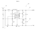
Fig. 4 is a circuit diagram illustrating an exemplary embodiment of the DC-DC converter. - As illustrated in
Fig. 4 , the DC-DC converter 120 includes aboost converter 121, aninverter 122, and a switchingcontroller 123. The DC-DC converter 120 may also include only one of theboost converter 121 and theinverter 122 depending on the voltage levels to be generated from an input voltage. Apower supplier 110 provides a DC power supply to the DC-DC converter 120. A reference symbol (ELVDD) denotes a positive power voltage, and a reference symbol (ELVSS) denotes a negative power voltage. - The
boost converter 121 includes a first inductor L11 electrically coupled to thepower supplier 110, a first switch M11 electrically coupled to the first inductor L11, a second switch M12 electrically coupled to the first inductor L11 and the first switch M11, first and second resistors R11 and R12 electrically coupled to the second switch M12, and a first capacitor C11 electrically coupled to the second switch M12. - Here, the first switch M11 may be an N-channel field-effect transistor and the second switch M12 may be a P-channel field-effect transistor but the invention is not limited thereto. For example, the first switch M11 may be a P-channel field-effect transistor and the second switch M12 may be an N-channel field-effect transistor. The voltage conversion is most efficient when the second switch M12 is turned off when the first switch M11 is turned on and when the first switch M11 is turned off when the second switch M12 is turned on. Furthermore, stress on the second switch M12 caused by the free-wheeling voltage produced by the current through the inductor L11 being shut off is reduced.
- The
inverter 122 includes a third switch M21 electrically coupled to thepower supplier 110, a second inductor L21 electrically coupled between the first switch M11 and the third switch M21, a fourth switch M22 electrically coupled between the third switch M21 and the second inductor L21, third and fourth resistors R21 and R22 electrically coupled to the fourth switch M22, and a second capacitor C21 electrically coupled to the fourth switch M22. - In the present embodiment, the third switch M21 is a P-channel field-effect transistor and the fourth switch M22 is an N-channel field-effect transistor, but the invention is not limited thereto. For example, the third switch M21 may be an N-channel field-effect transistor and the fourth switch M22 may be a P-channel field-effect transistor. As before, the voltage conversion is most efficient when the third switch M21 is turned on when the fourth switch M22 is turned off and when the third switch M21 is turned off when the fourth switch M22 is turned on. Furthermore, stress on the fourth switch M22 caused by the free-wheeling voltage produced by the current through the inductor L21 being shut off is reduced.
- In addition, when the first switch M11 of the
boost converter 121 is turned on, the third switch M21 of theinverter 122 is turned off and when the first switch M11 of theboost converter 121 is turned off, the third switch M21 of theinverter 122 is turned on. However, it is also possible that theboost converter 121 and theinverter 122 operate independently from each other. - The switching
controller 123 controls the first switch M11 and the second switch M12 of theboost converter 121. Further, the switchingcontroller 123 controls the third switch M21 and the fourth switch M22 of theinverter 122. In addition, an enable terminal (Ena) is electrically coupled to the switchingcontroller 123. An enable signal is input to the enable terminal (Ena) to operate the switchingcontroller 123 or a disable signal is input to the enable terminal Ena to stop the operation of the switchingcontroller 123. - In one embodiment, the first switch M11 and the second switch M12 of the
boost converter 121 and the third switch M21 and the fourth switch M22 of theinverter 122 may be integrated with the switchingcontroller 123. That is, even though the first to fourth switches M11 to M22 are illustrated outside the switching converter inFig. 4 , the first to fourth switches M11 to M22 may be substantially integrated inside the switchingcontroller 123. Therefore, according to the present embodiment of the invention, the size and weight of the overall DC-DC converter 120 may be considerably reduced. - In addition, a positive power voltage (ELVDD) is output through the
boost converter 121 and a negative power voltage (ELVSS) is output through theinverter 122. The positive power voltage (ELVDD) and the negative power voltage (ELVSS) are supplied to the above-described organic light emitting display panel. -
Fig. 5 is a block diagram illustrating the structure of a switching controller of an embodiment of the DC-DC converter. - As illustrated in
Fig. 5 , the switchingcontroller 123 includes afirst comparator 123a, asecond comparator 123b, acontrol logic unit 123c, afirst driver 123d, and asecond driver 123e. - An enable terminal (Ena) is electrically coupled to the
control logic unit 123c so as to input an enable signal or a disable signal from outside. - The
first comparator 123a is electrically coupled to a node between the first resistor R11 and the second resistor R12 of theboost converter 121. Therefore, a voltage divided by the first resistor R11 and the second resistor R12 is applied to thefirst comparator 123a. Accordingly, thefirst comparator 123a outputs a control signal to thecontrol logic unit 123c so as to keep a first positive power voltage (ELVDD) to be substantially constant. Therefore, thecontrol logic unit 123c outputs a control signal, which may be predetermined, to be electrically coupled to thefirst driver 123d. Further, switching frequencies of the first and second switches M11 and M12, which may be integrated with the switchingcontroller 123 appropriately change, thereby enabling the substantially constant positive power voltage (ELVDD). - The
second comparator 123b is electrically coupled to a node between the third resistor R21 and the fourth resistor R22 of theinverter 122. Therefore, a voltage divided by the third resistor R21 and the fourth resistor R22 is applied to thesecond comparator 123b. Accordingly, thesecond comparator 123b outputs a control signal to thecontrol logic unit 123c so as to keep a negative power voltage (ELVSS) to be substantially constant. Therefore, thecontrol logic unit 123c outputs a control signal, which may be predetermined, to be electrically coupled to thesecond driver 123e. Further, switching frequencies of the third and fourth switches M21 and M22, which may be integrated with the switchingcontroller 123 appropriately change, thereby enabling the substantially constant negative power voltage (ELVSS). - Further, according to an embodiment of the present invention, when the enable signal is input through the enable terminal (Ena), the
control logic unit 123c outputs control signals including an operation command to thefirst driver 123d and thesecond driver 123e so as to operate the first switch M11, the second switch M12, the third switch M21, and the fourth switch M22. However, when the disable signal is input through the enable terminal (Ena), thecontrol logic unit 123c outputs control signals including an operation stop command to thefirst driver 123d and thesecond driver 123e so as not to operate the first switch M11, the second switch M12, the third switch M21, and the fourth switch M22. In particular, because the second switch M12 and the fourth switch M22 are turned off, the power supply is not provided to the organic light emitting display panel. That is, the DC-DC converter is truly shut off. -
Fig. 6 is a graph illustrating the states in which the first switch and the second switch of the boost converter and the third switch and the fourth switch of the inverter included in the DC-DC converter are turned on. - As illustrated in
Fig. 6 , in the DC-DC converter, when the first switch M11 of the boost converter is turned on, the second switch M12 is turned off. Meanwhile, when the first switch M11 is turned off, the second switch M12 is turned on. - Further, when the third switch M21 of the inverter is turned on, the fourth switch M22 is turned off and when the third switch M21 is turned off, the fourth switch M22 is turned on.
- On the other hand, as illustrated in
Fig. 6 , in the DC-DC converter, when the first switch M11 of the boost converter is turned on, the third switch M21 of theinverter 122 is turned off and when the first switch M11 of the boost converter is turned off, the third switch M21 of theinverter 122 is turned on. As mentioned before, it is also possible that theboost converter 121 and theinverter 122 operate independently from each other. -
Figs. 7a to 7d are circuit diagrams illustrating the operation of the DC-DC converter. - In practice, the
boost converter 121 and theinverter 122 operate concurrently. However, for the convenience of the description, the operation of theboost converter 121 will be described separately from the operation of theinverter 122. - First, as illustrated in
Fig. 7a , the switchingcontroller 123 provides a signal at a high level to the first switch M11 and the second switch M12 of theboost converter 121. This way, the first switch M11 of theboost converter 121 is turned on and the second switch M12 of theboost converter 121 is turned off. - Therefore, a circuit loop through the first inductor L11 and the first switch M11 of the
boost converter 121 is closed, as illustrated by the arrow inFig.7a . Accordingly, the power supply provided from thepower supplier 110 is induced to the first inductor L11. That is, energy provided from thepower supplier 110 is stored in the first inductor L11. At this time, the switchingcontroller 123 adjusts a duty cycle with respect to the first switch M11 of theboost converter 121 so as to adjust the voltage drop across the first inductor L11. That is, a level of a voltage to be induced across the first inductor L11 varies depending on a period of time at which the first switch M11 is turned on. - Next, as illustrated in
Fig. 7b , the switchingcontroller 123 provides a signal at a low level to the first switch M11 and the second switch M12 of theboost converter 121. This way, the first switch M11 of theboost converter 121 is turned off and the second switch M12 of theboost converter 121 is turned on. - Therefore, the input voltage modified by the voltage drop across the first inductor L11 of the
boost converter 121 is applied to the first capacitor C11 through the second switch M12. That is, the positive power voltage is charged in the first capacitor C11. Furthermore, the second switch M12 and the first capacitor C11 output a positive power voltage (ELVDD) to the organic light emitting display panel. - Turning now to the operation of the
inverter 122, as illustrated inFig. 7c , the switchingcontroller 123 provides a signal at a low level to the third switch M21 and the fourth switch M22 of theinverter 122. This way, the third switch M21 of theinverter 122 is turned on and the fourth switch M22 of theinverter 122 is turned off. - Therefore, a circuit loop through the third switch M21 and the second inductor L21 of the
inverter 122 is closed, as illustrated by the arrow inFig. 7c . Accordingly, the power supply provided from thepower supplier 110 is induced to the second inductor L21. That is, energy provided from thepower supplier 110 is stored in the second inductor L21. At this time, the switchingcontroller 123 adjusts a duty cycle with respect to the third switch M21 of theinverter 122 so as to adjust the voltage drop across the second inductor L21. That is, a level of a voltage to be induced across the second inductor L21 varies depending on a period of time at which the third switch M21 is turned on. - As illustrated in
Fig. 7d , the switchingcontroller 123 provides a signal at a high level to the third switch M21 and the fourth switch M22 of theinverter 122. This way, the third switch M21 of theinverter 122 is turned off and the fourth switch M22 of theinverter 122 is turned on. - Therefore, as a current through the second inductor L21 decreases, a voltage across the second inductor L21 of the
inverter 122 is inverted and applied to the second capacitor C21 through the fourth switch M22. That is, the voltage across the second inductor L21 is inverted and charged in the second capacitor C21. Furthermore, the fourth switch M22 and the second capacitor C21 output a negative power voltage (ELVSS) to the organic light emitting display panel. -
Fig. 8 is a circuit diagram illustrating another operation of the DC-DC converter. - As illustrated in
Fig. 8 , a disable signal may be input to the enable terminal Ena, which is electrically coupled to the switchingcontroller 123. For example, in order to completely stop the operation of the organiclight emitting display 100, a disable signal may be input to the enable terminal (Ena). Thereafter, the switchingcontroller 123 outputs a signal at a high level to the second switch M12 of theboost converter 121 and outputs a signal at a low level to the fourth switch M22 of theinverter 122. Accordingly, the second switch M12 of theboost converter 121 and the fourth switch M22 of theinverter 122 are turned off. - Therefore, the power supply provided from the
power supplier 110 is not provided to the organic light emitting display panel through the second switch M12 and the fourth switch M22. In other words, the DC-DC converter is truly shut down. Accordingly, it is possible to reduce the overall power consumption of the organic light emitting display and to decrease the deterioration of the organic light emitting display. -
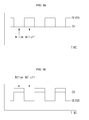
Figs. 9a to 9b are graphs illustrating waveforms of a positive power voltage and a negative power voltage output from the DC-DC converter. Here,Fig. 9a shows a waveform of the voltage input to the second switch M12 when no first capacitor C11 is present, andFig. 9b shows a waveform of the voltage input to the fourth switch M22 when no second capacitor C21 is present. When smoothing is performed by the first and second capacitors C11, C21, the positive power voltage (ELVDD) to be applied to the organic light emitting display panel is an approximately smooth direct current voltage because the voltage supplied during the "M11 off'-phases is stored in the first capacitor C11 such that the output voltage of theboost converter 121 rises to the desired value ELVDD and the negative power voltage (ELVSS) is an approximately smooth direct current voltage because the voltage supplied during the "M21-off"-phases is stored in the second capacitor C21 such that the output voltage of theinverter 122 sinks to the desired value ELVSS. - First, as illustrated in
Fig. 9a , when the first switch M11 of theboost converter 121 is turned off, the positive power voltage (ELVDD) stored in the first inductor L11 is output. Here, the positive power voltage (ELVDD) may be obtained by using the followingEquation 1.
- Here, reference symbol Vin denotes an input voltage applied from the
power supplier 110 and reference symbol D denotes the duty cycle. - Next, as illustrated in
Fig. 9b , when the third switch M21 of theinverter 122 is turned off, the negative power voltage (ELVSS) stored in the second inductor L21 is output. Here, the negative power voltage (ELVSS) may be obtained by using following Equation 2.
- As described above, the negative power voltage (ELVSS) is determined by using Equation 2. In particular, in the range of D > 0.5, the absolute value of the negative power voltage (ELVSS) is larger than the input voltage Vin and in the range of D < 0.5, the absolute value of the negative power voltage (ELVSS) is smaller than the input voltage Vin. In an exemplary embodiment according to the invention, the P-channel transistor is adopted in the
inverter 122 and the duty cycle is controlled to be larger than 0.5. Therefore, the negative power voltage (ELVSS) having an absolute value larger than the input value is output. In other words, if it is assumed that a desired negative power voltage (ELVSS) is approximately -6V, theinverter 122 raises an input voltage from approximately 3V to 6V, inverts the input voltage into the negative power voltage (ELVSS), and outputs the inverted voltage. - Therefore, according to this embodiment of the invention, the freewheel diode from a conventional DC-DC converter may be replaced with a switch having a low voltage drop. Therefore, it is possible to provide a DC-DC converter having lower power consumption.
- Further, according to an embodiment of the invention, it is possible to supply a light-weight and small size DC-DC converter by integrating the freewheel diode with a switching controller while replacing the freewheel diode with the switch.
- Further, according to an embodiment of the invention, it is possible to supply a DC-DC converter which is truly shut down by using a switch in a boost converter and a switch in an inverter, which function as the freewheel diode, to be turned off when the switching controller does not operate.
Claims (9)
- A DC-DC converter (120) for an organic light emitting display, having a first voltage converter (121, 122) comprising:a first inductor (L11, L21) and a first switch (M11, M21) series-connected between a first power supply voltage input and a second power supply voltage input;a second switch (M12, M22) having a first electrode connected to a first common node between the first inductor (L11, L21) and the first switch (M11, M21) and a second electrode connected to a first output terminal (ELVDD, ELVSS); anda switching controller (123) having an enable input (Ena), a first control output connected to a control electrode of the first switch (M11, M21), and a second control output connected to a control electrode of the second switch (M12, M22),wherein the switching controller (123) is adapted to provide first and second control signals to the first switch (M11, M21) and the second switch (M12, M22), respectively, in response to an enable signal received at the enable input (Ena) to thereby control an on-time and an off-time of the first switch (M11, M21) and the second switch (M12, M22).
- The DC-DC converter (120) of claim 1, wherein the first voltage converter (121, 122) further comprises a first voltage divider (R11, R12; R21, R22) connected between the first output terminal (ELVDD, ELVSS) and a first reference voltage input and adapted to provide a feedback voltage to a control input of the switching controller (123).
- The DC-DC converter (120) of one of claims 1 or 2, wherein the first voltage converter (121, 122) further comprises a first capacitor (C11, C21) having a first terminal connected to the first output terminal (ELVDD, ELVSS) and a second terminal connected to the second power supply voltage input.
- The DC-DC converter (120) of one of the preceding claims, wherein the first inductor (L11) has a first terminal connected to the first power supply voltage input and wherein the first switch (M11) has one of a first and a second electrode connected to the second power supply voltage input.
- The DC-DC converter (120) of one of the claims 1 through 3, wherein the first inductor (L21) has a first terminal connected to the second power supply voltage input and wherein the first switch (M21) has one of a first and a second electrode connected to the first power supply voltage input.
- The DC-DC converter (120) of one of the preceding claims, wherein the first switch (M11, M21) is of a different polarity type than the second switch (M12, M22).
- The DC-DC converter (120) of one of the preceding claims, further comprising a second voltage converter (121, 122) comprising:a second inductor (L11, L21) and a third switch (M11, M21) series-connected between the first power supply voltage input and the second power supply voltage input;a fourth switch (M12, M22) having a first electrode connected to a second common node between the second inductor (L11, L21) and the third switch (M11, M21) and a second electrode connected to a second output terminal (ELVDD, ELVSS),wherein a third control output of the switching controller (123) is connected to a control electrode of the third switch (M11, M21), and a fourth control output of the switching controller (123) is connected to a control electrode of the fourth switch (M12, M22),
wherein the switching controller (123) is adapted to provide third and fourth control signals to the third switch (M11, M21) and the fourth switch (M12, M22), respectively, in response to the enable signal received at the enable input (Ena) to thereby control an on-time and an off-time of the third switch (M11, M21) and the fourth switch (M12, M22), and
wherein, if the first inductor (L11, L21) has one terminal connected to the first power supply voltage input, the second inductor (L11, L21) has one terminal connected to the second power supply voltage input, and wherein the second inductor (L11, L21) has one terminal connected to the first power supply voltage input else. - The DC-DC converter (120) of claims 6 and 7, wherein the third switch (M11, M21) is of the same polarity type as the second switch (M12, M22) and wherein the fourth switch (M12, M22) is of the same polarity type as the first switch (M11, M21).
- An organic light emitting display having a power supplier, a DC-DC converter, a scan driver, a data driver, and an organic light emitting display panel, characterised in that the DC-DC converter is a DC-DC converter according to one of the preceding claims.
Applications Claiming Priority (1)
| Application Number | Priority Date | Filing Date | Title |
|---|---|---|---|
| KR1020070006545A KR100833764B1 (en) | 2007-01-22 | 2007-01-22 | Organic light emitting display having dc-dc converter |
Publications (2)
| Publication Number | Publication Date |
|---|---|
| EP1951005A1 true EP1951005A1 (en) | 2008-07-30 |
| EP1951005B1 EP1951005B1 (en) | 2014-03-12 |
Family
ID=39301069
Family Applications (1)
| Application Number | Title | Priority Date | Filing Date |
|---|---|---|---|
| EP08150486.2A Active EP1951005B1 (en) | 2007-01-22 | 2008-01-22 | Organic light emitting display having DC-DC converter |
Country Status (6)
| Country | Link |
|---|---|
| US (1) | US8334824B2 (en) |
| EP (1) | EP1951005B1 (en) |
| JP (1) | JP5323345B2 (en) |
| KR (1) | KR100833764B1 (en) |
| CN (1) | CN101231818B (en) |
| TW (1) | TWI369664B (en) |
Cited By (12)
| Publication number | Priority date | Publication date | Assignee | Title |
|---|---|---|---|---|
| EP2151912A1 (en) * | 2008-08-06 | 2010-02-10 | Samsung Mobile Display Co., Ltd. | DC-DC converter and organic light emitting display device using the same |
| EP2237252A1 (en) | 2009-02-27 | 2010-10-06 | Samsung Mobile Display Co., Ltd. | DC-DC converter and organic light emitting display using the same |
| FR2954018A1 (en) * | 2009-12-16 | 2011-06-17 | St Microelectronics Tours Sas | MULTINIVEAL CUTTING FEEDING |
| EP2398012A1 (en) * | 2010-06-21 | 2011-12-21 | Samsung Mobile Display Co., Ltd. | Organic light emitting display and power supply for the same |
| GB2486822A (en) * | 2010-12-23 | 2012-06-27 | Lg Display Co Ltd | An OLED display with reduced leakage current in sleep mode |
| EP2637291A1 (en) * | 2012-03-06 | 2013-09-11 | Samsung Display Co., Ltd. | DC-DC converter and organic light-emitting display including the same |
| KR20130102256A (en) * | 2012-03-07 | 2013-09-17 | 삼성디스플레이 주식회사 | Power supply unit and organic light emitting display including the same |
| KR20130116411A (en) * | 2012-03-14 | 2013-10-24 | 삼성디스플레이 주식회사 | Dc-dc converter and organic light emitting display including the same |
| EP2568565A3 (en) * | 2011-09-06 | 2016-06-22 | Lg Electronics Inc. | Mobile terminal and power management unit thereof |
| KR20180112742A (en) * | 2018-09-21 | 2018-10-12 | 삼성디스플레이 주식회사 | DC-DC Converter and Organic Light Emitting Display including The Same |
| WO2020108759A1 (en) * | 2018-11-29 | 2020-06-04 | Siemens Aktiengesellschaft | Micro solar inverter |
| EP3631963A4 (en) * | 2017-05-31 | 2020-12-16 | Intuitive Surgical Operations Inc. | Electrosurgical output stage with integrated dc regulator |
Families Citing this family (42)
| Publication number | Priority date | Publication date | Assignee | Title |
|---|---|---|---|---|
| KR20090093019A (en) * | 2008-02-28 | 2009-09-02 | 삼성모바일디스플레이주식회사 | Dc-dc converter and organic light emitting display thereof |
| KR101022106B1 (en) * | 2008-08-06 | 2011-03-17 | 삼성모바일디스플레이주식회사 | Organic ligth emitting display |
| TWI407408B (en) * | 2008-09-04 | 2013-09-01 | Innolux Corp | Pixel unit, display panel and electric system utilizing the same |
| CN101673503A (en) * | 2008-09-12 | 2010-03-17 | 统宝光电股份有限公司 | Pixel unit and electronic system having the same |
| KR101325979B1 (en) * | 2008-12-24 | 2013-11-07 | 엘지디스플레이 주식회사 | Power supply unit for organic electroluminescent display device |
| KR101056331B1 (en) * | 2009-02-27 | 2011-08-11 | 삼성모바일디스플레이주식회사 | Power supply unit, organic light emitting display device using same and driving method thereof |
| KR101022085B1 (en) | 2009-07-10 | 2011-03-17 | 삼성모바일디스플레이주식회사 | Power supply and organic light emitting display device using the same |
| KR101064462B1 (en) | 2009-11-17 | 2011-09-15 | 삼성모바일디스플레이주식회사 | Dc-dc converter and organic light emitting display device for the same |
| KR101040798B1 (en) * | 2009-11-17 | 2011-06-14 | 삼성모바일디스플레이주식회사 | Dc-dc conveter and organic light emitting display device using the same |
| KR101023576B1 (en) | 2010-01-18 | 2011-03-21 | 청주대학교 산학협력단 | High efficiency switching power supplies and high efficiency soft switching half-bridge dc-dc converter thereof |
| KR101156446B1 (en) * | 2010-06-04 | 2012-06-18 | 삼성모바일디스플레이주식회사 | Organic electro luminescence Display and driving method thereof |
| KR20120013777A (en) * | 2010-08-06 | 2012-02-15 | 삼성모바일디스플레이주식회사 | Organic light emitting display apparatus and method of providing power thereof |
| KR101323390B1 (en) * | 2010-09-20 | 2013-10-29 | 엘지디스플레이 주식회사 | Organic light emitting diode display device and low power driving method thereof |
| KR101886743B1 (en) * | 2010-12-20 | 2018-08-10 | 삼성디스플레이 주식회사 | Pulse Generator and Organic Light Emitting Display Device Using the same |
| KR101788218B1 (en) | 2011-01-06 | 2017-10-20 | 삼성디스플레이 주식회사 | DC-DC Converter and Mobile Communication Terminal using The Same |
| KR101816256B1 (en) | 2011-04-08 | 2018-01-09 | 삼성디스플레이 주식회사 | Organic Light Emitting Display having a Short Detection Circuit and Driving Method Thereof |
| KR101860739B1 (en) | 2011-05-18 | 2018-05-25 | 삼성디스플레이 주식회사 | Supply voltage converter, display device including the same and method of controlling driving voltage |
| KR101871906B1 (en) * | 2011-06-30 | 2018-06-28 | 삼성디스플레이 주식회사 | DC-DC Converter and Organic Light Emitting Display including The Same |
| KR101476880B1 (en) * | 2011-09-29 | 2014-12-29 | 엘지디스플레이 주식회사 | Organic light emitting diode display device |
| KR101305869B1 (en) * | 2011-10-12 | 2013-09-09 | 포항공과대학교 산학협력단 | Simplified organic emitting diode and method for preparing the same |
| US20130169610A1 (en) * | 2011-12-30 | 2013-07-04 | Stmicroelectronics (Shenzhen) R&D Co. Ltd. | Driving circuit and display device |
| KR101965892B1 (en) * | 2012-03-05 | 2019-04-08 | 삼성디스플레이 주식회사 | DC-DC Converter and Organic Light Emitting Display Device Using the same |
| KR101992281B1 (en) * | 2012-03-06 | 2019-06-26 | 삼성디스플레이 주식회사 | Organic Light Emitting Display and Driving Method Thereof |
| KR20140000075A (en) * | 2012-06-22 | 2014-01-02 | 삼성디스플레이 주식회사 | Power unit and organic light emitting display device having the same |
| DE102012218543A1 (en) | 2012-10-11 | 2014-04-17 | Continental Automotive Gmbh | Device for voltage conversion and electrical system with a device mentioned |
| KR20140054760A (en) * | 2012-10-29 | 2014-05-09 | 삼성디스플레이 주식회사 | Organic light emitting display |
| US9535440B2 (en) * | 2012-10-30 | 2017-01-03 | Samsung Display Co., Ltd. | DC-DC converter and organic light emitting display device using the same |
| KR20140055068A (en) * | 2012-10-30 | 2014-05-09 | 삼성디스플레이 주식회사 | Dc-dc converter and organic light emitting display device using the same |
| US9337731B2 (en) * | 2012-12-13 | 2016-05-10 | Linear Technology Corporation | Power converter for generating both positive and negative output signals |
| KR102057286B1 (en) | 2013-02-21 | 2019-12-19 | 삼성디스플레이 주식회사 | Organic Light Emitting Display |
| KR102071004B1 (en) * | 2013-09-03 | 2020-01-30 | 삼성디스플레이 주식회사 | Dc-dc converter and organic light emitting display including the same |
| DE102014203157A1 (en) * | 2014-02-21 | 2015-08-27 | Airbus Operations Gmbh | Bipolar high voltage network and method for operating a bipolar high voltage network |
| CN104868720B (en) * | 2014-02-26 | 2017-11-14 | 万国半导体股份有限公司 | The power driving circuit of oled panel and the method for driving load |
| KR20160008033A (en) * | 2014-07-11 | 2016-01-21 | 삼성디스플레이 주식회사 | Dc-dc converter and organic light emittng display device including the same |
| CN105281377B (en) * | 2014-07-16 | 2018-08-28 | 立锜科技股份有限公司 | Input/output signal processing circuit and input/output signal processing method |
| CN104157239A (en) * | 2014-07-21 | 2014-11-19 | 京东方科技集团股份有限公司 | Pixel circuit, driving method of pixel circuit, and display device adopting pixel circuit |
| KR102504645B1 (en) | 2016-02-23 | 2023-03-02 | 삼성디스플레이 주식회사 | Boost convertor, display device including the same, and method of controlling power |
| CN106448561B (en) * | 2016-10-21 | 2017-11-10 | 京东方科技集团股份有限公司 | For the device and method for the EL driving voltages for controlling display panel |
| DE102017212462A1 (en) * | 2017-07-20 | 2019-01-24 | Siemens Aktiengesellschaft | Galvanically coupled electrical converter |
| KR102610428B1 (en) * | 2018-11-05 | 2023-12-07 | 삼성디스플레이 주식회사 | Dc-dc converter, display device having the same, and driving method thereof |
| CN209103800U (en) * | 2018-11-29 | 2019-07-12 | 惠科股份有限公司 | Display panel, drive circuit |
| KR102148498B1 (en) * | 2020-03-26 | 2020-08-27 | 삼성디스플레이 주식회사 | Dc-dc converter and organic light emitting display device using the same |
Citations (5)
| Publication number | Priority date | Publication date | Assignee | Title |
|---|---|---|---|---|
| US4736151A (en) * | 1986-12-23 | 1988-04-05 | Sundstrand Corporation | Bi-directional buck/boost DC/DC converter |
| US5412308A (en) * | 1994-01-06 | 1995-05-02 | Hewlett-Packard Corporation | Dual voltage power supply |
| US20030090245A1 (en) * | 2001-11-05 | 2003-05-15 | Krishna Shenai | Synchronous switched boost and buck converter |
| EP1365632A1 (en) * | 2002-05-21 | 2003-11-26 | Wintest Corporation | Inspection method and device for active matrix |
| US20060097707A1 (en) * | 2004-11-05 | 2006-05-11 | Denso Corporation | Power control circuit for charge storage element |
Family Cites Families (21)
| Publication number | Priority date | Publication date | Assignee | Title |
|---|---|---|---|---|
| JPS50156654A (en) * | 1974-06-10 | 1975-12-18 | ||
| JPH0710166B2 (en) * | 1985-05-21 | 1995-02-01 | ソニー株式会社 | Switching Regulator |
| US5481178A (en) * | 1993-03-23 | 1996-01-02 | Linear Technology Corporation | Control circuit and method for maintaining high efficiency over broad current ranges in a switching regulator circuit |
| JPH07213049A (en) * | 1994-01-14 | 1995-08-11 | Toko Inc | Switching power unit |
| JPH08242577A (en) * | 1995-03-02 | 1996-09-17 | Sony Corp | Switching regulator |
| JP2001178121A (en) * | 1999-12-14 | 2001-06-29 | Taiyo Yuden Co Ltd | Electronic component |
| TWI238375B (en) * | 2000-05-31 | 2005-08-21 | Toshiba Corp | Pumping circuit and flat panel display device |
| TWI221595B (en) | 2000-09-29 | 2004-10-01 | Sanyo Electric Co | Driving apparatus for display device |
| US6525488B2 (en) * | 2001-05-18 | 2003-02-25 | General Electric Company | Self-oscillating synchronous boost converter |
| KR100878222B1 (en) * | 2001-07-03 | 2009-01-13 | 삼성전자주식회사 | Apparatus for supplying power for a liquid crystal display |
| US6946820B2 (en) * | 2001-09-12 | 2005-09-20 | Matsushita Electric Industrial Co., Ltd. | Multiple output DC-DC converter for providing controlled voltages |
| TW563088B (en) * | 2001-09-17 | 2003-11-21 | Semiconductor Energy Lab | Light emitting device, method of driving a light emitting device, and electronic equipment |
| US6643158B2 (en) * | 2001-10-31 | 2003-11-04 | Mobility Electronics, Inc. | Dual input AC/DC to programmable DC output converter |
| US7190151B2 (en) * | 2003-03-18 | 2007-03-13 | International Rectifier Corporation | High intensity discharge lamp ballast circuit |
| CN1868107A (en) | 2003-10-13 | 2006-11-22 | 皇家飞利浦电子股份有限公司 | Boost converter |
| JP4803629B2 (en) * | 2004-04-27 | 2011-10-26 | 東北パイオニア株式会社 | Light emitting display device and drive control method thereof |
| KR100604058B1 (en) | 2004-09-24 | 2006-07-24 | 삼성에스디아이 주식회사 | DC/DC Converter in Light Emitting Display and Driving Method Using The Same |
| JP4599146B2 (en) * | 2004-11-30 | 2010-12-15 | 株式会社アドバンテスト | Test device and power supply circuit |
| JP2006276713A (en) * | 2005-03-30 | 2006-10-12 | Toshiba Matsushita Display Technology Co Ltd | Power supply circuit for el display apparatus |
| US7948455B2 (en) * | 2005-10-20 | 2011-05-24 | 02Micro Inc. | Apparatus and method for regulating white LEDs |
| US7667414B2 (en) * | 2006-05-24 | 2010-02-23 | Stanley Electric Co., Ltd. | LED lighting apparatus |
-
2007
- 2007-01-22 KR KR1020070006545A patent/KR100833764B1/en active IP Right Grant
- 2007-12-17 JP JP2007324753A patent/JP5323345B2/en active Active
- 2007-12-28 US US11/966,797 patent/US8334824B2/en active Active
- 2007-12-31 TW TW096151498A patent/TWI369664B/en active
-
2008
- 2008-01-10 CN CN2008100026237A patent/CN101231818B/en active Active
- 2008-01-22 EP EP08150486.2A patent/EP1951005B1/en active Active
Patent Citations (5)
| Publication number | Priority date | Publication date | Assignee | Title |
|---|---|---|---|---|
| US4736151A (en) * | 1986-12-23 | 1988-04-05 | Sundstrand Corporation | Bi-directional buck/boost DC/DC converter |
| US5412308A (en) * | 1994-01-06 | 1995-05-02 | Hewlett-Packard Corporation | Dual voltage power supply |
| US20030090245A1 (en) * | 2001-11-05 | 2003-05-15 | Krishna Shenai | Synchronous switched boost and buck converter |
| EP1365632A1 (en) * | 2002-05-21 | 2003-11-26 | Wintest Corporation | Inspection method and device for active matrix |
| US20060097707A1 (en) * | 2004-11-05 | 2006-05-11 | Denso Corporation | Power control circuit for charge storage element |
Cited By (21)
| Publication number | Priority date | Publication date | Assignee | Title |
|---|---|---|---|---|
| EP2151912A1 (en) * | 2008-08-06 | 2010-02-10 | Samsung Mobile Display Co., Ltd. | DC-DC converter and organic light emitting display device using the same |
| US8803769B2 (en) | 2009-02-27 | 2014-08-12 | Samsung Display Co., Ltd. | DC-DC converter and organic light emitting display using the same |
| EP2237252A1 (en) | 2009-02-27 | 2010-10-06 | Samsung Mobile Display Co., Ltd. | DC-DC converter and organic light emitting display using the same |
| FR2954018A1 (en) * | 2009-12-16 | 2011-06-17 | St Microelectronics Tours Sas | MULTINIVEAL CUTTING FEEDING |
| EP2337205A1 (en) * | 2009-12-16 | 2011-06-22 | STMicroelectronics (Tours) SAS | Multi-level switching-mode power supply |
| EP2398012A1 (en) * | 2010-06-21 | 2011-12-21 | Samsung Mobile Display Co., Ltd. | Organic light emitting display and power supply for the same |
| US9165498B2 (en) | 2010-06-21 | 2015-10-20 | Samsung Display Co., Ltd. | Organic light emitting display and power supply for the same |
| GB2486822A (en) * | 2010-12-23 | 2012-06-27 | Lg Display Co Ltd | An OLED display with reduced leakage current in sleep mode |
| US8842110B2 (en) | 2010-12-23 | 2014-09-23 | Lg Display Co., Ltd. | Organic light emitting diode display and driving method thereof |
| GB2486822B (en) * | 2010-12-23 | 2012-12-19 | Lg Display Co Ltd | Organic light emitting diode display and driving method thereof |
| EP2568565A3 (en) * | 2011-09-06 | 2016-06-22 | Lg Electronics Inc. | Mobile terminal and power management unit thereof |
| EP2637291A1 (en) * | 2012-03-06 | 2013-09-11 | Samsung Display Co., Ltd. | DC-DC converter and organic light-emitting display including the same |
| US9337718B2 (en) | 2012-03-06 | 2016-05-10 | Samsung Display Co., Ltd. | DC-DC converter and organic light emitting display including the same |
| US9875692B2 (en) | 2012-03-06 | 2018-01-23 | Samsung Display Co., Ltd. | DC-DC converter and organic light emitting display including the same |
| KR20130102256A (en) * | 2012-03-07 | 2013-09-17 | 삼성디스플레이 주식회사 | Power supply unit and organic light emitting display including the same |
| KR20130116411A (en) * | 2012-03-14 | 2013-10-24 | 삼성디스플레이 주식회사 | Dc-dc converter and organic light emitting display including the same |
| EP3631963A4 (en) * | 2017-05-31 | 2020-12-16 | Intuitive Surgical Operations Inc. | Electrosurgical output stage with integrated dc regulator |
| US11701163B2 (en) | 2017-05-31 | 2023-07-18 | Intuitive Surgical Operations, Inc. | Electrosurgical output stage with integrated DC regulator |
| KR20180112742A (en) * | 2018-09-21 | 2018-10-12 | 삼성디스플레이 주식회사 | DC-DC Converter and Organic Light Emitting Display including The Same |
| WO2020108759A1 (en) * | 2018-11-29 | 2020-06-04 | Siemens Aktiengesellschaft | Micro solar inverter |
| AU2018451265B2 (en) * | 2018-11-29 | 2022-06-30 | Siemens Aktiengesellschaft | Micro solar inverter |
Also Published As
| Publication number | Publication date |
|---|---|
| CN101231818A (en) | 2008-07-30 |
| TWI369664B (en) | 2012-08-01 |
| KR100833764B1 (en) | 2008-05-29 |
| TW200844950A (en) | 2008-11-16 |
| EP1951005B1 (en) | 2014-03-12 |
| CN101231818B (en) | 2010-06-09 |
| JP5323345B2 (en) | 2013-10-23 |
| US8334824B2 (en) | 2012-12-18 |
| US20080174287A1 (en) | 2008-07-24 |
| JP2008176306A (en) | 2008-07-31 |
Similar Documents
| Publication | Publication Date | Title |
|---|---|---|
| EP1951005B1 (en) | Organic light emitting display having DC-DC converter | |
| US10879802B2 (en) | DC-DC converter and display apparatus having the same | |
| US8803769B2 (en) | DC-DC converter and organic light emitting display using the same | |
| US7888920B2 (en) | Power supply device with fast output voltage switching capability | |
| US20070069712A1 (en) | Driving circuit and electronic device using the same | |
| WO2007010802A1 (en) | Step-up switching regulator and its control circuit and electronic apparatus employing it | |
| US8970575B2 (en) | Power source circuit and liquid crystal display apparatus having the same | |
| US7528589B2 (en) | Step-up DC/DC converter and electronic appliance therewith | |
| US20170243534A1 (en) | Power supply circuit, driving method for the same and display device | |
| TWI596877B (en) | Dc-dc converter and organic light emitting display device using the same | |
| US11870343B1 (en) | Switched capacitor recirculating converter circuits | |
| KR101554583B1 (en) | Organic electroluminescent display and method of driving the same | |
| KR20060112996A (en) | Light emitting display | |
| Ge et al. | On-chip boost DC-DC converter in color OLED driver & controller ICs for mobile application | |
| KR100859655B1 (en) | Organic light emitting desplay | |
| Wang et al. | Efficiency enhanced single-inductor boost-inverting flyback converter with dual hybrid energy transfer media and a bifurcation free comparator | |
| Ding et al. | A 96% Peak Efficiency Off-chip Capacitor Free Dimmable Hysteresis Current Control LED Driver | |
| CN219287374U (en) | Boost circuit and electronic equipment | |
| KR20220040571A (en) | Display device and method for operating display device | |
| JP2008048573A (en) | Power-supply device, and electronic equipment provided therewith |
Legal Events
| Date | Code | Title | Description |
|---|---|---|---|
| PUAI | Public reference made under article 153(3) epc to a published international application that has entered the european phase |
Free format text: ORIGINAL CODE: 0009012 |
|
| 17P | Request for examination filed |
Effective date: 20080123 |
|
| AK | Designated contracting states |
Kind code of ref document: A1 Designated state(s): AT BE BG CH CY CZ DE DK EE ES FI FR GB GR HR HU IE IS IT LI LT LU LV MC MT NL NO PL PT RO SE SI SK TR |
|
| AX | Request for extension of the european patent |
Extension state: AL BA MK RS |
|
| 17Q | First examination report despatched |
Effective date: 20081031 |
|
| RAP1 | Party data changed (applicant data changed or rights of an application transferred) |
Owner name: SAMSUNG MOBILE DISPLAY CO., LTD. |
|
| AKX | Designation fees paid |
Designated state(s): DE FR GB HU IT PL |
|
| RAP1 | Party data changed (applicant data changed or rights of an application transferred) |
Owner name: SAMSUNG DISPLAY CO., LTD. |
|
| GRAP | Despatch of communication of intention to grant a patent |
Free format text: ORIGINAL CODE: EPIDOSNIGR1 |
|
| INTG | Intention to grant announced |
Effective date: 20130926 |
|
| GRAS | Grant fee paid |
Free format text: ORIGINAL CODE: EPIDOSNIGR3 |
|
| GRAA | (expected) grant |
Free format text: ORIGINAL CODE: 0009210 |
|
| AK | Designated contracting states |
Kind code of ref document: B1 Designated state(s): DE FR GB HU IT PL |
|
| REG | Reference to a national code |
Ref country code: GB Ref legal event code: FG4D |
|
| REG | Reference to a national code |
Ref country code: DE Ref legal event code: R096 Ref document number: 602008030744 Country of ref document: DE Effective date: 20140424 |
|
| PG25 | Lapsed in a contracting state [announced via postgrant information from national office to epo] |
Ref country code: PL Free format text: LAPSE BECAUSE OF FAILURE TO SUBMIT A TRANSLATION OF THE DESCRIPTION OR TO PAY THE FEE WITHIN THE PRESCRIBED TIME-LIMIT Effective date: 20140312 |
|
| REG | Reference to a national code |
Ref country code: DE Ref legal event code: R097 Ref document number: 602008030744 Country of ref document: DE |
|
| PLBE | No opposition filed within time limit |
Free format text: ORIGINAL CODE: 0009261 |
|
| STAA | Information on the status of an ep patent application or granted ep patent |
Free format text: STATUS: NO OPPOSITION FILED WITHIN TIME LIMIT |
|
| 26N | No opposition filed |
Effective date: 20141215 |
|
| REG | Reference to a national code |
Ref country code: DE Ref legal event code: R097 Ref document number: 602008030744 Country of ref document: DE Effective date: 20141215 |
|
| PG25 | Lapsed in a contracting state [announced via postgrant information from national office to epo] |
Ref country code: IT Free format text: LAPSE BECAUSE OF FAILURE TO SUBMIT A TRANSLATION OF THE DESCRIPTION OR TO PAY THE FEE WITHIN THE PRESCRIBED TIME-LIMIT Effective date: 20140312 |
|
| REG | Reference to a national code |
Ref country code: FR Ref legal event code: PLFP Year of fee payment: 9 |
|
| REG | Reference to a national code |
Ref country code: FR Ref legal event code: PLFP Year of fee payment: 10 |
|
| PG25 | Lapsed in a contracting state [announced via postgrant information from national office to epo] |
Ref country code: HU Free format text: LAPSE BECAUSE OF FAILURE TO SUBMIT A TRANSLATION OF THE DESCRIPTION OR TO PAY THE FEE WITHIN THE PRESCRIBED TIME-LIMIT; INVALID AB INITIO Effective date: 20080122 |
|
| REG | Reference to a national code |
Ref country code: FR Ref legal event code: PLFP Year of fee payment: 11 |
|
| REG | Reference to a national code |
Ref country code: DE Ref legal event code: R079 Ref document number: 602008030744 Country of ref document: DE Free format text: PREVIOUS MAIN CLASS: H05B0033080000 Ipc: H05B0045000000 |
|
| P01 | Opt-out of the competence of the unified patent court (upc) registered |
Effective date: 20230515 |
|
| PGFP | Annual fee paid to national office [announced via postgrant information from national office to epo] |
Ref country code: GB Payment date: 20231220 Year of fee payment: 17 |
|
| PGFP | Annual fee paid to national office [announced via postgrant information from national office to epo] |
Ref country code: FR Payment date: 20231222 Year of fee payment: 17 |
|
| PGFP | Annual fee paid to national office [announced via postgrant information from national office to epo] |
Ref country code: DE Payment date: 20231220 Year of fee payment: 17 |