EP1852964A1 - Power conversion apparatus - Google Patents
Power conversion apparatus Download PDFInfo
- Publication number
- EP1852964A1 EP1852964A1 EP06714141A EP06714141A EP1852964A1 EP 1852964 A1 EP1852964 A1 EP 1852964A1 EP 06714141 A EP06714141 A EP 06714141A EP 06714141 A EP06714141 A EP 06714141A EP 1852964 A1 EP1852964 A1 EP 1852964A1
- Authority
- EP
- European Patent Office
- Prior art keywords
- power
- power source
- voltage
- inv
- maximum
- Prior art date
- Legal status (The legal status is an assumption and is not a legal conclusion. Google has not performed a legal analysis and makes no representation as to the accuracy of the status listed.)
- Granted
Links
Images


Classifications
-
- H—ELECTRICITY
- H02—GENERATION; CONVERSION OR DISTRIBUTION OF ELECTRIC POWER
- H02M—APPARATUS FOR CONVERSION BETWEEN AC AND AC, BETWEEN AC AND DC, OR BETWEEN DC AND DC, AND FOR USE WITH MAINS OR SIMILAR POWER SUPPLY SYSTEMS; CONVERSION OF DC OR AC INPUT POWER INTO SURGE OUTPUT POWER; CONTROL OR REGULATION THEREOF
- H02M7/00—Conversion of ac power input into dc power output; Conversion of dc power input into ac power output
- H02M7/42—Conversion of dc power input into ac power output without possibility of reversal
- H02M7/44—Conversion of dc power input into ac power output without possibility of reversal by static converters
- H02M7/48—Conversion of dc power input into ac power output without possibility of reversal by static converters using discharge tubes with control electrode or semiconductor devices with control electrode
- H02M7/53—Conversion of dc power input into ac power output without possibility of reversal by static converters using discharge tubes with control electrode or semiconductor devices with control electrode using devices of a triode or transistor type requiring continuous application of a control signal
- H02M7/537—Conversion of dc power input into ac power output without possibility of reversal by static converters using discharge tubes with control electrode or semiconductor devices with control electrode using devices of a triode or transistor type requiring continuous application of a control signal using semiconductor devices only, e.g. single switched pulse inverters
- H02M7/5387—Conversion of dc power input into ac power output without possibility of reversal by static converters using discharge tubes with control electrode or semiconductor devices with control electrode using devices of a triode or transistor type requiring continuous application of a control signal using semiconductor devices only, e.g. single switched pulse inverters in a bridge configuration
-
- H—ELECTRICITY
- H02—GENERATION; CONVERSION OR DISTRIBUTION OF ELECTRIC POWER
- H02M—APPARATUS FOR CONVERSION BETWEEN AC AND AC, BETWEEN AC AND DC, OR BETWEEN DC AND DC, AND FOR USE WITH MAINS OR SIMILAR POWER SUPPLY SYSTEMS; CONVERSION OF DC OR AC INPUT POWER INTO SURGE OUTPUT POWER; CONTROL OR REGULATION THEREOF
- H02M1/00—Details of apparatus for conversion
- H02M1/0067—Converter structures employing plural converter units, other than for parallel operation of the units on a single load
- H02M1/0077—Plural converter units whose outputs are connected in series
Abstract
Description
- The present invention relates to a power conversion apparatus that converts DC power to AC power, and particularly to a power conversion apparatus used for a power conditioner or the like that links a decentralized power source to a system.
- In a conventional power conditioner, for example, as seen in a solar power conditioner, the voltage from a decentralized power source that is a solar battery is boosted by using a chopper, and a PWM-controlled inverter is inserted onto the subsequent stage, thus generating an output AC voltage.
A basic operation of such a conventional power conditioner will be described hereinafter. DC power outputted from the solar battery drives an internal control power source of the power conditioner and thus enables an internal circuit to operate. The internal circuit has a chopper circuit and an inverter unit. The chopper circuit boosts the voltage of the solar battery to a voltage that is required for linking to the system. The inverter unit includes four switches and carries out PWM switching to form an output current having a phase synchronous with the system voltage. A strip-like waveform is outputted in this manner, and the time ratio for output is changed to control the average voltage of the output.
The outputted voltage is averaged by a smoothing filter provided on the output side, and AC power is outputted to the system (see, for example, non-patent reference 1). - Non-patent reference 1: "Development of Solar Power Conditioner Type KP40F", OMRON TECHNICS, Vol.42, No.2 (Serial No.142) 2002
- In the conventional power conditioner, which links a solar light voltage to the system, the maximum value of output voltage of the inverter is decided by the magnitude of the boosted voltage by the chopper. Therefore, for example, in the case of outputting AC power of 200 V, a boosted DC voltage of 282 V or higher is necessary and a higher value is usually set in order to give an allowance. The output voltage of the solar light voltage is usually approximately 200 V or lower, and it needs to be boosted to 282 V or higher as described above. If the boosting rate increases, the power loss in the chopper unit increases and there is a problem that the overall efficiency of the power conditioner is lowered.
Also, since a sine-wave current and voltage is generated as an output by using the PWM switching operation of the inverter unit, a large smoothing filter is necessary on the output side and it is difficult to miniaturize the configuration of the apparatus. - This invention has been made in order to solve the above problems. It is an object of the invention to reduce power loss in each unit and improve conversion efficiency in a power conversion apparatus that converts power from a DC power source to AC and outputs AC to a system and load, and to provide a power conversion apparatus in which miniaturization of the configuration of the apparatus is facilitated.
- In a power conversion apparatus according to the invention, AC sides of plural single-phase inverters that convert DC power of DC power sources to AC power are connected in series, and an output voltage is controlled by using the sum of generated voltages from a predetermined combination selected from the plural single-phase inverters. First and second DC power sources that serve as inputs of first and second single-phase inverters having their AC sides connected next to each other, of the plural single-phase inverters, are connected to each other via a DC-DC converter. The DC-DC converter supplies power from the first DC power source having a higher voltage to the second DC power source having a lower voltage, via switching devices in the first and second single-phase inverters.
- In such a power conversion apparatus, a smooth output voltage waveform can be provided accurately by a combination of the voltages of the single-phase inverters, and the filter on the output side can be miniaturized or omitted, thus enabling a small and inexpensive configuration of the apparatus. Also, between the DC power sources that serve as the inputs of the respective single-phase inverters, power is supplied from the first DC power source to the second DC power source, and the sum of the voltages of the single-phase inverters is used as an output. Therefore, the conversion efficiency is high and a high voltage can be outputted with small power loss. Also, since power is supplied from the first DC power source to the second DC power source by the DC-DC converter via the switching devices in the first and second single-phase inverters, power can be supplied by highly efficiency power transmission. This improves the conversion efficiency and enables provision of a power conversion apparatus configured to be small-sized and inexpensive.
-
- [FIG. 1] It is a schematic configuration view showing a power conditioner according to
Embodiment 1 of the invention. - [FIG. 2] It is a view showing a circuit configuration of the power conditioner according to
Embodiment 1 of the invention. - [FIG. 3] It is a view for explaining the operation of a DC-DC converter according to
Embodiment 1 of the invention. - [FIG. 4] It is a view showing a power conditioner according to
Embodiment 2 of the invention. - [FIG. 5] It is a view showing an exemplary DC-DC converter according to
Embodiment 2 of the invention. - [FIG. 6] It is a view showing the operation of the DC-DC converter according to
Embodiment 2 of the invention. - [FIG. 7] It is a view showing another exemplary DC-DC converter according to
Embodiment 2 of the invention. - [FIG. 8] It is a view showing a circuit configuration of a power conditioner according to
Embodiment 3 of the invention. - [FIG. 9] It is a view showing for explaining the operation of a DC-DC converter according to
Embodiment 3 of the invention. - [FIG. 10] It is a view showing a bidirectional DC-DC converter according to
Embodiment 4 of the invention. - [FIG. 11] It is a view showing a bidirectional DC-DC converter according to another example of
Embodiment 4 of the invention. - [FIG. 12] It is a view showing a bidirectional DC-DC converter according to second another example of
Embodiment 4 of the invention. - [FIG. 13] It is a view for explaining adjustment of an output pulse according to
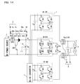
Embodiment 5 of the invention. - [FIG. 14] It is a schematic configuration view showing a power conditioner according to Embodiment 7 of the invention.
- [FIG. 15] It is a configuration view showing a bypass circuit according to Embodiment 7 of the invention.
- [FIG. 16] It is a configuration view showing another example of a bypass circuit according to Embodiment 7 of the invention.
- [FIG. 17] It is a configuration view showing second another example of a bypass circuit according to Embodiment 7 of the invention.
-
- 2
- third DC power source (solar light)
- 3
- boosting chopper circuit as booster circuit
- 4
- DC/DC converter
- 5
- system
- 7a, 7b
- chopper circuit
- 15, 15a to 15d
- output pulse
- 17
- output voltage
- 20
- bypass circuit
- 20a
- relay
- 100
- magnetic coupling core
- 3B-INV
- maximum single-phase inverter
- 1B-INV, 2B-INV
- single-phase inverter
- V3B
- maximum DC power source (voltage)
- V1B, V2B
- DC power source (voltage)
- L1, L2
- reactor
- Dz1A, Dz2A
- diode
- Qs, Qr
- switch
- Q11 to Q14, Q21 to Q24, Q31 to Q34
- switching device
- Q1B+Q2B
- quantity of charges as total quantity of power fluctuation
- Hereinafter, a power conversion apparatus (hereinafter referred to as power conditioner) according to
Embodiment 1 of the invention will be described with reference to the drawings.
FIG. 1 is a schematic configuration view showing a power conditioner according toEmbodiment 1 of the invention. As shown in FIG. 1, AC sides of plural (in this case, three) single-phase inverters 2B-INV, 3B-INV and 1B-INV are connected in series to form aninverter unit 1, which is a single-phase multiple converter. Each of the single-phase inverters 2B-INV, 3B-INV and 1B-INV includes plural self-turn-off semiconductor switching devices such as IGBTs with diodes connected in inverse-parallel. The single-phase inverter 1B-INV is connected to one of two terminals on the AC side of the single-phase inverter 3B-INV, which uses a DC power source V3B as its input, and the single-phase inverter 2B-INV is connected to the other terminal. Also, as short-circuit switches that form a short circuit between the two terminals on the AC sides of the single-phase inverter 3B-INV, two self-turn-off semiconductor switching devices Qx and Qy such as IGBTs, each of which having diodes connected in inverse-parallel, are connected parallel to the single-phase inverter 3B-INV. - Also, a boosting
chopper circuit 3 including a switching device (hereinafter referred to as switch) 3a such as IGBT, areactor 3b and adiode 3c is installed on a stage subsequent to aDC power source 2 based on solar light as a third DC power source. The boostingchopper circuit 3 boosts a DC voltage Vo acquired at theDC power source 2 and thus provides a voltage (potential Vc) charging a smoothing capacitor, which serves as the DC power source V3B.
The single-phase inverters 2B-INV, 3B-INV and 1B-INV convert DC power of the DC power sources V2B, V3B and V1B to AC power and output it. The DC power source of their inputs are connected by a DC-DC converter 4. The DC-DC converter 4 will be described later in detail. The voltages of the DC power sources V2B, V3B and V1B are described as V2B, V3B and V1B for convenience. - The voltage of the DC power source V3B, which serves as the input of the single-
phase inverter 3B-INV, is higher than the voltages of the DC power sources V2B and V1B, which serve as the inputs of the other single-phase inverters 2B-INV and 1B-INV. V2B, V3B and V1B are controlled to hold a predetermined voltage ratio by the DC-DC converter 4. Hereinafter, the DC power source V3B is referred to as maximum DC power source V3B, and the single-phase inverter 3B-INV is referred to as maximum single-phase inverter 3B-INV. Here, V1B = V2B ≥(2/9)×V3B holds. That is, the voltages of the DC power sources V1B and V2B of theinverters 1B-INV and 2B-INV are equal and the total of these two is equal to or larger than (4/9)×V3B.
These single-phase inverters 2B-INV, 3B-INV and 1B-INV can generate positive, negative and zero voltages as their outputs. Theinverter unit 1 outputs a voltage VA as the sum of these generated voltages combined, by gradational output voltage control operation. This output voltage VA is smoothed by a smoothingfilter 6 including areactor 6a and acapacitor 6b and an AC voltage Vout is supplied to asystem 5. It is assumed that thesystem 5 has its mid-point R grounded by a pole mounted transformer. - Next, the DC-
DC converter 4 connecting the DC power sources V2B, V3B and V1B will be described with reference to FIG. 2. FIG. 2 shows a circuit configuration including the DC-DC converter 4 of the power conditioner, but theDC power source 2 and the boostingchopper circuit 3 are not shown, for convenience. Here, the DC-DC converter 4 includeschopper circuits chopper circuit 7a is connected between the maximum DC power source V3B and the DC power source V1B, and thechopper circuit 7b is connected between the maximum DC power source V3B and the DC power source V2B. Thechopper circuits chopper circuit 7a operates, power is supplied from the maximum DC power source V3B to the DC power source V1B via the maximum single-phase inverter 3B-INV and the single-phase inverter 1B-INV. As thechopper circuit 7b operates, power is supplied from the maximum DC power source V3B to the DC power source V2B via the maximum single-phase inverter 3B-INV and the single-phase inverter 2B-INV. Also, diodes Dz1B, Dz2B are arranged to prevent a current from flowing backward directly to each potential of the DC power source V1B and DC power source V2B from the potential of the maximum DC power source V3B. - The operations of the single-
phase inverters 2B-INV, 3B-INV and 1B-INV, and thechopper circuits phase inverter 1B-INV is equal to the output of the single-phase inverter 2B-INV, and the single-phase inverters 1B-INV and 2B-INV are PWM-controlled to produce outputs in order to compensate for the difference between the target output voltage and the output voltage of the maximum single-phase inverter 3B-INV. Practically, they are controlled to flow a current into thesystem 5. However, in the case where theoutput reactor 6a is small, the difference between the voltage acquired by averaging the output voltage VA of theinverter unit 1 and the system voltage is small, and these can be considered almost the same. - During the period when switching devices Q31 and Q32 of the maximum single-
phase inverter 3B-INV are turned on and the maximum single-phase inverter 3B-INV is outputting a negative voltage, the switch Qs of thechopper circuit 7a is turned on and off. During a period TS1 in this period, the single-phase inverter 1B-INV outputs a negative voltage under PWM control, and a switching device Q12 is turned on and switching devices Q11 and Q14 are alternately turned on. During this period TS1, since the switching devices Q31 and Q12 are on, as the switch Qs is turned on and off, the reactor L1 is charged with a current iL1 flowing from the maximum DC power source V3B through the switching devices Q31 and Q12. Power is supplied to the DC power source V1B by a current iL1x flowing from the reactor L1 through the diode Dz1A. - During a period TS2 in the period when the switching devices Q31 and Q32 are on, the single-
phase inverter 1B-INV outputs a positive voltage under PWM control, and a switching device Q13 is turned on and the switching devices Q11 and Q14 are alternately turned on. During this period TS2, as the switch Qs is turned on and off, the reactor L1 is charged with a current iL1 flowing from the maximum DC power source V3B through the switching device Q31, the inverse-parallel diodes of the switching device Q13, and the DC power source V1B. Power is supplied to the DC power source V1B by a current iL1x flowing from the reactor L1 through the diode Dz1A.
In this manner, when the switching device Q31 of the maximum single-phase inverter 3B-INV is on and the positive electrode of the maximum DC power source V3B is connected to an AC output power line, as the switch Qs of thechopper circuit 7a is turned on and off, power can be supplied to the DC power source V1B from the maximum DC power source V3B via the maximum single-phase inverter 3B-INV and the single-phase inverter 1B-INV. - Meanwhile, during the period when switching devices Q33 and Q34 of the maximum single-
phase inverter 3B-INV are turned on and the maximum single-phase inverter 3B-INV is outputting a positive voltage, the switch Qr of thechopper circuit 7b is turned on and off. During a period Tr1 in this period, the single-phase inverter 2B-INV outputs a positive voltage under PWM control, and a switching device Q24 is turned on and switching devices Q22 and Q23 are alternately turned on. During this period Tr1, since the switching devices Q33 and Q24 are on, as the switch Qr is turned on and off, the reactor L2 is charged with a current iL2 flowing from the maximum DC power source V3B through the switching devices Q33 and Q24. Power is supplied to the DC power source V2B by a current iL2x flowing from the reactor L2 through the diode Dz2A. - During a period Tr2 in the period when the switching devices Q33 and Q34 are on, the single-
phase inverter 2B-INV outputs a negative voltage under PWM control, and a switching device Q21 is turned on and the switching devices Q22 and Q23 are alternately turned on. During this period Tr2, as the switch Qr is turned on and off, the reactor L2 is charged with a current iL2 flowing from the maximum DC power source V3B through the switching device Q33, the inverse-parallel diodes of the switching device Q21, and the DC power source V2B. Power is supplied to the DC power source V2B by a current iL2x flowing from the reactor L2 through the diode Dz2A.
In this manner, when the switching device Q33 of the maximum single-phase inverter 3B-INV is on and the positive electrode of the maximum DC power source V3B is connected to an AC output power line, as the switch Qr of thechopper circuit 7b is turned on and off, power can be supplied to the DC power source V2B from the maximum DC power source V3B via the maximum single-phase inverter 3B-INV and the single-phase inverter 2B-INV. - During the period when the output voltage of the maximum single-
phase inverter 3B-INV is zero, the semiconductor switches Qx and Qy that form a short circuit between the two terminals on the AC side of the maximum single-phase inverter 3B-INV are turned on into continuity and all the semiconductor switches Q31 to Q34 of the maximum single-phase inverter 3B-INV are turned off. In this case, since the single-phase inverter 1B-INV and the single-phase inverter 2B-INV are caused to operate to have the same output, the potential at the mid-point X of the maximum DC power source V3B is substantially equal to the ground potential, which is the intermediate potential of the output voltage Vout of the power conditioner. - As described above, in this embodiment, an output voltage waveform that is accurately close to a sine wave can be provided by the combination of the generated voltages of the single-
phase inverters 2B-INV, 3B-INV and 1B-INV. The smoothingfilter 6 on the output side can be configured with a small capacity or it can be omitted, and the configuration of the apparatus can be miniaturized. Also, the maximum single-phase inverter 3B-INV, which uses as its DC power source the DC voltage V3B boosted from the solar light voltage Vo by the boostingchopper circuit 3, and the single-phase inverters 2B-INV and 1B-INV, which use the DC power sources V1B and V2B supplied from this maximum DC power source V3B as their inputs, are connected to configure the power conditioner so that an output voltage is provided by using the sum of the generated voltages of the single-phase inverters. Therefore, a higher voltage than the DC voltage V3B boosted by the boostingchopper circuit 3 can be outputted efficiently. - Moreover, the DC-
DC converter 4 is formed by thechopper circuits chopper circuits - Also, during the period when the switching devices Q31 and Q33 are on so that the maximum single-
phase inverter 3B-INV connects the positive electrode of the maximum DC power source V3B to the AC output power line, thechopper circuits - Moreover, since the single-
phase inverters 2B-INV and 1B-INV are arranged and connected to both sides of the maximum single-phase inverter 3B-INV, which is at the center between them, power can be supplied easily and effectively from the maximum DC power source V3B of the maximum single-phase inverter 3B-INV to the DC power sources V1B and V2B of the single-phase inverters 2B-INV and 1B-INV on the both sides of theinverter 3B-INV. - Next, a power conditioner according to
Embodiment 2 of the invention will be described hereinafter with reference to FIG. 4. As shown in FIG. 4, as in theabove Embodiment 1, the DC-DC converter 4 is formed by thechopper circuits chopper circuits magnetic coupling core 100 made of a magnetic material.
The configuration except for the magnetic coupling of the reactors L1 and L2 is similar to theabove Embodiment 1. Also, FIG. 4 does not show theDC power source 2 and the boostingchopper circuit 3, for convenience. - Next, the operation will be described.
As described in theabove Embodiment 1, when the maximum single-phase inverter 3B-INV outputs a negative voltage, the switch Qs of thechopper circuit 7a is turned on and off to supply power to the DC power source V1B. However, the energy accumulated in the reactor L1 by the operation of thechopper circuit 7a can be shifted to the reactor L2 of thechopper circuit 7b at the rate of the magnetic coupling. Therefore, the energy can be used both by thechopper circuits phase inverter 3B-INV outputs a positive voltage, the switch Qr of thechopper circuit 7b is turned on and off and the energy accumulated in the reactor L2 is shifted to the reactor L1 at the rate of the magnetic coupling. Thus, power can be supplied not only to the DC power source V2B but also to the DC power source V1B . - In the power conditioner described in the
above Embodiment 1, the DC power sources V1B and V2B are supplied with power only during a half-period of one basic AC wave cycle. However, in this embodiment, the DC power sources V1B and V2B can be charged during the period when the maximum single-phase inverter 3B-INV is outputting, all the time during one basic AC wave cycle. Therefore, the rate of use of the DC-DC converter 4 (chopper circuits
Also, in theabove Embodiment 1, thechopper circuits magnetic coupling core 100 may be small. Moreover, compared with theabove Embodiment 1, where the DC power sources V1B and V2B are alternately supplied with power every half-period, imbalance between the voltages of the DC power source V1B and the DC power source V2B can be restrained and fluctuation of the mid-point potential of the maximum single-phase inverter 3B-INV can be restrained. Thus, in the case where the maximum DC power source V3B is connected to the solar battery (DC power source 2), occurrence of a leakage current can be restrained. - A case where the polarities of electromotive forces inducted by the reactors L1 and L2 are in the same direction in the power conditioner according the
above Embodiment 2 will be described hereinafter with reference to FIG. 5.
As shown in FIG. 5, the reactors L1 and L2 of thechopper circuits magnetic coupling core 100 made of a magnetic material. In this case, the reactors L1 and L2 have their windings formed in such a manner that the polarities of electromotive forces induced by the two reactors L1 and L2 are in the same direction. - The operations of the single-
phase inverters 2B-INV, 3B-INV and 1B-INV, and thechopper circuits above Embodiment 1, the output of the single-phase inverter 1B-INV and the output of the single-phase inverter 2B-INV are equal, and the single-phase inverters 1B-INV and 2B-INV are caused to produce outputs under PWM control in order to compensate for the difference between the target output voltage and the output voltage of the maximum single-phase inverter 3B-INV.
When the switching devices Q31 and Q32 of the maximum single-phase inverter 3B-INV are turned on and the maximum single-phase inverter 3B-INV is outputting a negative voltage, the switch Qs of thechopper circuit 7a is turned on and off. During a period TS1 in this period, the single-phase inverter 1B-INV outputs a negative voltage under PWM control, and during a period TS2, the single-phase inverter 1B-INV outputs a positive voltage under PWM control. In both periods, as the switch Qs is turned on and off, the DC power sources V1B and V2B are supplied with power from the maximum DC power source V3B in the following manner. - When the switch Qs is on, during the period TS1, a current iL1 flows from the maximum DC power source V3B through the switching devices Q31 and Q12, and during the period TS2, a current iL1 flows from the maximum DC power source V3B through the switching device Q31, the inverse-parallel diodes of the switching device Q13 , and the DC power source V1B . This current iL1 charges the reactor L1 of the
chopper circuit 7a and accumulates energy there, and the energy is shifted also to the reactor L2 of thechopper circuit 7b, which is magnetically connected with the reactor L1. At this time, a voltage of the same polarity is generated in the reactor L2 as in the reactor L1. However, since the diode Dz2A interrupts the current, a current iL2 will not be generated.
When the switch Qs is turned off, the reactors L1 and L2 cause currents iL1x and iL2x based on the accumulated energy, respectively, and supply power to the DC power sources V1B and V2B. In this manner, as the switch Qs of thechopper circuit 7a is switched, power can be supplied to the DC power sources V1B and V2B of the two single-phase inverters 1B-INV and 2B-INV. - When the switching devices Q33 and Q34 of the maximum single-
phase inverter 3B-INV are turned on and the maximum single-phase inverter 3B-INV is outputting a positive voltage, the switch Qr of thechopper circuit 7b is turned on and off. During a period Tr1 in this period, the single-phase inverter 2B-INV outputs a positive voltage under PWM control, and during a period Tr2, the single-phase inverter 2B-INV outputs a negative voltage under PWM control. In both periods, as the switch Qr is turned on and off, the DC power sources V1B and V2B are supplied with power from the maximum DC power source V3B in the following manner. - When the switch Qr is on, during the period Tr1, a current iL2 flows from the maximum DC power source V3B through the switching devices Q33 and Q24, and during the period Tr2, a current iL2 flows from the maximum DC power source V3B through the switching device Q33, the inverse-parallel diodes of the switching device Q21, and the DC power source V2B. This current iL2 charges the reactor L2 of the
chopper circuit 7b and accumulates energy there, and the energy is shifted also to the reactor L1 of thechopper circuit 7a, which is magnetically connected with the reactor L2. At this time, a voltage of the same polarity is generated in the reactor L1 as in the reactor L2. However, since the diode Dz1B interrupts the current, a current iL1 will not be generated.
When the switch Qr is turned off, the reactors L1 and L2 cause currents iL1x and iL2x based on the accumulated energy, respectively, and supply power to the DC power sources V1B and V2B. In this manner, as the switch Qr of thechopper circuit 7b is switched, power can be supplied to the DC power sources V1B and V2B of the two single-phase inverters 1B-INV and 2B-INV. - Next, a case where the polarities of electromotive forces induced by the reactors L1 and L2 are in the opposite directions in the power conditioner according to the
above Embodiment 2 will be described hereinafter with reference to FIG. 7.
As shown in FIG. 7, the reactors L1 and L2 of thechopper circuits magnetic coupling core 100 made of a magnetic material. In this case, the windings of the reactors L1 and L2 are formed in such a manner that the polarities of electromotive forces induced by the two reactors L1 and L2 are in the opposite directions, and a gap is provided in themagnetic coupling core 100 to adjust the strength of the magnetic coupling. - The operation of supplying power to the DC power sources V1B and V2B from the maximum DC power source V3B in the power conditioner shown in FIG. 7 will be described hereinafter.
When the switching devices Q31 and Q32 of the maximum single-phase inverter 3B-INV are on and the maximum single-phase inverter 3B-INV is outputting a negative output, if the switch Qs of thechopper circuit 7a is turned on and off, the reactor L1 is charged, but a voltage of the opposite polarity to the reactor L1 is generated in the reactor L2. By this voltage generated in the reactor L2, a current iL2x is caused to flow via the diode Dz2A to supply power to the DC power source V2B. The operation of supplying power to the DC power source V1B in this case is similar to the case shown in FIG. 5.
Although the DC power source V2B can be charged by the voltage generated in the reactor L2, if the voltage difference between the DC power source V3B and the DC power source V2B is large, a rush current flows into the DC power source V2B. Thus, to prevent this, the gap provided in themagnetic coupling core 100 adjusts the strength of the magnetic coupling between the reactor L1 and the reactor L2. - Similarly, when the maximum single-
phase inverter 3B-INV is outputting a positive voltage, if the switch Qr of thechopper circuit 7b is turned on and off, the reactor L2 is charged, and a voltage of the opposite polarity to the reactor L1 is generated in the reactor L1. By this voltage generated in the reactor L1, power is supplied to the DC power source V1B and both the DC power sources V1B and V2B can thus be supplied with power. Also in this case, the gap provided in themagnetic coupling core 100 prevents a rush current from flowing into the DC power source V1B. - In the above Embodiments 1 and 2, the maximum single-
phase inverter 3B-INV is arranged at the center. A case where the inverters are arranged in ascending order of the voltages of DC power sources V1B, V2B and V3B that serve as their inputs, will be described hereinafter with reference to FIG. 8.
Also in this case, the maximum DC power source V3B of the maximum single-phase inverter 3B-INV is generated as the DC voltage Vo acquired at theDC power source 2 based on solar light as the third DC power source is boosted by the boostingchopper circuit 3. In FIG. 8, theDC power source 2 and the boostingchopper circuit 3 are not shown, for convenience. The voltages V1B, V2B and V3B of the DC power sources are controlled to hold a predetermined voltage ratio by the DC-DC converter 4 (see FIG. 1). Here, V1B:V2B:V3B = 1:3:9 holds. - The DC-
DC converter 4 includeschopper circuits chopper circuit 7a is connected between the DC power source V2B and the DC power source V1B, and thechopper circuit 7b is connected between the maximum DC power source V3B and the DC power source V2B. Thechopper circuits chopper circuit 7b operates, power is supplied from the maximum DC power source V3B to the DC power source V2B via the maximum single-phase inverter 3B-INV and the single-phase inverter 2B-INV. As thechopper circuit 7a operates, power is supplied from the DC power source V2B to the DC power source V1B via the single-phase inverter 2B-INV and the single-phase inverter 1B-INV. Also, diodes Dz1B, Dz2B are arranged to prevent a current from flowing backward directly from the potential of the DC power source V2B to the potential of the DC power source V1B and from the potential of the maximum DC power source V3B to the potential of the DC power source V2B. - The operations of the single-
phase inverters 1B-INV, 2B-INV and 3B-INV, and thechopper circuits phase inverters 1B-INV and 2B-INV are PWM-controlled to produce outputs in order to compensate for the difference between the target output voltage and the output voltage of the maximum single-phase inverter 3B-INV. Here, it is described that the output of the single-phase inverter 1B-INV and the output of the single-phase inverter 2B-INV are equal, but it is not limited to this.
When switching devices Q33 and Q34 of the maximum single-phase inverter 3B-INV are turned on and the maximum single-phase inverter 3B-INV is outputting a positive voltage, the switch Qr of thechopper circuit 7b is turned on and off. During a period Tr1 in this period, the single-phase inverter 2B-INV outputs a positive voltage under PWM control, and a switching device Q24 is turned on and switching devices Q22 and Q23 are alternately turned on. During this period Tr1, since the switching devices Q33 and Q24 are on, as the switch Qr is turned on and off, the reactor L2 is charged with a current iL2 flowing from the maximum DC power source V3B through the switching devices Q33 and Q24. Power is supplied to the DC power source V2B by a current iL2x flowing from the reactor L2 through the diode Dz2A. - During a period Tr2 in the period when the switching devices Q33 and Q34 are on, the single-
phase inverter 2B-INV outputs a negative voltage under PWM control, and a switching device Q21 is turned on and the switching devices Q22 and Q23 are alternately turned on. During this period Tr2, as the switch Qr is turned on and off, the reactor L2 is charged with a current iL2 flowing from the maximum DC power source V3B through the switching device Q33, the inverse-parallel diodes of the switching device Q21, and the DC power source V2B. Power is supplied to the DC power source V2B by a current iL2x flowing from the reactor L2 through the diode Dz2A.
In this manner, when the switching device Q33 of the maximum single-phase inverter 3B-INV is on and the positive electrode of the maximum DC power source V3B is connected to an AC output power line, as the switch Qr of thechopper circuit 7b is turned on and off, power can be supplied to the DC power source V2B from the maximum DC power source V3B via the maximum single-phase inverter 3B-INV and the single-phase inverter 2B-INV. - Meanwhile, when the single-
phase inverter 2B-INV is outputting a positive or negative voltage, the switch Qs of thechopper circuit 7a is turned on and off. During a period TS1 and a period TS3 in this period, each of the single-phase inverters 1B-INV and 2B-INV outputs a positive voltage under PWM control, and switching devices Q14 and Q24 are turned on and switching devices Q12 and Q13 and the switching devices Q22 and Q23 are alternately turned on. During these periods TS1 and TS3, when the switching devices Q23 and Q14 are on, as the switch Qs is turned on and off, the reactor L1 is charged with a current iL1 flowing from the DC power source V2B through the switching devices Q23 and Q14. Power is supplied to the DC power source V1B by a current flowing from the reactor L1 through the diode Dz1A. - Also, during the period TS2, each of the single-
phase inverters 1B-INV and 2B-INV outputs a negative voltage under PWM control, and switching devices Q11 and Q21 are turned on and the switching devices Q12 and Q13 and the switching devices Q22 and Q23 are alternately turned on. During this period TS2, when the switching device 23 is on, as the switch Qs is turned on and off, the reactor L1 is charged with a current iL1 flowing from the DC power source V2B through the switching device Q23, the inverse-parallel diodes of the switching device Q11, and the DC power source V1B. Power is supplied to the DC power source V1B by a current flowing from the reactor L1 through the diode Dz1A.
In this manner, when the switching device Q23 of the single-phase inverter 2B-INV is on and the positive electrode of the DC power source V2B is connected to an AC output power line, as the switch Qs of thechopper circuit 7a is turned on and off, power can be supplied to the DC power source V1B from the DC power source V2B via the single-phase inverter 2B-INV and the single-phase inverter 1B-INV. - In this embodiment, too, a power conditioner with improved conversion efficiency and with a small and inexpensive configuration can be provided.
Also, in this embodiment, the maximum single-phase inverter 3B-INV is arranged at an end, and power is supplied from the maximum DC power source V3B of the maximum single-phase inverter 3B-INV to the DC power source V2B of the single-phase inverter 2B-INV connected next to theinverter 3B-INV. Moreover, power is supplied from the DC power source V2B of the single-phase inverter 2B-INV to the DC power source V1B of the single-phase inverter 1B-INV connected next to theinverter 2B-INV. Since the DC power sources V2B and V1B other than the maximum DC power source V3B are supplied with power from the DC power sources V3B and V2B of the single-phase inverters 3B-INV and 2B-INV connected next to each other in the direction toward higher voltage of the DC power sources, the DC power sources V2B and V1B other than the maximum DC power source V3B can be supplied with power easily and securely, and the voltages of the DC power sources V1B and V2B can be set. - In the
above Embodiment 3, three single-phase inverters are used, but two, four or more may be used. If these inverters are arranged in ascending or descending order of voltages of the DC power sources that serve as their inputs and the maximum single-phase inverter is arranged at an end, the DC power sources other than the maximum DC power source can be supplied with power easily and securely, as in the above embodiment. - In the above embodiments, the DC-
DC converter 4 is formed by thechopper circuits
Three exemplary configurations of the bidirectional DC-DC converter that connects the DC power sources V1B, V2B and V3B are shown in FIG. 10 to FIG. 12.
A bidirectional DC-DC converter 11 shown in FIG. 10(a) includes transformers and switches Qd1, Qd2 and Qd3. Windings 11a, 11b and 11c of the transformers connected to the DC power sources V1B, V2B and V3B are connected in such a manner that a forward converter is formed between the maximum DC power source V3B and the DC power source V2B and a fly-back converter is formed between the maximum DC power source V3B and the DC power source V1B. Their DC voltage ratio is V1B:V2B:V3B = 1 : 3 : 9 . - FIG. 10(b) shows gate voltages that serve as driving signals of the switches Qd1, Qd2 and Qd3.
The gate voltage of the switch Qd3 and the gate voltage of the switch Qd1 are in the inverse relation, and the relation between the voltages V3B and V1B is defined as 9: 1 by the values of Td and the ratio of the number of turns of the transformers. In this case, if the relation between the voltages V3B and V1B is V3B>9V1B, power is transmitted from the maximum DC power source V3B to the DC power source V1B, and if it is V3B<9V1B, power is transmitted from the DC power source V1B to the maximum DC power source V3B.
Also, the gate voltage of the switch Qd3 and the gate voltage of the switch Qd2 are the same, and the relation between the voltages V3B and V2B is defined as 3:1 by the value of only the ratio of the number of turns of the transformers. In this case, if the relation between the voltages V3B and V2B is V3B>3V2B, power is transmitted from the maximum DC power source V3B to the DC power source V2B, and if it is V3B<3V2B, power is transmitted from the DC power source V2B to the maximum DC power source V3B.
Since V1B can be controlled by changing Td and V2B is decided by the ratio of the number of turns of the transformers, both of the voltages V1B and V2B can be set at predetermined values. In such a bidirectional DC-DC converter 11, since the fly-back converter is connected between the maximum DC power source V3B and the DC power source V1B, the voltages of the DC power source V1B and V2B can be set by using a small number of devices. - A bidirectional DC-
DC converter 12 shown in FIG. 11(a) includes transformers, switches Qd1, Qd2 and Qd3, and a reset winding 13. Windings 12a, 12b and 12c of the transformers connected to the DC power sources V1B, V2B and V3B are connected in such a manner that a forward converter is formed between the maximum DC power source V3B and the DC power source V2B and between the maximum DC power source V3B and the DC power source V1B.
FIG. 11(b) shows gate voltages that serve as driving signals of the switches Qd1, Qd2 and Qd3.
The gate voltages of the switches Qd1, Qd2 and Qd3 are the same and the relation between the voltages V1B, V2B and V3B is defined as 1:3:9 by the value of only the ratio of the number of turns of the transformers. In this case, if it is V3B>9V1B, power is transmitted from the maximum DC power source V3B to the DC power source V1B, and if it is V3B<9V1B, power is transmitted from the DC power source V1B to the maximum DC power source V3B. Also, if it is V3B>3V2B, power is transmitted from the maximum DC power source V3B to the DC power source V2B, and if it is V3B<3V2B, power is transmitted from the DC power source V2B to the maximum DC power source V3B. Thus, both of the voltages V1B and V2B can be set at predetermined values.
In such a bidirectional DC-DC converter 12, the forward converter is formed between the maximum DC power source V3B and the DC power source V1B, and between the maximum DC power source V3B and the DC power source V2B. Then the processing of excitation fluxes is carried out by the reset winding 13 near the maximum DC power source V3B. Therefore, an excitation current can be reduced and core loss can be reduced. - A bidirectional DC-
DC converter 14 shown in FIG. 12(a) includes transformers and switches Qd1, Qd2 and Qd3. Windings 14a, 14b and 14c of the transformers connected to the DC power sources V1B, V2B and V3B are connected in such a manner that a fly-back converter is formed between the maximum DC power source V3B and the DC power source V2B and between the maximum DC power source V3B and the DC power source V1B.
FIG. 12(b) shows gate voltages that serve as driving signals of the switches Qd1, Qd2 and Qd3.
The gate voltage of the switch Qd3 and the gate voltages of the switches Qd1 and Qd2 are in the inverse relation, and the relation between the voltages V1B, V2B and V3B is defined as 1:3:9 by the values of Td and the ratio of the number of turns of the transformers.
In this case, V1B and V2B can be securely controlled by changing Td. Thus, both of the voltages V1B and V2B can be stably controlled at predetermined values. - In the
above Embodiment 1, the DC-DC converter 4 formed by thechopper circuits
In such a unidirectional DC-DC converter 4, power cannot be transmitted from the DC power sources V2B and V1B even when the voltage ratio of V1B and V2B increases. However, in this embodiment, the output pulse width of the maximum single-phase inverter 3B-INV is adjusted and the quantities of power of the DC power sources V2B and V1B are thus adjusted, as shown in FIG. 13.
Here, it is assumed that the maximum value (peak value) of the AC voltage Vout outputted from the power conditioner is Vm, and that the rate of voltage use is equal to Vm/ (V1B+V2B+V3B) . The relation between this rate of voltage use and the quantity of power fluctuation in the DC power sources V1B and V2B calculated by subtracting the quantity of charging from the quantity of discharging via the respective inverters will be described hereinafter. Q1B and Q2B are the quantities of charges that have flowed out of the DC power sources V1B and V2B due to discharging and charging via the single-phase inverters 1B-INV, 2B-INV and 3B-INV. It is known that when the voltage ratio of the DC power sources V1B, V2B and V3B of the respective inverters is 1:3:9, if a current of sine wave with a power factor of 1 is caused to flow to a load connected to the power conditioner, the quantity of outflow charges (Q1B+Q2B), which is the total quantity of power fluctuation of the DC power sources V1B and V2B becomes zero at a rate of voltage use P (= about 0.83). - As shown in FIG. 13(a), when the output voltage Vc (V3B) of the boosting
chopper circuit 3 of the power conditioner is about 235 V, the rate of voltage use is about 0.83 and the quantity of outflow charges (Q1B+Q2B) from the DC power sources V1B and V2B is close to zero. A numeral 15 represents the output pulse of the maximum single-phase inverter 3B-INV, a numeral 16 represents the total output from the single-phase inverters 1B-INV and 2B-INV, and a numeral 17 represents the AC output voltage Vout from the power conditioner.
Next, as shown in FIG. 13(b), when the voltage of solar light is lowered by a rise in the ambient temperature or the like and the output voltage Vc (V3B) of the boostingchopper circuit 3 of the power conditioner is, for example, about 204 V, the rate of voltage use is about 0.95 and the quantity of outflow charges (Q1B+Q2B) from the DC power sources V1B and V2B increases. In such a case, if the output pulse width of the maximum single-phase inverter 3B-INV is increased, the power load of the single-phase inverters 1B-INV and 2B-INV is reduced and (Q1B+Q2B) becomes closer to zero. Numerals 15a and 15b represent the output pulse of the maximum single-phase inverter 3B-INV before and after the adjustment of the pulse width, andnumerals phase inverters 1B-INV and 2B-INV before and after the adjustment of the pulse width. - Next, as shown in FIG. 13(c), when the voltage of solar light rises because of a drop in the ambient temperature or the like and the output voltage Vc (V3B) of the boosting
chopper circuit 3 of the power conditioner is, for example, about 260 V, the rate of voltage use is about 0.75 and the quantity of outflow charges (Q1B+Q2B) from the DC power sources V1B and V2B becomes negative. In such a case, if the output pulse width of the maximum single-phase inverter 3B-INV is narrowed, the power load of the single-phase inverters 1B-INV and 2B-INV increases and (Q1B+Q2B) becomes positive. Numerals 15c and 15d represent the output pulse of the maximum single-phase inverter 3B-INV before and after the adjustment of the pulse width, andnumerals phase inverters 1B-INV and 2B-INV before and after the adjustment of the pulse width. - In this manner, the power load of the single-
phase inverters 1B-INV and 2B-INV can be easily adjusted by the increase or decrease of the output pulse width of the maximum single-phase inverter 3B-INV. Therefore, the quantity of outflow charges (Q1B+Q2B) from the DC power sources V1B and V2B can be easily adjusted. In this case, if the single-phase inverters 1B-INV and 2B-INV are set to have DC voltages that are necessary for acquiring the total output of the single-phase inverters 1B-INV and 2B-INV, a predetermined output can be provided.
Thus, as shown in FIG. 13(c), even when Vc(V3B) rises and (Q1B+Q2B) becomes negative, the output pulse width of the maximum single-phase inverter 3B-INV can be narrowed to make (Q1B+Q2B) positive or zero. Thus, power need not be supplied from the DC power sources V1B and V2B to the maximum DC power source V3B, and the voltages of the DC power sources V1B and V2B can be stably controlled by using the unidirectional DC-DC converter 4 that only supplies power from the maximum DC power source V3B. - Moreover, as described above, since (Q1B+Q2B) can be easily adjusted by the increase or decrease of the output pulse width of the maximum single-
phase inverter 3B-INV, (Q1B+Q2B) can be easily made closer to zero. Therefore, the power handled by the DC-DC converter 4 can easily be made closer to zero and efficiency improves. Such control can also be applied to theabove Embodiment 4. The power handled by the bidirectional DC-DC converters - Next, the power conditioner having the similar circuit configuration shown in FIG. 1 in the
above Embodiment 1, with improved efficiency of the boostingchopper circuit 3, will be described hereinafter.
Meanwhile, the maximum output voltage necessary for an AC output of 200 V is approximately 282 V. The output voltage VA of theinverter unit 1 can be V1B+V2B+V3B at the maximum. Therefore, if V1B+V2B+V3B is approximately 282 V or higher, the power conditioner can provide an AC output of 200 V. V1B+V2B+V3B is larger than V3B, which is the voltage boosted by the boostingchopper circuit 3. For example, if the relation between V1B, V2B and V3B is 2:2:9, V1B+V2B+V3B is 13/9 times V3B. That is, when V3B is about 195 V or higher, V1B+V2B+V3B is 282 V or higher and this is the condition for an AC output. - If the solar light voltage Vo is 195 V or higher, V3B is about 195 V or higher and a predetermined AC output can be provided without the boosting operation by the boosting
chopper circuit 3. Therefore, in this embodiment, theIGBT switch 3a is turned on and off until the DC voltage (solar light voltage) Vo acquired at theDC power source 2 reaches a predetermined voltage Vm1 (195 V), and the voltage is thus boosted to the voltage Vm1. When the predetermined voltage Vm1 is exceeded, theIGBT switch 3a is stopped to stop the boosting operation of the boostingchopper circuit 3.
As the solar light voltage Vo increases, the boosting rate is lowered and the efficiency of the boostingchopper circuit 3 improves. However, when theIGBT switch 3a is stopped, the loss is significantly reduced and there is only a continuity loss of thediode 3c. Moreover, as the solar light voltage Vo increases, the current is lowered and the continuity loss in thediode 3c is reduced. - In this embodiment, when the solar light voltage Vo exceeds a predetermined voltage Vm1 (195 V), the
IGBT switch 3a is stopped to stop the boosting operation. Therefore, the loss due to boosting can be significantly reduced as described above, and a power conditioner with high conversion efficiency can be provided. The predetermined voltage Vm1 at which the boosting operation is to stop may be about 195 V or higher, but the loss of the boostingchopper circuit 3 can be reduced further at a lower voltage. - FIG. 14 is a schematic configuration view showing a power conditioner according to Embodiment 7 of the invention. The power conditioner according to this embodiment is configured by providing a
bypass circuit 20 that bypasses the boostingchopper circuit 3 in the power conditioner shown in FIG. 1 of theabove Embodiment 1.
As shown in FIG. 14, the boostingchopper circuit 3 boosts a DC voltage Vo acquired at theDC power source 2, and V3B, which is the voltage of the maximum DC power source V3B, is provided. Also, to bypass the boostingchopper circuit 3 when stopping the boosting, thebypass circuit 20 including, for example, arelay 20a, is connected parallel to the boostingchopper circuit 3. - In the boosting
chopper circuit 3, as in theabove Embodiment 6, theIGBT switch 3a is turned on and off until the DC voltage (solar light voltage) Vo acquired at theDC power source 2, which serves as its input, reaches a predetermined voltage Vm1 (195 V), and it is thus boosted to the voltage Vm1. During this time, therelay 20a of thebypass circuit 20 is left open. Then, theIGBT switch 3a is stopped when the predetermined voltage Vm1 is exceeded. At this point, therelay 20a of thebypass circuit 20 is closed and a current is caused to flow to the side of thebypass circuit 20, thus bypassing thereactor 3b and thediode 3c of the boostingchopper circuit 3. - In the range where the solar light voltage Vo is equal to or less than the predetermined voltage Vm1, the boosting
chopper circuit 3 carries out boosting so that the output voltage V3B becomes the predetermined voltage Vm1. Therefore, as the solar light voltage Vo increases, the boosting rate is lowered and the efficiency of the boostingchopper circuit 3 improves. When the solar light voltage Vo exceeds the predetermined voltage Vm1, the boosting operation stops and therelay 20a of thebypass circuit 20 is closed to cause a current to flow to the side of thebypass circuit 20. Therefore, there is little loss. Thus, the efficiency of the boostingchopper circuit 3 suddenly increases from the point where the solar light voltage Vo reaches the voltage Vm1. - The predetermined voltage Vm1 at which the boosting operation should be stopped may be approximately 195 V or higher. However, a lower voltage enables further reduction in the power loss in the
chopper circuit 3. After the boosting operation is stopped, not only the loss can be significantly reduced by the stop of theIGBT switch 3a, but also the continuity loss of thereactor 3b and thediode 3c can be eliminated by bypassing thereactor 3b and thediode 3c in the boostingchopper circuit 3. There is almost no loss in the boostingchopper circuit 3. Therefore, a power conditioner with high conversion efficiency can be provided. - The
bypass circuit 20 in the above Embodiment 7 will be described in detail hereinafter with reference to FIG. 15 to FIG 17.
Thebypass circuit 20 includes therelay 20a and bypasses one or both of thereactor 3b and thediode 3c connected in series in the boostingchopper circuit 3.
FIG. 15 shows abypass circuit 20 in which therelay 20a bypasses thereactor 3b and thediode 3c, as shown in FIG. 14 in the above Embodiment 7. FIG. 16 shows abypass circuit 20 according to another example, in which therelay 20a bypasses only thediode 3c. FIG. 17 shows abypass circuit 20 according to another example, in which therelay 20a bypasses only thereactor 3b. - Also, a self-turn-off
semiconductor switch 20b is connected parallel to therelay 20a. Since therelay 20a usually opens with zero current or a low voltage, a DC current is difficult to interrupt. However, it can be easily interrupted when thesemiconductor switch 20b is thus provided in parallel. In this case, thesemiconductor 20b is turned on at the same time as therelay 20a is opened, and the current is temporarily shifted to thesemiconductor switch 20b. Thus, the current flowing through therelay 20a is interrupted, and thesemiconductor switch 20b is turned off after that. - In any case, when the solar light voltage Vo exceeds the predetermined voltage Vm1, the
IGBT switch 3a is stopped to stop the boosting operation, and therelay 20a of thebypass circuit 20 is closed to cause the current to flow to the side of thebypass circuit 20.
In the case of FIG. 15, since thereactor 3b and thediode 3c in the boostingchopper circuit 3 are bypassed, the continuity loss of thereactor 3b and thediode 3c can be eliminated and the overall efficiency of the power conditioner increases.
In the case of FIG. 16, since only thediode 3c in the boostingchopper circuit 3 is bypassed, the continuity loss of thediode 3c can be eliminated and the overall efficiency of the power conditioner increases. In this case, since thereactor 3b is not bypassed, thereactor 3b can be used as a filter. - In FIG. 15 and FIG. 16, since the
diode 3c is bypassed, when the DC power source V3B gets higher than the solar light voltage Vo, reversal of the current occurs, and additionally, a reverse voltage is applied to the solar panel, which is theDC power source 2. There is a risk of damage to the panel. Therefore, a configuration is made that detects the current flowing through therelay 20a, and that opens therelay 20a when the current becomes a predetermined value or less, in order to switch to the current path via thereactor 3b and thediode 3c. As therelay 20a is thus opened to make the function of thediode 3c effective, the functions of preventing reversal of the current and of protecting the solar panel from the reverse voltage are provided.
When therelay 20a is opened, even if a reverse current has already been generated because of delay in detection, the current can be temporarily shifted to thesemiconductor switch 20b and thus can be securely interrupted. - In the case of FIG. 17, since only the
reactor 3b in the boostingchopper circuit 3 is bypassed, the continuity loss of thereactor 3b can be eliminated and the overall efficiency of the power conditioner increases. Also, since thediode 3c is not bypassed, reversal of the current can be prevented and the solar panel can be protected from the reverse voltage by thediode 3c, and reliability can be easily improved. In this case, therelay 20a can be shut off without having thesemiconductor switch 20b provided. However, as thesemiconductor switch 20b is provided, therelay 20a can also be shut off when anomaly occurs in thediode 3c. - The invention can be broadly applied to an uninterruptible power supply apparatus that boosts a DC voltage of a decentralized power source such as solar light to a required voltage and then converts it to AC and links it to a system, or an inverter apparatus that supplies AC power after conversion to a load.
Claims (16)
- A power conversion apparatus in which AC sides of plural single-phase inverters that convert DC power of DC power sources to AC power are connected in series, and in which an output voltage is controlled by using the sum of generated voltages from a predetermined combination selected from the plural single-phase inverters, the apparatus being characterized in that
first and second DC power sources that serve as inputs of first and second single-phase inverters having their AC sides connected next to each other, of the plural single-phase inverters, are connected to each other via a DC-DC converter, and
the DC-DC converter supplies power from the first DC power source having a higher voltage to the second DC power source having a lower voltage, via switching devices in the first and second single-phase inverters. - The power conversion apparatus according to claim 1, characterized in that the DC-DC converter is formed by a chopper circuit including a reactor, a rectifying device and a switch.
- The power conversion apparatus according to claim 2, characterized in that, during an operation period when the first single-phase inverter that uses the first DC power source as its input turns on switching devices that connect a positive electrode of the first DC power source to an AC output power line, the switch in the chopper circuit is turned on and off.
- The power conversion apparatus according to claim 2, characterized in that a maximum DC power source having the highest voltage of the DC power sources that serve as inputs of the plural single-phase inverters is generated from a third DC power source, and the maximum DC power source is assumed to be the first DC power source, and
both AC terminals of the first single-phase inverter using the first DC power source as its input are respectively connected to the second single-phase invertors, and the two second DC power sources have the chopper circuits, respectively, and are supplied with power from the first DC power source via the switching devices in the first and second single-phase inverters. - The power conversion apparatus according to claim 4, characterized in that an output pulse width of the single-phase inverter that uses the maximum DC power source as its input is adjusted, and a total quantity of power fluctuation calculated by subtracting a quantity of charging from a quantity of discharging via the single-phase inverters of the other DC power sources is caused to be positive or zero.
- The power conversion apparatus according to claim 5, characterized in that the output pulse width of the single-phase inverter is adjusted so that the total quantity of power fluctuation is reduced.
- The power conversion apparatus according to claim 4, characterized in that the two reactors in the two chopper circuits are magnetically coupled by a magnetic coupling core made of a magnetic material.
- The power conversion apparatus according to claim 7, characterized in that the two reactors are configured with windings so that the polarities of electromotive forces induced by the reactors are in the same direction.
- The power conversion apparatus according to claim 7, characterized in that the two reactors are configured with windings so that the polarities of electromotive forces induced by the reactors are in the opposite directions, and a gap to adjust the rate of magnetic coupling is provided in the magnetic coupling core.
- The power conversion apparatus according to claim 2, characterized in that the plural single-phase inverters are connected in ascending or descending order of voltages of DC power sources that serve as their inputs, and a maximum DC power source having the highest voltage of the plural DC power sources is generated from a third power source, and
first and second DC power sources that serve as inputs of each pair of the first and second single-phase inverters having their AC sides connected next to each other, of the plural single-phase inverters, are connected via the chopper circuits, respectively, and each of the chopper circuits supplies power from the first DC power source having the higher voltage to the second DC power source having the lower voltage of each pair via the switching devices in the first and second single-phase inverters, thereby allowing each of the DC power sources other than the maximum DC power source to be supplied with power. - The power conversion apparatus according to claim 10, characterized in that an output pulse width of the single-phase inverter that uses the maximum DC power source as its input is adjusted, and a total quantity of power fluctuation calculated by subtracting a quantity of charging from a quantity of discharging via the respective single-phase inverters of the other DC power sources is caused to be positive or zero.
- The power conversion apparatus according to claim 11, characterized in that the output pulse width of the single-phase inverter is adjusted so that the total quantity of power fluctuation is reduced.
- The power conversion apparatus according to claim 1, characterized in that a maximum DC power source having the highest voltage of the DC power sources that serve as inputs of the plural single-phase inverters is generated from a third DC power source via a boosting circuit, and when the voltage of the third DC power source exceeds a predetermined voltage, on-off operation of a switch in the boosting circuit is stopped to stop boosting operation.
- The power conversion apparatus according to claim 13, characterized in that a bypass circuit that bypasses the boosting circuit is provided, and
when the voltage of the third DC power source exceeds a predetermined voltage, on-off operation of the switch in the boosting circuit is stopped to stop boosting operation and the boosting circuit is bypassed by the bypass circuit. - The power conversion apparatus according to claim 14, characterized in that the bypass circuit includes a relay.
- The power conversion apparatus according to claim 1, characterized in that a predetermined AC voltage and AC current are outputted and supplied to a load, or the predetermined AC output is connected parallel to a system and linked to the system.
Applications Claiming Priority (2)
| Application Number | Priority Date | Filing Date | Title |
|---|---|---|---|
| JP2005050700 | 2005-02-25 | ||
| PCT/JP2006/303001 WO2006090675A1 (en) | 2005-02-25 | 2006-02-21 | Power converter |
Publications (3)
| Publication Number | Publication Date |
|---|---|
| EP1852964A1 true EP1852964A1 (en) | 2007-11-07 |
| EP1852964A4 EP1852964A4 (en) | 2011-03-09 |
| EP1852964B1 EP1852964B1 (en) | 2012-01-18 |
Family
ID=36927315
Family Applications (1)
| Application Number | Title | Priority Date | Filing Date |
|---|---|---|---|
| EP20060714141 Expired - Fee Related EP1852964B1 (en) | 2005-02-25 | 2006-02-21 | Power conversion apparatus |
Country Status (5)
| Country | Link |
|---|---|
| US (1) | US7596008B2 (en) |
| EP (1) | EP1852964B1 (en) |
| JP (1) | JP4527768B2 (en) |
| CN (1) | CN101128973B (en) |
| WO (1) | WO2006090675A1 (en) |
Cited By (2)
| Publication number | Priority date | Publication date | Assignee | Title |
|---|---|---|---|---|
| EP2365626A3 (en) * | 2010-03-10 | 2014-05-28 | Omron Corporation | Power converter and power conditioner |
| EP3484040A1 (en) * | 2017-11-09 | 2019-05-15 | CE+T Power Luxembourg SA | Inverter with ac forward bridge and improved dc/dc topology |
Families Citing this family (88)
| Publication number | Priority date | Publication date | Assignee | Title |
|---|---|---|---|---|
| US7719865B2 (en) * | 2005-02-25 | 2010-05-18 | Mitsubishi Electric Corporation | Power conversion apparatus |
| US10693415B2 (en) | 2007-12-05 | 2020-06-23 | Solaredge Technologies Ltd. | Testing of a photovoltaic panel |
| US11881814B2 (en) | 2005-12-05 | 2024-01-23 | Solaredge Technologies Ltd. | Testing of a photovoltaic panel |
| US11296650B2 (en) | 2006-12-06 | 2022-04-05 | Solaredge Technologies Ltd. | System and method for protection during inverter shutdown in distributed power installations |
| US8384243B2 (en) | 2007-12-04 | 2013-02-26 | Solaredge Technologies Ltd. | Distributed power harvesting systems using DC power sources |
| US11309832B2 (en) | 2006-12-06 | 2022-04-19 | Solaredge Technologies Ltd. | Distributed power harvesting systems using DC power sources |
| US8319483B2 (en) | 2007-08-06 | 2012-11-27 | Solaredge Technologies Ltd. | Digital average input current control in power converter |
| US11735910B2 (en) | 2006-12-06 | 2023-08-22 | Solaredge Technologies Ltd. | Distributed power system using direct current power sources |
| US8013472B2 (en) | 2006-12-06 | 2011-09-06 | Solaredge, Ltd. | Method for distributed power harvesting using DC power sources |
| US8618692B2 (en) | 2007-12-04 | 2013-12-31 | Solaredge Technologies Ltd. | Distributed power system using direct current power sources |
| US11569659B2 (en) | 2006-12-06 | 2023-01-31 | Solaredge Technologies Ltd. | Distributed power harvesting systems using DC power sources |
| US11687112B2 (en) | 2006-12-06 | 2023-06-27 | Solaredge Technologies Ltd. | Distributed power harvesting systems using DC power sources |
| US11728768B2 (en) | 2006-12-06 | 2023-08-15 | Solaredge Technologies Ltd. | Pairing of components in a direct current distributed power generation system |
| US8947194B2 (en) | 2009-05-26 | 2015-02-03 | Solaredge Technologies Ltd. | Theft detection and prevention in a power generation system |
| US8319471B2 (en) | 2006-12-06 | 2012-11-27 | Solaredge, Ltd. | Battery power delivery module |
| US11888387B2 (en) | 2006-12-06 | 2024-01-30 | Solaredge Technologies Ltd. | Safety mechanisms, wake up and shutdown methods in distributed power installations |
| US8816535B2 (en) | 2007-10-10 | 2014-08-26 | Solaredge Technologies, Ltd. | System and method for protection during inverter shutdown in distributed power installations |
| US9112379B2 (en) | 2006-12-06 | 2015-08-18 | Solaredge Technologies Ltd. | Pairing of components in a direct current distributed power generation system |
| US9130401B2 (en) | 2006-12-06 | 2015-09-08 | Solaredge Technologies Ltd. | Distributed power harvesting systems using DC power sources |
| US8473250B2 (en) | 2006-12-06 | 2013-06-25 | Solaredge, Ltd. | Monitoring of distributed power harvesting systems using DC power sources |
| US11855231B2 (en) | 2006-12-06 | 2023-12-26 | Solaredge Technologies Ltd. | Distributed power harvesting systems using DC power sources |
| US8963369B2 (en) | 2007-12-04 | 2015-02-24 | Solaredge Technologies Ltd. | Distributed power harvesting systems using DC power sources |
| US9088178B2 (en) | 2006-12-06 | 2015-07-21 | Solaredge Technologies Ltd | Distributed power harvesting systems using DC power sources |
| JP5049637B2 (en) * | 2007-04-12 | 2012-10-17 | 三菱電機株式会社 | DC / DC power converter |
| EP3324505B1 (en) | 2007-10-15 | 2023-06-07 | Ampt, Llc | Systems for highly efficient solar power |
| US7919953B2 (en) * | 2007-10-23 | 2011-04-05 | Ampt, Llc | Solar power capacitor alternative switch circuitry system for enhanced capacitor life |
| US11264947B2 (en) | 2007-12-05 | 2022-03-01 | Solaredge Technologies Ltd. | Testing of a photovoltaic panel |
| WO2009072076A2 (en) | 2007-12-05 | 2009-06-11 | Solaredge Technologies Ltd. | Current sensing on a mosfet |
| JP2011507465A (en) | 2007-12-05 | 2011-03-03 | ソラレッジ テクノロジーズ リミテッド | Safety mechanism, wake-up method and shutdown method in distributed power installation |
| US8289742B2 (en) | 2007-12-05 | 2012-10-16 | Solaredge Ltd. | Parallel connected inverters |
| JP5260957B2 (en) * | 2007-12-28 | 2013-08-14 | 三菱電機株式会社 | Power converter |
| WO2009118683A2 (en) | 2008-03-24 | 2009-10-01 | Solaredge Technolgies Ltd. | Zero voltage switching |
| US7884500B2 (en) * | 2008-04-22 | 2011-02-08 | Array Converter Inc. | High voltage array converter |
| EP3719949A1 (en) | 2008-05-05 | 2020-10-07 | Solaredge Technologies Ltd. | Direct current power combiner |
| JP4888817B2 (en) * | 2009-03-13 | 2012-02-29 | オムロン株式会社 | Power conditioner and photovoltaic system |
| JP4911733B2 (en) * | 2009-03-13 | 2012-04-04 | オムロン株式会社 | Power converter, power conditioner, and power generation system |
| WO2010120315A1 (en) | 2009-04-17 | 2010-10-21 | Ampt, Llc | Methods and apparatus for adaptive operation of solar power systems |
| DE112009004960B4 (en) | 2009-06-19 | 2015-10-22 | Mitsubishi Electric Corporation | The power conversion device |
| WO2011024374A1 (en) | 2009-08-24 | 2011-03-03 | 三菱電機株式会社 | Power conditioner for photovoltaic power generation |
| US8482156B2 (en) * | 2009-09-09 | 2013-07-09 | Array Power, Inc. | Three phase power generation from a plurality of direct current sources |
| JP5450635B2 (en) * | 2009-09-16 | 2014-03-26 | 三菱電機株式会社 | Power converter |
| US9466737B2 (en) | 2009-10-19 | 2016-10-11 | Ampt, Llc | Solar panel string converter topology |
| US7990743B2 (en) * | 2009-10-20 | 2011-08-02 | General Electric Company | System and method for decreasing solar collector system losses |
| US7855906B2 (en) | 2009-10-26 | 2010-12-21 | General Electric Company | DC bus voltage control for two stage solar converter |
| KR101084214B1 (en) | 2009-12-03 | 2011-11-18 | 삼성에스디아이 주식회사 | Grid-connected energy storage system and method for controlling grid-connected energy storage system |
| JP5282731B2 (en) * | 2009-12-22 | 2013-09-04 | 株式会社安川電機 | Power converter |
| CN102118043B (en) * | 2009-12-31 | 2013-12-04 | 比亚迪股份有限公司 | Solar charger for charging power battery |
| US8050062B2 (en) | 2010-02-24 | 2011-11-01 | General Electric Company | Method and system to allow for high DC source voltage with lower DC link voltage in a two stage power converter |
| US8243446B2 (en) * | 2010-03-11 | 2012-08-14 | First Solar, Inc. | Photovoltaic inverter |
| US8374009B2 (en) * | 2010-03-25 | 2013-02-12 | Hamilton Sundstrand Corporation | Multi-level parallel phase converter |
| US8374011B2 (en) * | 2010-08-20 | 2013-02-12 | Magnetek, Inc. | Method and apparatus for boosting DC bus voltage |
| US10230310B2 (en) | 2016-04-05 | 2019-03-12 | Solaredge Technologies Ltd | Safety switch for photovoltaic systems |
| US10673229B2 (en) | 2010-11-09 | 2020-06-02 | Solaredge Technologies Ltd. | Arc detection and prevention in a power generation system |
| GB2485527B (en) | 2010-11-09 | 2012-12-19 | Solaredge Technologies Ltd | Arc detection and prevention in a power generation system |
| US10673222B2 (en) | 2010-11-09 | 2020-06-02 | Solaredge Technologies Ltd. | Arc detection and prevention in a power generation system |
| US9118213B2 (en) | 2010-11-24 | 2015-08-25 | Kohler Co. | Portal for harvesting energy from distributed electrical power sources |
| GB2486408A (en) | 2010-12-09 | 2012-06-20 | Solaredge Technologies Ltd | Disconnection of a string carrying direct current |
| GB2496140B (en) | 2011-11-01 | 2016-05-04 | Solarcity Corp | Photovoltaic power conditioning units |
| GB2483317B (en) | 2011-01-12 | 2012-08-22 | Solaredge Technologies Ltd | Serially connected inverters |
| WO2012099705A2 (en) | 2011-01-17 | 2012-07-26 | Kent Kernahan | Idealized solar panel |
| US8570005B2 (en) | 2011-09-12 | 2013-10-29 | Solaredge Technologies Ltd. | Direct current link circuit |
| WO2013067429A1 (en) | 2011-11-03 | 2013-05-10 | Arraypower, Inc. | Direct current to alternating current conversion utilizing intermediate phase modulation |
| CN102412748B (en) * | 2011-11-16 | 2013-12-18 | 燕山大学 | Grid-connected inverter and control method thereof |
| US9143056B2 (en) * | 2011-12-16 | 2015-09-22 | Empower Micro Systems, Inc. | Stacked voltage source inverter with separate DC sources |
| US9099938B2 (en) * | 2011-12-16 | 2015-08-04 | Empower Micro Systems | Bi-directional energy converter with multiple DC sources |
| GB2498365A (en) | 2012-01-11 | 2013-07-17 | Solaredge Technologies Ltd | Photovoltaic module |
| GB2498791A (en) | 2012-01-30 | 2013-07-31 | Solaredge Technologies Ltd | Photovoltaic panel circuitry |
| GB2498790A (en) | 2012-01-30 | 2013-07-31 | Solaredge Technologies Ltd | Maximising power in a photovoltaic distributed power system |
| US9853565B2 (en) | 2012-01-30 | 2017-12-26 | Solaredge Technologies Ltd. | Maximized power in a photovoltaic distributed power system |
| CN102624427B (en) * | 2012-03-05 | 2013-12-11 | 浙江大学 | Synchronous transmission system of energy and information |
| GB2499991A (en) | 2012-03-05 | 2013-09-11 | Solaredge Technologies Ltd | DC link circuit for photovoltaic array |
| US8885373B1 (en) * | 2012-03-07 | 2014-11-11 | Power-One Italy S.pA. | Earth leakage current control for a multi-level grounded inverter |
| US10115841B2 (en) | 2012-06-04 | 2018-10-30 | Solaredge Technologies Ltd. | Integrated photovoltaic panel circuitry |
| US9548619B2 (en) | 2013-03-14 | 2017-01-17 | Solaredge Technologies Ltd. | Method and apparatus for storing and depleting energy |
| US9397497B2 (en) | 2013-03-15 | 2016-07-19 | Ampt, Llc | High efficiency interleaved solar power supply system |
| EP3506370B1 (en) | 2013-03-15 | 2023-12-20 | Solaredge Technologies Ltd. | Bypass mechanism |
| CN104348358B (en) * | 2013-08-07 | 2017-12-05 | 中纺机电研究所 | Power power-supply conversion method and device |
| CN104158208A (en) * | 2014-07-15 | 2014-11-19 | 阳光电源股份有限公司 | Single-stage photovoltaic grid-connected inverter, as well as control method and application thereof |
| WO2016015329A1 (en) * | 2014-08-01 | 2016-02-04 | 冷再兴 | Dc-ac bi-directional power converter topology |
| CN105071658B (en) * | 2014-12-26 | 2017-12-26 | 中国船舶重工集团公司第七一九研究所 | Reduce the control method of two-way forward converter switch tube voltage spike and circulation |
| US9762143B2 (en) * | 2015-04-29 | 2017-09-12 | Toshiba Mitsubishi-Electric Industrial Systems Corporation | Devices and methods for controlling current in inverters |
| FR3038796B1 (en) | 2015-07-09 | 2017-08-11 | Moteurs Leroy-Somer | ENERGY GENERATING SYSTEM WITH IMPROVED TREATMENT OF LOAD IMPACTS, DELAYS AND HARMONICS |
| US11081608B2 (en) | 2016-03-03 | 2021-08-03 | Solaredge Technologies Ltd. | Apparatus and method for determining an order of power devices in power generation systems |
| US10599113B2 (en) | 2016-03-03 | 2020-03-24 | Solaredge Technologies Ltd. | Apparatus and method for determining an order of power devices in power generation systems |
| CN117130027A (en) | 2016-03-03 | 2023-11-28 | 太阳能安吉科技有限公司 | Method for mapping a power generation facility |
| US11177663B2 (en) | 2016-04-05 | 2021-11-16 | Solaredge Technologies Ltd. | Chain of power devices |
| US11018623B2 (en) | 2016-04-05 | 2021-05-25 | Solaredge Technologies Ltd. | Safety switch for photovoltaic systems |
| CN109921671B (en) * | 2019-03-20 | 2020-09-04 | 中车青岛四方车辆研究所有限公司 | Single-phase inverter parallel control method and system and inverter |
Citations (3)
| Publication number | Priority date | Publication date | Assignee | Title |
|---|---|---|---|---|
| US4052657A (en) * | 1976-04-22 | 1977-10-04 | Rockwell International Corporation | Distribution system for a. c. electrical energy derived from d. c. energy sources |
| DE19635606A1 (en) * | 1996-09-02 | 1998-03-05 | Werner Prof Dr Ing Kleinkauf | Low voltage direct current to high voltage alternating current converter |
| US6556461B1 (en) * | 2001-11-19 | 2003-04-29 | Power Paragon, Inc. | Step switched PWM sine generator |
Family Cites Families (7)
| Publication number | Priority date | Publication date | Assignee | Title |
|---|---|---|---|---|
| US6031746A (en) * | 1998-09-04 | 2000-02-29 | General Electric Company | Switching amplifier for generating continuous arbitrary waveforms for magnetic resonance imaging coils |
| JP2000243636A (en) * | 1999-02-24 | 2000-09-08 | Toshiba Corp | Transformer for three-phase multilevel inverter |
| US6317347B1 (en) * | 2000-10-06 | 2001-11-13 | Philips Electronics North America Corporation | Voltage feed push-pull resonant inverter for LCD backlighting |
| JP4153719B2 (en) | 2002-04-30 | 2008-09-24 | 東芝三菱電機産業システム株式会社 | Variable speed drive |
| JP2005039931A (en) * | 2003-07-14 | 2005-02-10 | Toshiba Consumer Marketing Corp | System-interconnected inverter device |
| JP2005086918A (en) * | 2003-09-09 | 2005-03-31 | Fanuc Ltd | Motor driving device |
| US7230837B1 (en) * | 2006-03-27 | 2007-06-12 | North Carolina State University | Method and circuit for cascaded pulse width modulation |
-
2006
- 2006-02-21 WO PCT/JP2006/303001 patent/WO2006090675A1/en active Application Filing
- 2006-02-21 EP EP20060714141 patent/EP1852964B1/en not_active Expired - Fee Related
- 2006-02-21 JP JP2007504706A patent/JP4527768B2/en not_active Expired - Fee Related
- 2006-02-21 US US11/816,324 patent/US7596008B2/en not_active Expired - Fee Related
- 2006-02-21 CN CN2006800060538A patent/CN101128973B/en not_active Expired - Fee Related
Patent Citations (3)
| Publication number | Priority date | Publication date | Assignee | Title |
|---|---|---|---|---|
| US4052657A (en) * | 1976-04-22 | 1977-10-04 | Rockwell International Corporation | Distribution system for a. c. electrical energy derived from d. c. energy sources |
| DE19635606A1 (en) * | 1996-09-02 | 1998-03-05 | Werner Prof Dr Ing Kleinkauf | Low voltage direct current to high voltage alternating current converter |
| US6556461B1 (en) * | 2001-11-19 | 2003-04-29 | Power Paragon, Inc. | Step switched PWM sine generator |
Non-Patent Citations (1)
| Title |
|---|
| See also references of WO2006090675A1 * |
Cited By (6)
| Publication number | Priority date | Publication date | Assignee | Title |
|---|---|---|---|---|
| EP2365626A3 (en) * | 2010-03-10 | 2014-05-28 | Omron Corporation | Power converter and power conditioner |
| EP3484040A1 (en) * | 2017-11-09 | 2019-05-15 | CE+T Power Luxembourg SA | Inverter with ac forward bridge and improved dc/dc topology |
| WO2019092000A1 (en) | 2017-11-09 | 2019-05-16 | Cet Power Luxembourg Sa | Inverter with ac forward bridge and improved dc/dc topology |
| US11088634B2 (en) | 2017-11-09 | 2021-08-10 | Ce+T Power Luxembourg Sa | Inverter with AC forward bridge and improved DC/DC topology |
| RU2761179C2 (en) * | 2017-11-09 | 2021-12-06 | СиИ+Ти ПАУЭР ЛЮКСЕМБУРГ CA | Inverter with a direct alternating current bridge and an improved topology for converting direct current into alternating current |
| AU2018363719B2 (en) * | 2017-11-09 | 2022-12-22 | Ce+T Power Luxembourg Sa | Inverter with AC forward bridge and improved DC/DC topology |
Also Published As
| Publication number | Publication date |
|---|---|
| CN101128973A (en) | 2008-02-20 |
| US7596008B2 (en) | 2009-09-29 |
| JP4527768B2 (en) | 2010-08-18 |
| WO2006090675A1 (en) | 2006-08-31 |
| JPWO2006090675A1 (en) | 2008-07-24 |
| EP1852964A4 (en) | 2011-03-09 |
| CN101128973B (en) | 2010-05-19 |
| EP1852964B1 (en) | 2012-01-18 |
| US20080101101A1 (en) | 2008-05-01 |
Similar Documents
| Publication | Publication Date | Title |
|---|---|---|
| EP1852964B1 (en) | Power conversion apparatus | |
| US7602626B2 (en) | Power conversion apparatus | |
| US7719865B2 (en) | Power conversion apparatus | |
| US7026783B2 (en) | Drive system | |
| EP2325994A2 (en) | Power conversion equipment | |
| EP2393195A2 (en) | DC-DC Converter and associated driving method | |
| EP3553928B1 (en) | Snubber circuit and power conversion system using same | |
| JP2007166783A (en) | Power transforming apparatus | |
| EP3905509A1 (en) | Off-line phase split device and inverter system | |
| JP6334336B2 (en) | Power converter | |
| US20130257355A1 (en) | System for charging an energy store, and method for operating the charging system | |
| JP2011172485A (en) | Power conversion apparatus | |
| US7471532B1 (en) | Electric circuit, in particular for a medium-voltage power converter | |
| JP2010119239A (en) | Smes apparatus, interface device for smes, and driving method therefor | |
| JP2021175260A (en) | Dc/dc conversion device | |
| WO2015141319A1 (en) | Power conditioner and method for controlling same | |
| EP3484040A1 (en) | Inverter with ac forward bridge and improved dc/dc topology | |
| EP3961847A1 (en) | Power supply device | |
| JP2005245160A (en) | Power converter | |
| JP2000184622A (en) | Uninterruptible power supply | |
| RU2191462C2 (en) | Method and device for voltage conversion | |
| US5038052A (en) | Double swing power unit | |
| JP2023523865A (en) | Power converter with precharge mode of operation | |
| JPH05308777A (en) | Uninterruptible power unit | |
| JPH04121055A (en) | Direct current detecting circuit and dc-dc converter |
Legal Events
| Date | Code | Title | Description |
|---|---|---|---|
| PUAI | Public reference made under article 153(3) epc to a published international application that has entered the european phase |
Free format text: ORIGINAL CODE: 0009012 |
|
| 17P | Request for examination filed |
Effective date: 20070823 |
|
| AK | Designated contracting states |
Kind code of ref document: A1 Designated state(s): AT DE |
|
| RIN1 | Information on inventor provided before grant (corrected) |
Inventor name: YAMADA, MASAKI Inventor name: ITO, HIROSHI Inventor name: IWATA, AKIHIKO Inventor name: SETO, MAKOTO Inventor name: HARADA, SHIGEKI Inventor name: KAWAKAMI, TOMOYUKI |
|
| RIN1 | Information on inventor provided before grant (corrected) |
Inventor name: IWATA, AKIHIKO Inventor name: SETO, MAKOTO Inventor name: KAWAKAMI, TOMOYUKI Inventor name: HARADA, SHIGEKI Inventor name: ITO, HIROSHI Inventor name: YAMADA, MASAKI |
|
| DAX | Request for extension of the european patent (deleted) | ||
| RBV | Designated contracting states (corrected) |
Designated state(s): AT DE |
|
| RIN1 | Information on inventor provided before grant (corrected) |
Inventor name: HARADA, SHIGEKI Inventor name: YAMADA, MASAKI Inventor name: IWATA, AKIHIKO Inventor name: SETO, MAKOTO Inventor name: ITO, HIROSHI Inventor name: KAWAKAMI, TOMOYUKI |
|
| A4 | Supplementary search report drawn up and despatched |
Effective date: 20110204 |
|
| RIC1 | Information provided on ipc code assigned before grant |
Ipc: H02M 7/48 20070101AFI20110509BHEP Ipc: H02M 3/155 20060101ALI20110509BHEP |
|
| GRAP | Despatch of communication of intention to grant a patent |
Free format text: ORIGINAL CODE: EPIDOSNIGR1 |
|
| GRAS | Grant fee paid |
Free format text: ORIGINAL CODE: EPIDOSNIGR3 |
|
| GRAA | (expected) grant |
Free format text: ORIGINAL CODE: 0009210 |
|
| AK | Designated contracting states |
Kind code of ref document: B1 Designated state(s): AT DE |
|
| REG | Reference to a national code |
Ref country code: AT Ref legal event code: REF Ref document number: 542286 Country of ref document: AT Kind code of ref document: T Effective date: 20120215 |
|
| REG | Reference to a national code |
Ref country code: DE Ref legal event code: R096 Ref document number: 602006027154 Country of ref document: DE Effective date: 20120315 |
|
| REG | Reference to a national code |
Ref country code: AT Ref legal event code: MK05 Ref document number: 542286 Country of ref document: AT Kind code of ref document: T Effective date: 20120118 |
|
| PLBE | No opposition filed within time limit |
Free format text: ORIGINAL CODE: 0009261 |
|
| STAA | Information on the status of an ep patent application or granted ep patent |
Free format text: STATUS: NO OPPOSITION FILED WITHIN TIME LIMIT |
|
| 26N | No opposition filed |
Effective date: 20121019 |
|
| PG25 | Lapsed in a contracting state [announced via postgrant information from national office to epo] |
Ref country code: AT Free format text: LAPSE BECAUSE OF FAILURE TO SUBMIT A TRANSLATION OF THE DESCRIPTION OR TO PAY THE FEE WITHIN THE PRESCRIBED TIME-LIMIT Effective date: 20120118 |
|
| REG | Reference to a national code |
Ref country code: DE Ref legal event code: R097 Ref document number: 602006027154 Country of ref document: DE Effective date: 20121019 |
|
| REG | Reference to a national code |
Ref country code: DE Ref legal event code: R084 Ref document number: 602006027154 Country of ref document: DE Effective date: 20140326 |
|
| PGFP | Annual fee paid to national office [announced via postgrant information from national office to epo] |
Ref country code: DE Payment date: 20140417 Year of fee payment: 9 |
|
| REG | Reference to a national code |
Ref country code: DE Ref legal event code: R119 Ref document number: 602006027154 Country of ref document: DE |
|
| PG25 | Lapsed in a contracting state [announced via postgrant information from national office to epo] |
Ref country code: DE Free format text: LAPSE BECAUSE OF NON-PAYMENT OF DUE FEES Effective date: 20150901 |