EP1246352A2 - Inverter-type power supply apparatus - Google Patents
Inverter-type power supply apparatus Download PDFInfo
- Publication number
- EP1246352A2 EP1246352A2 EP02003976A EP02003976A EP1246352A2 EP 1246352 A2 EP1246352 A2 EP 1246352A2 EP 02003976 A EP02003976 A EP 02003976A EP 02003976 A EP02003976 A EP 02003976A EP 1246352 A2 EP1246352 A2 EP 1246352A2
- Authority
- EP
- European Patent Office
- Prior art keywords
- voltage
- power supply
- switches
- supply apparatus
- semiconductor switches
- Prior art date
- Legal status (The legal status is an assumption and is not a legal conclusion. Google has not performed a legal analysis and makes no representation as to the accuracy of the status listed.)
- Granted
Links
Images

Classifications
-
- H—ELECTRICITY
- H02—GENERATION; CONVERSION OR DISTRIBUTION OF ELECTRIC POWER
- H02M—APPARATUS FOR CONVERSION BETWEEN AC AND AC, BETWEEN AC AND DC, OR BETWEEN DC AND DC, AND FOR USE WITH MAINS OR SIMILAR POWER SUPPLY SYSTEMS; CONVERSION OF DC OR AC INPUT POWER INTO SURGE OUTPUT POWER; CONTROL OR REGULATION THEREOF
- H02M3/00—Conversion of dc power input into dc power output
- H02M3/22—Conversion of dc power input into dc power output with intermediate conversion into ac
- H02M3/24—Conversion of dc power input into dc power output with intermediate conversion into ac by static converters
- H02M3/28—Conversion of dc power input into dc power output with intermediate conversion into ac by static converters using discharge tubes with control electrode or semiconductor devices with control electrode to produce the intermediate ac
- H02M3/325—Conversion of dc power input into dc power output with intermediate conversion into ac by static converters using discharge tubes with control electrode or semiconductor devices with control electrode to produce the intermediate ac using devices of a triode or a transistor type requiring continuous application of a control signal
- H02M3/335—Conversion of dc power input into dc power output with intermediate conversion into ac by static converters using discharge tubes with control electrode or semiconductor devices with control electrode to produce the intermediate ac using devices of a triode or a transistor type requiring continuous application of a control signal using semiconductor devices only
- H02M3/33569—Conversion of dc power input into dc power output with intermediate conversion into ac by static converters using discharge tubes with control electrode or semiconductor devices with control electrode to produce the intermediate ac using devices of a triode or a transistor type requiring continuous application of a control signal using semiconductor devices only having several active switching elements
- H02M3/33573—Full-bridge at primary side of an isolation transformer
Definitions
- the present invention relates to an inverter-type power supply apparatus operating at high frequencies, comprising two series-connected input stages, which are connected to a single isolating transformer, and an electronic driving and control circuit.
- the invention relates to an apparatus for supplying power by static conversion of energy of the above described type, adapted to supply high-power users, with a regulated and/or stabilized output, by drawing energy from high-voltage DC supplies, typically but not exclusively up to 4000 V.
- Power supply systems of this type are generally constituted by H-type bridges, which use multiple semiconductor switches connected in series in the individual bridge branches.
- a circuit solution which employs multiple H-type bridges (in a configuration with four semiconductor switches, or with two semiconductor switches plus two switching capacitors) connected in series, each provided with its own isolating transformer, which is required in order to allow correct organization of the connections of the outputs so as to achieve performance at nominal power, and other accessories, such as filters and individual control systems.
- converters are used in two cascade-connected stages, each constituted by two switches and two diodes, with a common point at the central point of the supply voltage.
- a power supply apparatus comprising an inverter circuit with two series-connected stages, complete with control and monitoring device, characterized in that:
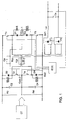
- FIG 1 illustrates the basic architecture of the apparatus according to the invention.
- the conductors of the input line, designated by LI, supply by means of an upstream filter not shown in the figure, the positive and negative bars of the two-stage inverter.
- Each stage comprises two semiconductor switches l1, l2 - l3, l4 and two recirculation diodes D1, D2 - D3, D4.
- the two capacitors C2 and C4 are connected in parallel to the string Str 2 of two switches and two diodes, characterized in that the two switches l2 and l4 have a common point; the capacitors are in turn connected in series and their central point is connected to the central point of the string of switches and diodes Com 2: therefore, more accurately, to the common point of the two switches.
- the central point Com 1 of the string Str 1 of two switches and two diodes is connected to the central point of the string Str 2 of two switches and two diodes - and therefore also to the central point of the series of two capacitors cited above - across a coupling capacitor C2, with a corresponding discharge resistor Rsc.
- the corresponding snubbers Sn1 ⁇ Sn4 are connected in parallel to the four diodes D1 ⁇ D4.
- One of the two primary windings of the isolating transformer is connected in the common points between each semiconductor switch and the corresponding recirculation diode, which individually belongs to each one of the two stages.
- a winding of the current transducer TDI is connected in series to each primary winding, and monitors the current in the two primary windings of the transformer.
- the signal provided by the transducer is processed by the control logic of the inverter, which corrects the duration of the power-on sequences of the semiconductor switches, in order to ensure the best balancing of the conduction steps of the two stages that constitute the power supply apparatus and avoid the formation of a continuous component in the primary winding of the main transformer.
- Two secondary windings supply two single-phase bridges (P1, P2), which supply power to the users by means of a filter Lu, Cu.
- the users can be classic static converters (suitable for DC to AC conversion or for DC to DC conversion), which in turn supply the loads, or can be directly constituted by the final loads.
- An electronic driving and control system manages the correct operation of the power supply apparatus.
- the connections of the two stages that constitute the power supply apparatus can be carried to a terminal strip having no more than 9 terminals, which constitutes a voltage changer (CT).
- CT voltage changer
- the machine can be preset to be series-connected or parallel-connected and to receive the full input voltage or half of it, by means of the connection of the terminals in three sets only.
- the nominal power can be delivered by the machine, in both cases, with an equal stress affecting the components of the converter.
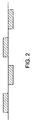
- Figure 2 shows the output voltage at the transformer, which in the specific case is obtained with a particular adjustment technique known as phase shifting, which is adapted to control the delivered voltage and/or current according to the requirements of the users.
- phase shifting a particular adjustment technique known as phase shifting, which is adapted to control the delivered voltage and/or current according to the requirements of the users.
- the switch-on angle of l2, l4 with respect to l1, l3 varies, the voltage applied to the main transformer varies and the output voltage is thus adjusted.
- Other adjustment methods can be used likewise.
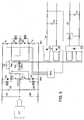
- Figure 3 illustrates an apparatus according to a further aspect of the invention, and further comprising two tertiary low voltage windings, a corresponding rectifier bridge P3, a regulator REG, and an output filter Lb, Cb.
- the power supply apparatus shown in the embodiment of Figure 3 can be used, typically but not exclusively, for charging one or more batteries which are usually present in the more characteristic applications of power supply apparatus such as the one to which the present invention relates.
- This second output of the power supply apparatus is completed by a system for detecting the delivery parameters and by its own regulation system (REG), generally of the switching type, which are designed to correctly manage the voltage and current values supplied to the battery and to the corresponding users.
- REG own regulation system
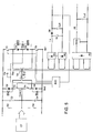
- the apparatus further comprises a solid-state switch T5 / D5, acting as a step-up converter, which is driven, when active, by the control logic synchronously with the solid-state switches T1 ⁇ T4.
- this apparatus allows to optimize the sizing of the four solid-state switches of the converter with respect to switching losses. These losses constitute the largest fraction of all operating losses of these semiconductors in the classic applications of this type of machine.
Abstract
Description
- The present invention relates to an inverter-type power supply apparatus operating at high frequencies, comprising two series-connected input stages, which are connected to a single isolating transformer, and an electronic driving and control circuit.
- In particular, the invention relates to an apparatus for supplying power by static conversion of energy of the above described type, adapted to supply high-power users, with a regulated and/or stabilized output, by drawing energy from high-voltage DC supplies, typically but not exclusively up to 4000 V.
- Power supply systems of this type are generally constituted by H-type bridges, which use multiple semiconductor switches connected in series in the individual bridge branches.
- Alternatively, a circuit solution is used which employs multiple H-type bridges (in a configuration with four semiconductor switches, or with two semiconductor switches plus two switching capacitors) connected in series, each provided with its own isolating transformer, which is required in order to allow correct organization of the connections of the outputs so as to achieve performance at nominal power, and other accessories, such as filters and individual control systems.
- In a further third alternative, converters are used in two cascade-connected stages, each constituted by two switches and two diodes, with a common point at the central point of the supply voltage.
- The above described devices entail problems of various kinds.
- In particular, in the first case the operation of the series-connected semiconductor switches is always delicate and difficult to achieve, owing to the scattering of the characteristic switching parameters of individual components. This fact entails evident optimization problems and additional activities for component selection.
- All this makes it impossible, in case of failure of a component, to replace the component directly without taking specific measures aimed at preserving the correct, safe and reliable functionality of the machine. Accordingly, maintenance is much more complicated and is possible only by replacing simultaneously all the semiconductor components that operate synchronously with a corresponding number of selected components. These requirements often cause malfunctions, since during maintenance the adequate professional expertise is rarely available.
- In the second case, the need to provide functionally autonomous modules, each including a complete H-type bridge and its controls, with the corresponding isolating transformer, makes the machine very complicated, bulky and heavy. Already in the case of a power supply provided at a relatively high voltage, for example 4000 V, it is necessary to connect in series multiple complete functional units connected in an H-type bridge configuration so that each unit is subjected to an input voltage which is compatible with the characteristics of the semiconductor switches that are used. It is also necessary to solve, by means of appropriate HW and SW provisions, the problem of correct balancing of the voltages in input to the various H-type bridges.
- In the case of the third cited alternative, there are significant constraints in the criteria for sizing the transformer and the snubbers: in particular, it is necessary to minimize leakage reactance between the two primary windings (for example by means of a two-wire winding, generally suitable only for low input voltages; whereas in the typical applications of this converter the supply voltages - and therefore the isolation voltages between the primary windings - are on the order of a few thousand volts) in order to avoid the circulation of long-duration current waves in the recirculation diodes as a consequence of the discharge of the energy stored in the inductor. This phenomenon, which is even more critical where capacitive snubbers are provided, can lead to the destruction of the diodes.
- These basic problems and others, particularly those related to the number of semiconductor switches used for each module, are overcome and solved by a power supply apparatus comprising an inverter circuit with two series-connected stages, complete with control and monitoring device, characterized in that:
- each stage comprises only two semiconductor switches and two recirculation diodes; the central point of each one of the two strings of two switches and two diodes being connected to the central point of the second string of two switches and two diodes by means of a coupling capacitor and the corresponding discharge resistor;
- two main line capacitors, in series to each other, being connected to the string of switches and diodes, the two switches having a common point, which is in turn connected to the common point of the two capacitors;
- a connection to a primary winding of the isolating transformer being derived from the common point between the semiconductor switch and the diode of one branch and the common point between the semiconductor switch and the recirculation diode of the second branch of the same stage; a connection to the second primary winding of the isolating transformer being derived from the similar common points between the semiconductor switches and the diodes of the second stage;
- a connection between the semiconductor groups and the two primary windings of the transformer comprising a current transducer, which monitors the current in the two primary windings of the isolating transformer, and by the action of the control and monitoring system prevents the formation of a continuous component in the primary windings of the main transformer;
- a single transformer being necessary and sufficient to adapt the output parameters and ensure full insulation between the input and the output of the apparatus; the leakage reactance between the two primary windings being as high as necessary, in order to allow the system to operate correctly and safely, even in the case of considerable input voltages;
- the great leakage reactance between the two primary windings of the main transformer furthermore allows the use of snubbers of any kind, since they are decoupled by said reactance; accordingly, correct and fast inversion of the charge of the capacitor of the snubber being achieved without producing excessive current phenomena regarding the sizing of the components involved;
- two secondary windings of the isolating transformer supplying a corresponding number of rectifier bridges, which supply, by means of an optional filter, energy to the users, typically inverters suitable to supply the final loads at industrial frequency;
- four semiconductor switches being affected, in normal operating conditions, as regards the locking voltage, for half the input voltage of the apparatus, minus the usual safety factor; the current sizing of said semiconductor switches being obtained from the ratio between nominal machine power rating and half of the voltage in input to the system;
- in normal operating conditions, at least two semiconductor switches being always in the off condition, when the other two are on; over 360° of the period, one or the other of the two stages that constitute the system being in locked condition;
- when the machine is in inactive conditions, with the four semiconductor switches in locked condition, the overall impulse voltage of the two stages in series being twice the input voltage of the apparatus, plus the usual safety factor used in sizing the individual semiconductor switches; for example, the impulse voltage being equal to 13200 V, with a voltage in input to the system of 4000V.
-
- The invention will be now described with reference to the accompanying drawings, given merely by way of non-limitative example, wherein:
- Figure 1 is a circuit diagram of a power supply apparatus according to the invention;
- Figure 2 plots the waveform of the voltage at the transformer;
- Figure 3 shows a circuit diagram of a power supply apparatus according to a further aspect of the invention;
- Figure 4 illustrates a variant of the machine architecture of Figure 1, in which a solid-state switch T5 and a diode D5 are inserted on the output circuit of the machine, downstream of Lu.
- Figure 5 illustrates a variant of the machine architecture of Figure 3, in which a solid-state switch T5 and a diode D5 are inserted on the circuit of the main output of the machine, downstream of Lu.
-
- Figure 1 illustrates the basic architecture of the apparatus according to the invention.
- The conductors of the input line, designated by LI, supply, by means of an upstream filter not shown in the figure, the positive and negative bars of the two-stage inverter.
- Each stage comprises two semiconductor switches l1, l2 - l3, l4 and two recirculation diodes D1, D2 - D3, D4.
- The two capacitors C2 and C4 are connected in parallel to the
string Str 2 of two switches and two diodes, characterized in that the two switches l2 and l4 have a common point; the capacitors are in turn connected in series and their central point is connected to the central point of the string of switches and diodes Com 2: therefore, more accurately, to the common point of the two switches. - The
central point Com 1 of thestring Str 1 of two switches and two diodes is connected to the central point of thestring Str 2 of two switches and two diodes - and therefore also to the central point of the series of two capacitors cited above - across a coupling capacitor C2, with a corresponding discharge resistor Rsc. - The corresponding snubbers Sn1÷Sn4 are connected in parallel to the four diodes D1÷D4.
- One of the two primary windings of the isolating transformer is connected in the common points between each semiconductor switch and the corresponding recirculation diode, which individually belongs to each one of the two stages.
- A winding of the current transducer TDI is connected in series to each primary winding, and monitors the current in the two primary windings of the transformer. The signal provided by the transducer is processed by the control logic of the inverter, which corrects the duration of the power-on sequences of the semiconductor switches, in order to ensure the best balancing of the conduction steps of the two stages that constitute the power supply apparatus and avoid the formation of a continuous component in the primary winding of the main transformer.
- Two secondary windings supply two single-phase bridges (P1, P2), which supply power to the users by means of a filter Lu, Cu. The users can be classic static converters (suitable for DC to AC conversion or for DC to DC conversion), which in turn supply the loads, or can be directly constituted by the final loads.
- An electronic driving and control system (ECC) manages the correct operation of the power supply apparatus.
- The connections of the two stages that constitute the power supply apparatus can be carried to a terminal strip having no more than 9 terminals, which constitutes a voltage changer (CT). Accordingly, as an option, the machine can be preset to be series-connected or parallel-connected and to receive the full input voltage or half of it, by means of the connection of the terminals in three sets only. The nominal power can be delivered by the machine, in both cases, with an equal stress affecting the components of the converter.
- Figure 2 shows the output voltage at the transformer, which in the specific case is obtained with a particular adjustment technique known as phase shifting, which is adapted to control the delivered voltage and/or current according to the requirements of the users. As the switch-on angle of l2, l4 with respect to l1, l3 varies, the voltage applied to the main transformer varies and the output voltage is thus adjusted. Other adjustment methods can be used likewise.
- Figure 3 illustrates an apparatus according to a further aspect of the invention, and further comprising two tertiary low voltage windings, a corresponding rectifier bridge P3, a regulator REG, and an output filter Lb, Cb.
- This architecture is provided by way of non-limitative example of the possible solutions that can be provided for output parameter adjustment. Other circuit solutions are possible in full compliance with the particular features related to the functionality of the basic layout to which the invention relates. The power supply apparatus shown in the embodiment of Figure 3 can be used, typically but not exclusively, for charging one or more batteries which are usually present in the more characteristic applications of power supply apparatus such as the one to which the present invention relates.
- This second output of the power supply apparatus according to the invention is completed by a system for detecting the delivery parameters and by its own regulation system (REG), generally of the switching type, which are designed to correctly manage the voltage and current values supplied to the battery and to the corresponding users.
- The two embodiments of the apparatus, shown in Figures 4 and 5 will be described only once and together, since their structure and operating principle are substantially similar.
- According to this aspect of the invention, the apparatus further comprises a solid-state switch T5 / D5, acting as a step-up converter, which is driven, when active, by the control logic synchronously with the solid-state switches T1÷T4.
- Whenever the variation range of the voltage in input to the converter is sufficiently wide, typically but not exclusively wider than a 1:2 ratio, this apparatus allows to optimize the sizing of the four solid-state switches of the converter with respect to switching losses. These losses constitute the largest fraction of all operating losses of these semiconductors in the classic applications of this type of machine.
- The wider the variation range of the input voltage beyond the typical twofold value, the more it becomes important to contain the switching losses of solid-state switches.
- Bearing in mind that switching losses are, minus second-order factors, proportional to the product of the maximum voltage to be switched and the maximum switching current involved, at the operating frequency of the machine, it is assumed, in accordance with the assumption of functionality on which this variant is based, that the output control covers, by virtue of the phase adjustment of the four solid-state switches, a preset portion of the variation range of the input voltage starting from its maximum value.
- With such assumption, when the input voltage reaches a value equal to the preset value of the above mentioned adjustment range, the converter reaches the full-conduction condition, with half-waves of 180° each. At this point, if the input voltage drops again, adjustment of the step-up type, which can be obtained with appropriate criteria for controlling and monitoring the solid-state switch T5, is activated. This adjustment is active in the variation range of the input voltage from the preset value to the minimum allowed value of the voltage, while the main converter operates in a condition with 180° of conduction for each half-wave.
- If, for example, the variation range of the input voltage varies in the range of 1 to 4, and if the output voltage is controlled with the assumption of:
- a) covering half of the range with phase-adjustment operation of the four switches that constitute the converter,
- b) covering the other half by means of the action of the step-up unit, while the converter operates with full conduction of 180° for each half-wave, the switching losses of the solid-state switches of the converter are halved.
-
- The above indications are given by way of example. Depending on convenience and without limitations or prejudice of any kind, it is possible to choose wider input voltage variation ranges and ratios other than 1:1 for the intervention of phase adjustment with respect to activation of the step-up regulator.
Claims (9)
- A power supply apparatus comprising an inverter circuit with two series-connected stages, complete with control and monitoring device, characterized in that:each stage comprises only two semiconductor switches and two recirculation diodes; the central point of each one of the two strings of two switches and two diodes being connected to the central point of the second string of two switches and two diodes by means of a coupling capacitor and the corresponding discharge resistor;two main line capacitors, in series to each other, being connected to the string of switches and diodes, the two switches having a common point, which is in turn connected to the common point of the two capacitors;a connection to a primary winding of the isolating transformer being derived from the common point between the semiconductor switch and the diode of one branch and the common point between the semiconductor switch and the recirculation diode of the second branch of the same stage; a connection to the second primary winding of the isolating transformer being derived from the similar common points between the semiconductor switches and the diodes of the second stage;a connection between the semiconductor groups and the two primary windings of the transformer comprising a current transducer, which monitors the current in the two primary windings of the isolating transformer, and by the action of the control and monitoring system prevents the formation of a continuous component in the primary windings of the main transformer;a single transformer adapting the output parameters and ensuring full insulation between the input and the output of the apparatus;two secondary windings of the isolating transformer supplying a corresponding number of rectifier bridges, which supply, by means of an optional filter, energy to the users,four semiconductor switches being affected, in normal operating conditions, as regards the locking voltage, for half the input voltage of the apparatus, minus the usual safety factor; the current sizing of said semiconductor switches being obtained from the ratio between nominal machine power rating and half of the voltage in input to the apparatus;in normal operating conditions, at least two semiconductor switches being always in the off condition, when the other two are on; over 360° of the period, one or the other of the two stages that constitute the apparatus being in locked condition;when the machine is in inactive conditions, with the four semiconductor switches in locked condition, the overall impulse voltage of the two stages in series being twice the input voltage of the apparatus, plus the usual safety factor used in sizing the individual semiconductor switches.
- The power supply apparatus according to claim 1, wherein downstream of the DC output stage an adjustment module of the step-up type is added for limiting the extent of the intervention range of the phase adjustment system that acts on the solid-state switches of the converter.
- The power supply apparatus according to claim 1, wherein the semiconductor switches are IGBTs (insulated gate bipolar transistors).
- The power supply apparatus according to claim 1, wherein the semiconductor switches are GTOs (gate turn-off thyristors).
- The power supply apparatus according to one or more of the preceding claims, wherein the transformer comprises a double tertiary winding with a rectified and regulated low-voltage output, used to charge one or more service batteries.
- The power supply apparatus according to claim 5, further comprising additional pairs of secondary windings, suitable to supply differentiated users.
- The power supply apparatus according to one or more of the preceding claims, wherein at least part of the terminals are carried to a voltage changer in order to allow the power supply apparatus to receive an input at full voltage, or half thereof, delivering in both cases the full nominal power to the users, with equal stresses affecting the components of the machine.
- The power supply apparatus according to one or more of the preceding claims, only comprising two input stages and two low-voltage output rectifiers, suitable to supply a battery placed as a buffer to the users, or any other direct DC user, including motors, used for example for the propulsion of any machine, wherein the control and monitoring circuits directly switch on the semiconductor switches with appropriate sequences, in order to adjust the voltage / current / torque / rpm rate supplied to the users.
- A power supply apparatus constituted by multiple apparatuses according to one or more of the preceding claims, which are series-connected in order to allow to supply power to the users when the input voltage is a whole or fractional multiple of the maximum allowable voltage for a single two-stage system comprising four semiconductor switches.
Applications Claiming Priority (2)
| Application Number | Priority Date | Filing Date | Title |
|---|---|---|---|
| ITGE010016 | 2001-02-23 | ||
| IT2001GE000016A ITGE20010016A1 (en) | 2001-02-23 | 2001-02-23 | POWER SUPPLY SYSTEM INCLUDING A HALF-DOUBLE BRIDGE CONVERTER. |
Publications (3)
| Publication Number | Publication Date |
|---|---|
| EP1246352A2 true EP1246352A2 (en) | 2002-10-02 |
| EP1246352A3 EP1246352A3 (en) | 2004-06-30 |
| EP1246352B1 EP1246352B1 (en) | 2009-06-24 |
Family
ID=11442734
Family Applications (1)
| Application Number | Title | Priority Date | Filing Date |
|---|---|---|---|
| EP02003976A Expired - Lifetime EP1246352B1 (en) | 2001-02-23 | 2002-02-22 | Inverter-type power supply apparatus |
Country Status (5)
| Country | Link |
|---|---|
| EP (1) | EP1246352B1 (en) |
| AT (1) | ATE434857T1 (en) |
| DE (1) | DE60232698D1 (en) |
| ES (1) | ES2328672T3 (en) |
| IT (1) | ITGE20010016A1 (en) |
Citations (5)
| Publication number | Priority date | Publication date | Assignee | Title |
|---|---|---|---|---|
| US4754385A (en) * | 1987-01-30 | 1988-06-28 | Varo, Inc. | Two transistor flyback switching converter with current sensing for discontinuous operation |
| EP0483897A1 (en) * | 1990-10-24 | 1992-05-06 | Telefonaktiebolaget L M Ericsson | A method and circuit arrangement for outbalancing input and/or output voltage deviations in converters |
| US5180964A (en) * | 1990-03-28 | 1993-01-19 | Ewing Gerald D | Zero-voltage switched FM-PWM converter |
| US5781419A (en) * | 1996-04-12 | 1998-07-14 | Soft Switching Technologies, Inc. | Soft switching DC-to-DC converter with coupled inductors |
| WO1998042065A1 (en) * | 1997-03-14 | 1998-09-24 | Italtel S.P.A. | High power dc/dc converter |
-
2001
- 2001-02-23 IT IT2001GE000016A patent/ITGE20010016A1/en unknown
-
2002
- 2002-02-22 AT AT02003976T patent/ATE434857T1/en not_active IP Right Cessation
- 2002-02-22 ES ES02003976T patent/ES2328672T3/en not_active Expired - Lifetime
- 2002-02-22 EP EP02003976A patent/EP1246352B1/en not_active Expired - Lifetime
- 2002-02-22 DE DE60232698T patent/DE60232698D1/en not_active Expired - Lifetime
Patent Citations (5)
| Publication number | Priority date | Publication date | Assignee | Title |
|---|---|---|---|---|
| US4754385A (en) * | 1987-01-30 | 1988-06-28 | Varo, Inc. | Two transistor flyback switching converter with current sensing for discontinuous operation |
| US5180964A (en) * | 1990-03-28 | 1993-01-19 | Ewing Gerald D | Zero-voltage switched FM-PWM converter |
| EP0483897A1 (en) * | 1990-10-24 | 1992-05-06 | Telefonaktiebolaget L M Ericsson | A method and circuit arrangement for outbalancing input and/or output voltage deviations in converters |
| US5781419A (en) * | 1996-04-12 | 1998-07-14 | Soft Switching Technologies, Inc. | Soft switching DC-to-DC converter with coupled inductors |
| WO1998042065A1 (en) * | 1997-03-14 | 1998-09-24 | Italtel S.P.A. | High power dc/dc converter |
Non-Patent Citations (2)
| Title |
|---|
| DEMERCIL S. OLIVEIRA ET AL.: 'A lossless commutation PWM two level forward converter.' IEEE 10 September 2000, pages 582 - 588, XP000968742 * |
| 'Dual voltage clamp circuit.' IBM TECHNICAL DISCLOSURE BULLETIN vol. 32, no. 2, July 1989, NEW YORK, pages 172 - 173, XP000033388 * |
Also Published As
| Publication number | Publication date |
|---|---|
| ITGE20010016A1 (en) | 2002-08-23 |
| ES2328672T3 (en) | 2009-11-17 |
| EP1246352B1 (en) | 2009-06-24 |
| EP1246352A3 (en) | 2004-06-30 |
| ATE434857T1 (en) | 2009-07-15 |
| DE60232698D1 (en) | 2009-08-06 |
Similar Documents
| Publication | Publication Date | Title |
|---|---|---|
| US8138694B2 (en) | Bidirectional buck-boost power converters | |
| US7394668B2 (en) | Switching power supply circuit and frequency converter | |
| JP2680494B2 (en) | Single-phase AC power converter | |
| JP5425193B2 (en) | Circuit configuration with power input and operation method for controlling power input circuit | |
| AU2007202910B2 (en) | Power supply for electrostatic precipitator | |
| US7622825B2 (en) | Wide-voltage-range converter | |
| EP3455934B1 (en) | Regulating transformer rectifier unit for dc power applications | |
| US20070228837A1 (en) | Apparatus for and methods of polyphase power conversion | |
| US20170237355A1 (en) | Dc-to-dc converter comprising a transformer | |
| US9479011B2 (en) | Method and system for a dual conversion uninterruptible power supply | |
| US11967859B2 (en) | Power factor correction circuit, power factor correction assembly and on-line uninterruptible power supply comprising same | |
| US20170310111A1 (en) | High voltage dc power supply for high power radio frequency amplifiers | |
| KR101768256B1 (en) | Inverter with power cell of dual structure | |
| EP1246352B1 (en) | Inverter-type power supply apparatus | |
| US10158284B2 (en) | PFC with stacked half-bridges on DC side of rectifier | |
| EP3211783B1 (en) | Multiple output rectifier | |
| JPH07284271A (en) | Switching power supply apparatus | |
| US20230352930A1 (en) | Dc power distribution system | |
| KR100490645B1 (en) | Uninterruptible power supply of non-insulation | |
| WO2023172627A1 (en) | Solid-state power controller with transformer soft-start | |
| JPH04275022A (en) | Method of starting dc power supply system | |
| JP2000092709A (en) | Active filter device | |
| Séguier et al. | Introduction and Presentation | |
| KR20040087103A (en) | Automatically liner conditioner using a multifunctional filter and a ac voltage controller |
Legal Events
| Date | Code | Title | Description |
|---|---|---|---|
| PUAI | Public reference made under article 153(3) epc to a published international application that has entered the european phase |
Free format text: ORIGINAL CODE: 0009012 |
|
| AK | Designated contracting states |
Kind code of ref document: A2 Designated state(s): AT BE CH CY DE DK ES FI FR GB GR IE IT LI LU MC NL PT SE TR |
|
| AX | Request for extension of the european patent |
Free format text: AL;LT;LV;MK;RO;SI |
|
| PUAL | Search report despatched |
Free format text: ORIGINAL CODE: 0009013 |
|
| AK | Designated contracting states |
Kind code of ref document: A3 Designated state(s): AT BE CH CY DE DK ES FI FR GB GR IE IT LI LU MC NL PT SE TR |
|
| AX | Request for extension of the european patent |
Extension state: AL LT LV MK RO SI |
|
| 17P | Request for examination filed |
Effective date: 20041116 |
|
| AKX | Designation fees paid |
Designated state(s): AT BE CH CY DE DK ES FI FR GB GR IE IT LI LU MC NL PT SE TR |
|
| RAP1 | Party data changed (applicant data changed or rights of an application transferred) |
Owner name: R.G.M. S.P.A. |
|
| GRAP | Despatch of communication of intention to grant a patent |
Free format text: ORIGINAL CODE: EPIDOSNIGR1 |
|
| GRAS | Grant fee paid |
Free format text: ORIGINAL CODE: EPIDOSNIGR3 |
|
| GRAA | (expected) grant |
Free format text: ORIGINAL CODE: 0009210 |
|
| AK | Designated contracting states |
Kind code of ref document: B1 Designated state(s): AT BE CH CY DE DK ES FI FR GB GR IE IT LI LU MC NL PT SE TR |
|
| REG | Reference to a national code |
Ref country code: GB Ref legal event code: FG4D |
|
| REG | Reference to a national code |
Ref country code: CH Ref legal event code: EP |
|
| REG | Reference to a national code |
Ref country code: IE Ref legal event code: FG4D |
|
| REF | Corresponds to: |
Ref document number: 60232698 Country of ref document: DE Date of ref document: 20090806 Kind code of ref document: P |
|
| PG25 | Lapsed in a contracting state [announced via postgrant information from national office to epo] |
Ref country code: AT Free format text: LAPSE BECAUSE OF FAILURE TO SUBMIT A TRANSLATION OF THE DESCRIPTION OR TO PAY THE FEE WITHIN THE PRESCRIBED TIME-LIMIT Effective date: 20090624 Ref country code: FI Free format text: LAPSE BECAUSE OF FAILURE TO SUBMIT A TRANSLATION OF THE DESCRIPTION OR TO PAY THE FEE WITHIN THE PRESCRIBED TIME-LIMIT Effective date: 20090624 |
|
| REG | Reference to a national code |
Ref country code: ES Ref legal event code: FG2A Ref document number: 2328672 Country of ref document: ES Kind code of ref document: T3 |
|
| PG25 | Lapsed in a contracting state [announced via postgrant information from national office to epo] |
Ref country code: SE Free format text: LAPSE BECAUSE OF FAILURE TO SUBMIT A TRANSLATION OF THE DESCRIPTION OR TO PAY THE FEE WITHIN THE PRESCRIBED TIME-LIMIT Effective date: 20090924 |
|
| NLV1 | Nl: lapsed or annulled due to failure to fulfill the requirements of art. 29p and 29m of the patents act | ||
| PG25 | Lapsed in a contracting state [announced via postgrant information from national office to epo] |
Ref country code: NL Free format text: LAPSE BECAUSE OF FAILURE TO SUBMIT A TRANSLATION OF THE DESCRIPTION OR TO PAY THE FEE WITHIN THE PRESCRIBED TIME-LIMIT Effective date: 20090624 Ref country code: BE Free format text: LAPSE BECAUSE OF FAILURE TO SUBMIT A TRANSLATION OF THE DESCRIPTION OR TO PAY THE FEE WITHIN THE PRESCRIBED TIME-LIMIT Effective date: 20090624 |
|
| PG25 | Lapsed in a contracting state [announced via postgrant information from national office to epo] |
Ref country code: PT Free format text: LAPSE BECAUSE OF FAILURE TO SUBMIT A TRANSLATION OF THE DESCRIPTION OR TO PAY THE FEE WITHIN THE PRESCRIBED TIME-LIMIT Effective date: 20091024 |
|
| PG25 | Lapsed in a contracting state [announced via postgrant information from national office to epo] |
Ref country code: DK Free format text: LAPSE BECAUSE OF FAILURE TO SUBMIT A TRANSLATION OF THE DESCRIPTION OR TO PAY THE FEE WITHIN THE PRESCRIBED TIME-LIMIT Effective date: 20090624 |
|
| PLBE | No opposition filed within time limit |
Free format text: ORIGINAL CODE: 0009261 |
|
| STAA | Information on the status of an ep patent application or granted ep patent |
Free format text: STATUS: NO OPPOSITION FILED WITHIN TIME LIMIT |
|
| 26N | No opposition filed |
Effective date: 20100325 |
|
| REG | Reference to a national code |
Ref country code: CH Ref legal event code: PL |
|
| GBPC | Gb: european patent ceased through non-payment of renewal fee |
Effective date: 20100222 |
|
| PG25 | Lapsed in a contracting state [announced via postgrant information from national office to epo] |
Ref country code: GR Free format text: LAPSE BECAUSE OF FAILURE TO SUBMIT A TRANSLATION OF THE DESCRIPTION OR TO PAY THE FEE WITHIN THE PRESCRIBED TIME-LIMIT Effective date: 20090925 Ref country code: LI Free format text: LAPSE BECAUSE OF NON-PAYMENT OF DUE FEES Effective date: 20100228 Ref country code: MC Free format text: LAPSE BECAUSE OF NON-PAYMENT OF DUE FEES Effective date: 20100301 Ref country code: CH Free format text: LAPSE BECAUSE OF NON-PAYMENT OF DUE FEES Effective date: 20100228 |
|
| PG25 | Lapsed in a contracting state [announced via postgrant information from national office to epo] |
Ref country code: IE Free format text: LAPSE BECAUSE OF NON-PAYMENT OF DUE FEES Effective date: 20100222 |
|
| PG25 | Lapsed in a contracting state [announced via postgrant information from national office to epo] |
Ref country code: GB Free format text: LAPSE BECAUSE OF NON-PAYMENT OF DUE FEES Effective date: 20100222 |
|
| PG25 | Lapsed in a contracting state [announced via postgrant information from national office to epo] |
Ref country code: CY Free format text: LAPSE BECAUSE OF FAILURE TO SUBMIT A TRANSLATION OF THE DESCRIPTION OR TO PAY THE FEE WITHIN THE PRESCRIBED TIME-LIMIT Effective date: 20090624 |
|
| PG25 | Lapsed in a contracting state [announced via postgrant information from national office to epo] |
Ref country code: LU Free format text: LAPSE BECAUSE OF NON-PAYMENT OF DUE FEES Effective date: 20100222 |
|
| PG25 | Lapsed in a contracting state [announced via postgrant information from national office to epo] |
Ref country code: TR Free format text: LAPSE BECAUSE OF FAILURE TO SUBMIT A TRANSLATION OF THE DESCRIPTION OR TO PAY THE FEE WITHIN THE PRESCRIBED TIME-LIMIT Effective date: 20090624 |
|
| REG | Reference to a national code |
Ref country code: FR Ref legal event code: PLFP Year of fee payment: 15 |
|
| REG | Reference to a national code |
Ref country code: FR Ref legal event code: PLFP Year of fee payment: 16 |
|
| REG | Reference to a national code |
Ref country code: FR Ref legal event code: PLFP Year of fee payment: 17 |
|
| REG | Reference to a national code |
Ref country code: DE Ref legal event code: R082 Ref document number: 60232698 Country of ref document: DE Representative=s name: MAUCHER JENKINS PATENTANWAELTE & RECHTSANWAELT, DE Ref country code: DE Ref legal event code: R081 Ref document number: 60232698 Country of ref document: DE Owner name: ABB SCHWEIZ AG, CH Free format text: FORMER OWNER: R.G.M. S.P.A., GENUA/GENOVA, IT |
|
| REG | Reference to a national code |
Ref country code: ES Ref legal event code: PC2A Owner name: ABB SCHWEIZ AG Effective date: 20200605 |
|
| PGFP | Annual fee paid to national office [announced via postgrant information from national office to epo] |
Ref country code: FR Payment date: 20210224 Year of fee payment: 20 Ref country code: IT Payment date: 20210222 Year of fee payment: 20 |
|
| PGFP | Annual fee paid to national office [announced via postgrant information from national office to epo] |
Ref country code: DE Payment date: 20210217 Year of fee payment: 20 |
|
| PGFP | Annual fee paid to national office [announced via postgrant information from national office to epo] |
Ref country code: ES Payment date: 20210421 Year of fee payment: 20 |
|
| REG | Reference to a national code |
Ref country code: DE Ref legal event code: R071 Ref document number: 60232698 Country of ref document: DE |
|
| PG25 | Lapsed in a contracting state [announced via postgrant information from national office to epo] |
Ref country code: ES Free format text: LAPSE BECAUSE OF EXPIRATION OF PROTECTION Effective date: 20220223 |