EP1237268A2 - Voltage converter - Google Patents
Voltage converter Download PDFInfo
- Publication number
- EP1237268A2 EP1237268A2 EP01130956A EP01130956A EP1237268A2 EP 1237268 A2 EP1237268 A2 EP 1237268A2 EP 01130956 A EP01130956 A EP 01130956A EP 01130956 A EP01130956 A EP 01130956A EP 1237268 A2 EP1237268 A2 EP 1237268A2
- Authority
- EP
- European Patent Office
- Prior art keywords
- voltage
- voltage converter
- rectifier
- active switching
- capacitor
- Prior art date
- Legal status (The legal status is an assumption and is not a legal conclusion. Google has not performed a legal analysis and makes no representation as to the accuracy of the status listed.)
- Withdrawn
Links
Images
Classifications
-
- H—ELECTRICITY
- H02—GENERATION; CONVERSION OR DISTRIBUTION OF ELECTRIC POWER
- H02M—APPARATUS FOR CONVERSION BETWEEN AC AND AC, BETWEEN AC AND DC, OR BETWEEN DC AND DC, AND FOR USE WITH MAINS OR SIMILAR POWER SUPPLY SYSTEMS; CONVERSION OF DC OR AC INPUT POWER INTO SURGE OUTPUT POWER; CONTROL OR REGULATION THEREOF
- H02M3/00—Conversion of dc power input into dc power output
- H02M3/22—Conversion of dc power input into dc power output with intermediate conversion into ac
- H02M3/24—Conversion of dc power input into dc power output with intermediate conversion into ac by static converters
- H02M3/28—Conversion of dc power input into dc power output with intermediate conversion into ac by static converters using discharge tubes with control electrode or semiconductor devices with control electrode to produce the intermediate ac
- H02M3/325—Conversion of dc power input into dc power output with intermediate conversion into ac by static converters using discharge tubes with control electrode or semiconductor devices with control electrode to produce the intermediate ac using devices of a triode or a transistor type requiring continuous application of a control signal
- H02M3/335—Conversion of dc power input into dc power output with intermediate conversion into ac by static converters using discharge tubes with control electrode or semiconductor devices with control electrode to produce the intermediate ac using devices of a triode or a transistor type requiring continuous application of a control signal using semiconductor devices only
- H02M3/33569—Conversion of dc power input into dc power output with intermediate conversion into ac by static converters using discharge tubes with control electrode or semiconductor devices with control electrode to produce the intermediate ac using devices of a triode or a transistor type requiring continuous application of a control signal using semiconductor devices only having several active switching elements
- H02M3/33576—Conversion of dc power input into dc power output with intermediate conversion into ac by static converters using discharge tubes with control electrode or semiconductor devices with control electrode to produce the intermediate ac using devices of a triode or a transistor type requiring continuous application of a control signal using semiconductor devices only having several active switching elements having at least one active switching element at the secondary side of an isolation transformer
- H02M3/33592—Conversion of dc power input into dc power output with intermediate conversion into ac by static converters using discharge tubes with control electrode or semiconductor devices with control electrode to produce the intermediate ac using devices of a triode or a transistor type requiring continuous application of a control signal using semiconductor devices only having several active switching elements having at least one active switching element at the secondary side of an isolation transformer having a synchronous rectifier circuit or a synchronous freewheeling circuit at the secondary side of an isolation transformer
-
- Y—GENERAL TAGGING OF NEW TECHNOLOGICAL DEVELOPMENTS; GENERAL TAGGING OF CROSS-SECTIONAL TECHNOLOGIES SPANNING OVER SEVERAL SECTIONS OF THE IPC; TECHNICAL SUBJECTS COVERED BY FORMER USPC CROSS-REFERENCE ART COLLECTIONS [XRACs] AND DIGESTS
- Y02—TECHNOLOGIES OR APPLICATIONS FOR MITIGATION OR ADAPTATION AGAINST CLIMATE CHANGE
- Y02B—CLIMATE CHANGE MITIGATION TECHNOLOGIES RELATED TO BUILDINGS, e.g. HOUSING, HOUSE APPLIANCES OR RELATED END-USER APPLICATIONS
- Y02B70/00—Technologies for an efficient end-user side electric power management and consumption
- Y02B70/10—Technologies improving the efficiency by using switched-mode power supplies [SMPS], i.e. efficient power electronics conversion e.g. power factor correction or reduction of losses in power supplies or efficient standby modes
Abstract
Description
Die vorliegende Erfindung betrifft einen Spannungskonverter vom Flusswandlertyp nach dem Oberbegriff des Patentanspruchs 1.The present invention relates to a voltage converter of the river converter type according to the preamble of the claim 1.
Derartige Spannungskonverter weisen sekundärseitig einen Synchrongleichrichter auf, welcher zum Erreichen eines möglichst günstigen Wirkungsgrades typischerweise mit MOSFETs realisiert wird. Aus dem Stand der Technik sind zahlreiche Topologien für Flusswandler bekannt, wie etwa Eintakt-, Gegentakt-, Halbbrücken-, Push-Pull-, Vollbrücken- oder Phase-Shift-Flusswandler.Such voltage converters have one on the secondary side Synchronous rectifier, which to achieve one if possible favorable efficiency typically with MOSFETs is realized. There are numerous from the prior art Known topologies for flux converters, such as single-ended, push-pull, Half-bridge, push-pull, full-bridge or phase-shift flux converter.
Insbesondere jedoch das Prinzip der Selbststeuerung von Synchron-Gleichrichtern, nämlich die Verwendung von in der Konverterschaltung selbst bereits vorhandenen bzw. auftretenden Spannungsverläufen zum Ein- bzw. Ausschalten der aktiven Schaltelemente synchron zu primärseitigen Schaltern, kann bei manchen Flusswandler-Topologien, insbesondere solchen, die keine Eintakt-Flusswandler sind, prinzipiell problematisch sein: Wenn bei einem Gegentakt-, Halbbrücken-, Vollbrücken- oder Phase-Shift-Flusswandler primärseitig alle Halbleiter im ausgeschalteten Zustand sind, muss auf der Sekundärseite zu diesem Zeitpunkt der Freilaufstrom durch die aktiven (Gleichrichter-)Schaltelemente geleitet werden, und bei einer Realisierung dieser Elemente durch MOSFETs muss ein entsprechendes Ansteuersignal vorhanden sein. Dieses kann jedoch unmittelbar aus dem Transformator, etwa mittels einer für das Ansteuersignal vorgesehenen Hilfswicklung, nicht ohne weiteres erzeugt werden.In particular, however, the principle of self-regulation by Synchronous rectifiers, namely the use of in the Converter circuit itself already existing or occurring Voltage curves for switching the active on or off Switching elements synchronous to primary switches, with some flux converter topologies, especially those that are not single-ended flow converters, in principle problematic be: If a push-pull, half-bridge, Full-bridge or phase-shift flux converters all on the primary side Semiconductors are switched off, must be on the Secondary side at this time the freewheeling current through the active (rectifier) switching elements are routed, and when these elements are implemented by MOSFETs a corresponding control signal must be available. This can, however, directly from the transformer, for example by means of an auxiliary winding provided for the control signal, are not easily generated.
Aus diesem Grunde ist zwar prinzipiell das Prinzip der Selbststeuerung bekannt, es ist jedoch auf Grund dieser und anderer topologiebedingter Probleme gerade bei Flusswandlern der genannten Topologien nachteilig. For this reason, the principle of Self-control is known, but it is because of this and other topology-related problems, especially with flux converters of the topologies mentioned disadvantageous.
Vielmehr wird bei diesen Flusswandlertopologien (Gegentakt-,
Halbbrücken-, Vollbrücken- oder Phase-Shift-Flusswandlern)
oder anderen Topologien eine Ansteuerung von Leistungshalbleitern
eines sekundärseitigen Synchrongleichrichters,
wie in analoger Weise etwa in dem deutschen Gebrauchsmuster
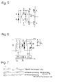
299 01 322 beschrieben, mittels einer Fremdsteuerung
gelöst, wie sie zum Stand der Technik in Fig. 6
schematisch beschrieben ist: Eine PWM-Steuereinheit 10
steuert dabei sowohl eine primärseitige (ansonsten bekannte)
Schalteranordnung selbst, als auch über eine sekundärseitig
von einem Übertrager 16 angeordneten Steuereinheit
14, ein Paar als Synchrongleichrichter wirkender Leistungshalbleiter
18, 20, wobei das Konverter-Ausgangsspannungssignal
über einem Lastwiderstand RL abfällt.Rather, with these flux converter topologies (push-pull, half-bridge, full-bridge or phase-shift flux converters) or other topologies, control of power semiconductors of a secondary-side synchronous rectifier, as described in an analogous manner, for example in German utility model 299 01 322, is achieved by means of an external control 6: A
Die Spannungskurven der Fig. 7 verdeutlichen das Schaltverhalten
der Gleichrichterelemente 18 und 20 relativ zur
Transformatorspannung (erste Kurve), die, bedingt durch die
primärseitige Steuerung, in der gezeigten Weise um die
Nullspannung pendelt: Dagegen besitzen die Ansteuersignale
für die Transistoren 18, 20 (zweite und dritte Kurve) einen
Pegel größer Null zum Aktivieren des jeweiligen Halbleiters
für den Freilaufstrom.The voltage curves in FIG. 7 illustrate the switching behavior
of the
Allerdings ist, wie schon anhand der Fig. 6 deutlich wird, eine derartige Fremdsteuerung der aktiven Schaltelemente des Synchrongleichrichters auf Sekundärseite aufwendig und teuer.However, as is already clear from FIG. 6, such external control of the active switching elements of the synchronous rectifier on the secondary side and complex expensive.
Aufgabe der vorliegenden Erfindung ist es daher, eine Ansteuerung von aktiven Schaltelementen eines Synchrongleichrichters in einem gattungsgemäßen Spannungskonverter der genannten Topologien zu vereinfachen, insbesondere den schaltungstechnischen Aufwand zu verringern, wobei das Prinzip der Selbststeuerung, d. h. Regenerierung der Steuersignale aus bereits in der Konverterschaltung vorhandenen Signalen, ohne die Notwendigkeit externer Signallogiken, eingesetzt werden soll.The object of the present invention is therefore a control of active switching elements of a synchronous rectifier in a generic voltage converter to simplify the topologies mentioned, in particular the to reduce circuit complexity, the Principle of self-control, d. H. Regeneration of the control signals from existing ones in the converter circuit Signals without the need for external signal logic, to be used.
Die Aufgabe wird durch die Vorrichtung mit den Merkmalen des Patentanspruchs 1 gelöst; vorteilhafte Weiterbildungen der Erfindungen sind in den Unteransprüchen beschrieben.The task is accomplished by the device with the features of claim 1 solved; advantageous further training of the inventions are described in the subclaims.
So ist erfindungsgemäß eine Kapazitätsvorrichtung vorgesehen, welche mit ihrer Ladung die Ansteuerenergie (bzw. Ansteuerspannung) für die aktiven Schaltelemente so zwischenspeichert, dass insbesondere auch zu denjenigen Zeitpunkten im Betriebszyklus, zu welchem sekundärseitig an der erfindungsgemäßen Hilfswicklung kein Spannungssignal anliegt, der Ansteuerungsbetrieb und mithin die ordnungsgemäße Funktionsweise des Synchrongleichrichters gewährleistet sein kann.According to the invention, a capacitance device is provided, which with their charge the control energy (or control voltage) cached for the active switching elements that especially at those times in the operating cycle, to which on the secondary side of the invention Auxiliary winding there is no voltage signal, the control mode and therefore the proper functioning of the synchronous rectifier can.
In erfindungsgemäß vorteilhafter Weise wird dabei ausgenutzt, dass das von der Hilfswicklung erzeugte Signal synchron zur Transformatorspannung ist, so dass das Ein- bzw. Ausschalten der aktiven Schaltelemente des Gleichrichters mit hoher Genauigkeit und damit verlustarm erfolgt. Das erfindungsgemäß zur Ansteuerung des Synchrongleichrichters (genauer gesagt: des Steueranschlusses eines betreffenden Gleichrichter-Schaltelements) eingesetzte Halbleiterelement, Diode oder Transistor, ermöglicht dabei in schaltungstechnisch äußerst einfacher Weise die Signalerzeugung und Signalanlegung durch Zusammenwirken von Hilfswicklung und Kapazität.In an advantageous manner according to the invention, use is made of that the signal generated by the auxiliary winding is synchronous to the transformer voltage, so that the input or Switch off the active switching elements of the rectifier done with high accuracy and thus with little loss. The invention to control the synchronous rectifier (more precisely: the control connection of a concerned Rectifier switching element) used semiconductor element, Diode or transistor, allows in circuitry extremely simple way the signal generation and signal application through interaction of auxiliary winding and capacity.
Besonders bevorzugt ist es dabei, einen Kapazitätswert für die Kapazitätsvorrichtung zu wählen, der deutlich höher ist als eine Ansteuerkapazität (z. B. Gatekapazität im Falle eines MOSFET) des Steueranschlusses, so dass die betreffenden Ladungsverhältnisse ein sicheres Ansteuern und stabiles Schalten gewährleisten. Dabei hat sich besonders bewährt, für die Kapazität der Kapazitätsvorrichtung mindestens das fünf- bis zehnfache der für das aktive Schaltelement vorhandenen Ansteuerkapazität zu wählen.It is particularly preferred here to have a capacitance value for to choose the capacity device that is significantly higher as a drive capacity (e.g. gate capacity in the case a MOSFET) of the control connection, so that the relevant Charge conditions a safe control and stable Ensure switching. It has proven particularly useful for the capacity of the capacity device at least that five to ten times that available for the active switching element Select control capacity.
Prinzipiell eignet sich die vorliegende Erfindung für beliebige Topologien auf Primärseite und Sekundärseite; als besonders bevorzugt wären primärseitig Gegentakt-, Vollbrücken-, Halbbrücken- oder Phase-Shift-Topologien, und sekundärseitig Current-Doubler- oder die einfache Mittelpunktkonfiguration mit Speicherdrossel anzusehen.In principle, the present invention is suitable for any Topologies on primary and secondary side; as on the primary side, push-pull, full-bridge, Half-bridge or phase-shift topologies, and on the secondary side Current doubler or simple center configuration view with storage choke.
In einer besonders bevorzugten Ausführungsform der Erfindung ist die Sekundärseite mit zwei Schaltungszweigen als Brückengleichrichter realisiert, so dass für jeden Schaltungszweig ein aktives Schaltelement vorliegt, welches aus einer zugehörigen Hilfswicklung des Paares von Hilfswicklungen mit Ladung bzw. Spannung versorgt wird. Dabei kann es einerseits günstig sein, für beide Zweige einen gemeinsamen Kondensator als Kapazitätsvorrichtung vorzusehen; alternativ sieht eine weitere, bevorzugte Ausführungsform der Erfindung vor, für jeden Zweig eine Reihenschaltung aus Induktivität (d. h. jeweiliger Hilfswicklung) und Kondensator vorzusehen, wobei in diesem Fall das Halbleiterelement als Transistor (besonders bevorzugt: MOSFET) realisiert ist und sein Steuersignal von einem Knoten zwischen Induktivität und Kondensator eines jeweils gegenüberliegenden Zweiges empfängt.In a particularly preferred embodiment of the invention is the secondary side with two circuit branches as Bridge rectifier realized so that for each circuit branch there is an active switching element, which consists of an associated auxiliary winding of the pair of auxiliary windings is supplied with charge or voltage. It can on the one hand it should be favorable for both branches to have a common one Provide a capacitor as a capacitance device; alternative sees another preferred embodiment of the Invention before, a series connection of inductance for each branch (i.e. respective auxiliary winding) and capacitor to provide, in which case the semiconductor element as Transistor (particularly preferred: MOSFET) is realized and its control signal from a node between inductance and capacitor of an opposite branch receives.
Der Vorteil gegenüber einer Ausführungsform mit Dioden als Halbleiterelement bzw. lediglich einem Kondensator liegt darin, dass durch eine solche Schaltung der Kondensator durch die zugehörige Hilfswicklung sowohl aufgeladen, als auch entladen werden und die Steueranschlüsse der aktiven Schaltelemente während der vorgesehenen Ausschaltphasen aktiv auf einen Nullpegel gezogen werden, so dass insbesondere bei schnellen Spannungsänderungen kapazitive Effekte der Leistungshalbleiter selbst nicht zu einem unbeabsichtigten Einschalten führen können. The advantage over an embodiment with diodes as Semiconductor element or only one capacitor in that through such a circuit the capacitor charged by the associated auxiliary winding, as well also be discharged and the control connections of the active Switching elements active during the planned switch-off phases be pulled to a zero level, so in particular capacitive effects with rapid voltage changes the power semiconductor itself does not become an unintended one Switch on can lead.
Eine weitere bevorzugte Ausführungsform der Erfindung liegt darin, die Zweige jeweils mit einem Spannungsbegrenzer zu kombinieren, da die Spannung über einem in jedem Zweig verwendeten Kondensator als Kapazitätselement von der Eingangsspannung des Konverters abhängt und daher, etwa bei großen Eingangsspannungsvariationen, eine maximale Ansteuerspannung am aktiven Schaltelement überschritten werden kann. Zu diesem Zweck bietet es sich besonders an, geeignet angeordnete und angesteuerte MOSFETs kanalseitig zur Spannungsbegrenzung den jeweiligen Steueranschlüssen der aktiven Schaltelemente vorzuschalten.Another preferred embodiment of the invention lies in each of the branches with a voltage limiter combine as the voltage across one used in each branch Capacitor as a capacitance element from the input voltage depends on the converter and therefore, for example at large input voltage variations, a maximum control voltage exceeded on the active switching element can. It is particularly suitable for this purpose arranged and controlled MOSFETs on the channel side Voltage limitation of the respective control connections of the upstream active switching elements.
Im Ergebnis entsteht durch die vorliegende Erfindung in schaltungstechnisch überraschend einfacher Weise ein Spannungskonverter mit selbstgesteuertem Synchrongleichrichter, der sich durch präzises Schaltverhalten der sekundärseitigen Gleichrichterelemente und damit hohe Verlustarmut auszeichnet. Gleichzeitig minimiert die geringe Anzahl der verwendeten Schaltungselemente den herstellungstechnischen Aufwand, so dass insbesondere auch aus fertigungstechnischer Sicht die vorliegende Erfindung große Vorteile aufweist. As a result, the present invention results in In terms of circuit technology, a voltage converter is surprisingly simple with self-controlled synchronous rectifier, which is characterized by the precise switching behavior of the secondary side Rectifier elements and thus low loss. At the same time minimizes the small number of used circuit elements the manufacturing technology Effort, so that in particular also from a manufacturing point of view Point of view, the present invention has great advantages.
Weitere Vorteile, Merkmale und Einzelheiten der Erfindung ergeben sich aus der nachfolgenden Beschreibung bevorzugter Ausführungsbeispiele sowie anhand der Zeichnungen; diese zeigen in
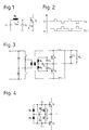
- Fig. 1:
- ein prinzipielles Schaltbild zur Verdeutlichung der Erzeugung eines Ansteuersignals für ein aktives Gleichrichterschaltelement mittels Hilfswicklung und Kondensator;
- Fig. 2:
- ein Signaldiagramm zum Vergleich der Spannung über der Hilfswicklung und der Ansteuerspannung;
- Fig. 3:
- ein Prinzipschaltbild einer ersten Ausführungsform der vorliegenden Erfindung mit zwei sekundärseitigen aktiven Schaltelementen und jeweils zugeordneter Hilfswicklung bei gemeinsamem Kondensator;
- Fig. 4:
- eine Weiterentwicklung des Prinzips der Fig. 3 (lediglich Ausschnitt der Ansteuerung der Leistungshalbleiter) mittels Transistoren als Schaltelementen und für jeden Zweig separatem Kondensator;
- Fig. 5:
- noch eine Weiterentwicklung des Schaltbildes gem. Fig. 4 mit zusätzlich vorgesehenen, als Spannungsbegrenzer geschalteten Transistoren vor den jeweiligen Steueranschlüssen der aktiven Schaltelemente (best mode);
- Fig. 6:
- ein Prinzipschaltbild eines aus dem Stand der Technik bekannten, fremdgesteuerten Spannungskonverters vom Flusswandlertyp und
- Fig. 7:
- ein Signaldiagramm zum Vergleich der verschiedenen, durch zusätzliche Schaltlogik erzeugten Ansteuersignale für die sekundärseitigen aktiven Gleichrichter-Schaltelemente in Fig. 7.
- Fig. 1:
- a basic circuit diagram to illustrate the generation of a control signal for an active rectifier switching element by means of auxiliary winding and capacitor;
- Fig. 2:
- a signal diagram for comparing the voltage across the auxiliary winding and the drive voltage;
- Fig. 3:
- a schematic diagram of a first embodiment of the present invention with two active switching elements on the secondary side and each associated auxiliary winding with a common capacitor;
- Fig. 4:
- a further development of the principle of FIG. 3 (only section of the control of the power semiconductors) by means of transistors as switching elements and a separate capacitor for each branch;
- Fig. 5:
- Another development of the circuit diagram acc. 4 with additionally provided transistors connected as voltage limiters in front of the respective control connections of the active switching elements (best mode);
- Fig. 6:
- a schematic diagram of an externally controlled voltage converter of the flux converter type and known from the prior art
- Fig. 7:
- 7 shows a signal diagram for comparing the different control signals generated by additional switching logic for the active rectifier switching elements on the secondary side in FIG. 7.
Fig. 1 und Fig. 2 verdeutlichen, wie mit Hilfe eines Kondensators C1 als Kapazitätsvorrichtung sowie einer Diode D1 als Halbleiterelement ein vom Transformator mittels einer Hilfswicklung W1 erzeugtes Transformatorspannungssignal UW1 in der Art eines Spannungsverdopplers zum Erzeugen einer Ansteuerspannung UV1 für das Leistungshalbleiterbauelement V1 so angehoben werden kann, dass, von einem hohen (d. h. Einschalt-)Pegel synchron und in ansonsten bekannter Weise das Leistungshalbleiterelement im Gleichrichterbetrieb periodisch ausgeschaltet wird. Die durch die Spannungsverdopplung im Signal UV1 erzeugten Signalspitzen sind für einen Betrieb des Leistungshalbleiters V1 unschädlich. Die Hilfswicklung ist in ansonsten bekannter Weise auf dem (nicht näher erläuterten) Haupttransformator angebracht und weist eine enge Kopplung mit dessen Leistungswicklungen auf.Fig. 1 and Fig. 2 illustrate how with the help of a capacitor C 1 as a capacitance device and a diode D 1 as a semiconductor element, a transformer voltage signal U W1 generated by the transformer by means of an auxiliary winding W 1 in the manner of a voltage doubler for generating a drive voltage U V1 for the Power semiconductor component V 1 can be raised in such a way that, from a high (ie switch-on) level, the power semiconductor element is switched off periodically in rectifier mode in a synchronous and otherwise known manner. The signal peaks generated by the voltage doubling in the signal U V1 are harmless for an operation of the power semiconductor V 1 . The auxiliary winding is mounted in an otherwise known manner on the main transformer (not explained in more detail) and has a close coupling with its power windings.
In der konkreten schaltungstechnischen Realisierung zeigt die Fig. 3 die Funktionsweise einer Selbststeuerung eines sekundärseitigen Synchrongleichrichters mit Hilfe einer Kapazität: Ein Paar von Hilfswicklungen W1, W2 für einen jeweiligen Leistungshalbleiter V1 bzw. V2 erzeugt in ansonsten bekannter Weise ein gegenphasiges Spannungssignal. Durch Wirkung zugeordneter Dioden D1 bzw. D2 sowie des gemeinsamen, zwischen dem Verbindungspunkt der Dioden und der Hilfswicklungen verbundenen Kondensators C1 wird in der in Fig. 2, untere Kurve gezeigten Weise das Ansteuersignal für die Leistungshalbleiter V1, V2 jeweils so angehoben, dass ein zum gewünschten Ansteuern der Halbleiter ausreichender Ladungs- und damit Spannungspegel zur Verfügung steht. Angenommen wird dabei, dass der Kondensator C1 so dimensioniert ist, dass er eine (parasitäre) Gate-Kapazität der MOSFETs V1 bzw. V2 um ein Mehrfaches übersteigt, so dass durch das Ansteuern der Halbleiter die über C1 abfallende Spannung lediglich unwesentlich absinkt.3 shows the functioning of a self-control of a secondary-side synchronous rectifier with the aid of a capacitance: A pair of auxiliary windings W 1 , W 2 for a respective power semiconductor V 1 or V 2 generates an antiphase voltage signal in an otherwise known manner. Through the action of assigned diodes D 1 and D 2 and the common capacitor C 1 connected between the connection point of the diodes and the auxiliary windings, the drive signal for the power semiconductors V 1 , V 2 is shown in the manner shown in FIG. 2, lower curve raised that a sufficient charge and thus voltage level is available for the desired control of the semiconductors. It is assumed that the capacitor C 1 is dimensioned such that it exceeds a (parasitic) gate capacitance of the MOSFETs V 1 or V 2 by a multiple, so that the voltage drop across C 1 is only insignificant as a result of the control of the semiconductors decreases.
Im Ergebnis entsteht durch dieses Verhalten ein nahezu idealer Spannungsverlauf für die Ansteuerung der aktiven Gleichrichter, da die Ansteuerspannung, wie in Figur 7 gezeigt, nicht nur über die Einschaltphase konstant ist, sondern während der Phase, in der das gegenphasige aktive Gleichrichter-Element ausgeschaltet ist, die Ansteuerspannung noch erhöht wird. Dies ist von Vorteil, da in dieser Phase der gesamte Laststrom durch das eine aktive Gleichrichter-Element fließt und durch eine erhöhte Ansteuerspannung dessen Durchlasswiderstand (und damit dessen Verlustleistung) noch weiter reduziert wird.As a result, this behavior creates an almost ideal voltage curve for the control of the active Rectifier because the drive voltage as shown in Figure 7 is constant not only over the switch-on phase, but during the phase in which the antiphase active Rectifier element is switched off, the drive voltage is still increased. This is an advantage because in this Phase of the total load current through the one active rectifier element flows and through an increased control voltage its forward resistance (and thus its power loss) is reduced even further.
Praktisch ist zudem das Vorsehen von Hilfswicklungen kein wesentlicher Nachteil, da angesichts der zu erzeugenden geringen Ausgangsspannungen (typischerweise <3,3V) eine direkte Ansteuerung der aktiven Gleichrichterelemente ohnehin nicht möglich wäre.Providing auxiliary windings is also not practical significant disadvantage, given the low to be generated Output voltages (typically <3.3V) a direct one Control of the active rectifier elements anyway would not be possible.
Während die Schaltungsanordnung der Fig. 3 primärseitig eine sog. Halbbrücken-Konfiguration und sekundärseitig eine sog. Current-Doubler-Konfiguration zeigt, handelt es sich hierbei lediglich um geeignete Ausführungsbeispiele. In der praktischen Realisierung eignen sich jedoch zahlreiche primär- und sekundärseitige Topologien, so etwa primärseitig Gegentakt-, Halbbrücken-, Vollbrücken oder Phase-Shift-Konfigurationen und auf der Sekundärseite Current Doubler oder die einfache Mittelpunkt-Konfiguration mit einer Speicherdrossel.3 on the primary side so-called half-bridge configuration and one on the secondary side so-called current doubler configuration shows, it is only suitable examples. In the practical implementation, however, numerous primary and secondary-side topologies, such as on the primary side Push-pull, half-bridge, full-bridge or phase shift configurations and on the secondary side Current Doubler or the simple midpoint configuration with a storage choke.
Anhand der Fig. 4 und 5 wird eine Weiterentwicklung der
prinzipiellen Idee der Fig. 1 bis 3 erläutert, wobei durch
den Einsatz von (MOSFET-) Transistoren anstelle der Dioden
prinzipbedingte Nachteile der Fig. 3 verbessert werden können.
Die wesentlichen Nachteile sind oben bereits dargelegt:
Problematisch ist, dass die Kondensator-Spannung ein
Abbild der Eingangsspannung ist, und wenn diese variiert,
dann ändert sich auch die Kondensatorspannung mit. Da der
Kapazitätswert C1 jedoch relativ groß gewählt werden muss,
kann die Anpassung der Kondensatorspannung recht lange dauern.
Insbesondere ist bei der Diodenschaltung prinzipiell
nur ein schnelles Aufladen möglich, das notwendige Entladen
der Kapazität bei einem großen (negativen) Eingangsspannungssprung
kann nicht durch die Diode erfolgen
und müsste demnach über einen Widerstand erfolgen, was aber
zu einer permanenten Verlustleistung führen würde. Daher
ist die Lösung mit (MOSFET-) Transistoren gem. Fig. 4, Fig.
5 von Vorteil, weil die Transistoren 30, 32 in Fig. 4, Fig.
5 (insbesondere MOSFETs) prinzipiell in beide "Strom-Richtungen"
niederohmig angesteuert werden und deshalb den
Kondensator schnell auf- und auch entladen können; somit
folgt die Spannung auf diesem Kondensator immer der Eingangsspannung,
unabhängig davon, wie sich diese ändert.
(Wenn das nicht der Fall ist, besteht die Gefahr, dass der
Synchrongleichrichter bei einem negativen Eingangsspannungssprung
nicht mehr richtig ausgeschaltet wird.)A further development of the basic idea of FIGS. 1 to 3 is explained on the basis of FIGS. 4 and 5, the principle-related disadvantages of FIG. 3 being able to be improved by using (MOSFET) transistors instead of the diodes. The main disadvantages have already been set out above: the problem is that the capacitor voltage is an image of the input voltage, and if this varies, the capacitor voltage also changes. However, since the capacitance value C 1 must be chosen to be relatively large, the adaptation of the capacitor voltage can take a long time. In particular, in the case of the diode circuit, in principle only rapid charging is possible; the necessary discharge of the capacitance in the event of a large (negative) jump in the input voltage cannot take place through the diode and would therefore have to take place via a resistor, which would, however, lead to permanent power dissipation. Therefore, the solution with (MOSFET) transistors acc. Fig. 4, Fig. 5 is advantageous because the
So ist in Fig. 4 (und auch in der weiteren Weiterentwicklung
der Fig. 5) die Reihenfolge von Kapazität und Induktivität
(Hilfswicklung) vertauscht, mit dem Ergebnis, dass
jeder Zweig der in Fig. 4 gezeigten ausschnittsweisen
Schaltung einen eigenen Kondensator C1 bzw. C2 aufweist.
Zusätzlich wird eine jeweilige Diode durch einen MOSFET 30,
32 ersetzt, dergestalt, dass anstelle der Diode der Fig. 3
der betreffende Kanal des MOSFET verläuft, und die
(Gate)Ansteuerung eines betreffenden MOSFET durch das Signal
am jeweils gegenüberliegenden Zweig abgegriffen wird,
d. h. der MOSFET 32 wird durch das Signal am Knoten zwischen
W1 und C1 abgegriffen, während das Steuersignal für
MOSFET 30 am Knoten zwischen W2 und C2 abgegriffen wird. 4 (and also in the further development of FIG. 5) the order of capacitance and inductance (auxiliary winding) is reversed, with the result that each branch of the partial circuit shown in FIG. 4 has its own capacitor C 1 or C 2 has. In addition, a respective diode is replaced by a
Hierdurch wird erreicht, dass ein betreffender Kondensator
von einer zugehörigen Hilfswicklung nunmehr sowohl aufgeladen
als auch entladen werden kann. Zusätzlich sorgt etwa
der MOSFET 30 dafür, dass in einem Ausschaltzustand des
Leistungshalbleiters V1 dessen Gate-Elektrode niederohmig
auf Nullpotential gezogen wird (und entsprechend gilt dies
für MOSFET 32, bzw. V2), mit der Wirkung, dass, insbesondere
auch bei schnellen Spannungsänderungen an der Drain-Elektrode
der aktiven Gleichrichterelemente V1, V2, sich
diese durch parasitäre (Rückkopplungs-)Kapazitäten zwischen
Drain und Gate nicht selbst wieder einschalten können.This ensures that a capacitor in question can now be both charged and discharged by an associated auxiliary winding. In addition, the
Eine weitere Ergänzung erfährt die in Fig. 4 gezeigte Ausführungsform
dadurch, dass in den Zweig zwischen Kondensator
und jeweiliger Steuerelektrode des Leistungshalbleiterelments
noch ein Halbleiter 34 bzw. 36, bevorzugt
MOSFET, zur Spannungsbegrenzung geschaltet ist, welcher, in
der Fig. 5 symbolisch gezeigt, mit einer gewählten Spannung
UG voreingestellt wird und damit eine maximale Ansteuerspannung
für V1 bzw. V2 festlegt bzw. begrenzt.The embodiment shown in FIG. 4 is supplemented further by the fact that a
Claims (8)
dadurch gekennzeichnet, dass
für ein Ansteuern eines aktiven Schaltelements (V1, V2) des Synchrongleichrichters eine Kapazitätsvorrichtung (C1; C1,C2) vorgesehen ist,
die mittels einer sekundärseitigen Hilfswicklung (W1, W2) des Transformators geladen und deren Ladung mittels eines Halbleiterelements (D1, D2; 30, 32) an einem Steueranschluss des aktiven Schaltelements anliegt,
wobei die Kapazitätsvorrichtung so ausgebildet ist, dass die Ladung einen Synchron-Schaltbetrieb des aktiven Schaltelements ermöglicht.Voltage converter of a flux converter type with a self-controlled synchronous rectifier on the secondary side in relation to a transformer (17),
characterized in that
A capacitance device (C 1 ; C 1 , C 2 ) is provided for driving an active switching element (V 1 , V 2 ) of the synchronous rectifier,
which is charged by means of a secondary-side auxiliary winding (W 1 , W 2 ) of the transformer and whose charge is applied to a control connection of the active switching element by means of a semiconductor element (D 1 , D 2 ; 30, 32),
wherein the capacitance device is designed such that the charge enables synchronous switching operation of the active switching element.
dadurch gekennzeichnet, dass für ein zwei Gleichrichterzweige realisierendes Paar von aktiven Schaltelementen (V1, V2) des Synchrongleichrichters ein entsprechendes Paar von Hilfswicklungen (W1, W2) des Transformators mit jeweils einem zugeordneten Halbleiterelement (D1, D2) vorgesehen ist, die mit einem gemeinsamen Kondensator als Kapazitätsvorrichtung (C1) verbunden sind.Voltage converter according to one of claims 1 to 3,
characterized in that a corresponding pair of auxiliary windings (W 1 , W 2 ) of the transformer, each with an associated semiconductor element (D 1 , D 2 ), is provided for a pair of active switching elements (V 1 , V 2 ) of the synchronous rectifier which realizes two rectifier branches which are connected to a common capacitor as a capacitance device (C 1 ).
dadurch gekennzeichnet, dass das Halbleiterelement als Transistor, insbesondere MOSFET (30, 32), ausgebildet ist.Voltage converter according to one of claims 1 to 4,
characterized in that the semiconductor element is designed as a transistor, in particular MOSFET (30, 32).
dadurch gekennzeichnet, dass für ein zwei Gleichrichterzweige realisierendes Paar von aktiven Schaltelementen (V1, V2) des Synchrongleichrichters jeweils eine zugehörige Hilfswicklung (W1, W2) des Transformators sowie jeweils ein Transistor (30, 32) als Halbleiterelement vorgesehen ist,
wobei die Kapazitätsvorrichtung jeweils einen Kondensator (C1, C2) zwischen dem Steueranschluss eines betreffenden des Paares von aktiven Schaltelementen und der zugehörigen Hilfswicklung in Reihe geschaltet aufweist
und ein Steueranschluss eines jeweiligen der Transistoren mit einem Verbindungsknoten zwischen Hilfswicklung und Kondensator eines gegenüberliegenden Gleichrichterzweiges verbunden ist.Voltage converter according to one of claims 1 to 3,
characterized in that for a pair of active switching elements (V 1 , V 2 ) of the synchronous rectifier realizing two rectifier branches, an associated auxiliary winding (W 1 , W 2 ) of the transformer and a transistor (30, 32) are provided as semiconductor elements,
the capacitance device each having a capacitor (C 1 , C 2 ) connected in series between the control connection of a respective one of the pair of active switching elements and the associated auxiliary winding
and a control connection of a respective one of the transistors is connected to a connection node between the auxiliary winding and the capacitor of an opposite rectifier branch.
Applications Claiming Priority (2)
| Application Number | Priority Date | Filing Date | Title |
|---|---|---|---|
| DE10109768 | 2001-03-01 | ||
| DE10109768A DE10109768A1 (en) | 2001-03-01 | 2001-03-01 | voltage converter |
Publications (2)
| Publication Number | Publication Date |
|---|---|
| EP1237268A2 true EP1237268A2 (en) | 2002-09-04 |
| EP1237268A3 EP1237268A3 (en) | 2004-12-29 |
Family
ID=7675873
Family Applications (1)
| Application Number | Title | Priority Date | Filing Date |
|---|---|---|---|
| EP01130956A Withdrawn EP1237268A3 (en) | 2001-03-01 | 2001-12-28 | Voltage converter |
Country Status (3)
| Country | Link |
|---|---|
| US (1) | US6657872B2 (en) |
| EP (1) | EP1237268A3 (en) |
| DE (1) | DE10109768A1 (en) |
Families Citing this family (6)
| Publication number | Priority date | Publication date | Assignee | Title |
|---|---|---|---|---|
| GB0127586D0 (en) * | 2001-11-17 | 2002-01-09 | Advanced Power Conversion Ltd | DC-DC Converters |
| US7203041B2 (en) * | 2004-04-30 | 2007-04-10 | Power-One, Inc | Primary side turn-off of self-driven synchronous rectifiers |
| TWI384735B (en) * | 2009-09-23 | 2013-02-01 | Chung Hsin Elec & Mach Mfg | Voltage doubler circuit |
| DE102012219365A1 (en) * | 2012-10-23 | 2014-04-24 | Schmidhauser Ag | DC converter |
| EP2963587B1 (en) * | 2014-07-04 | 2017-03-15 | Nxp B.V. | Voltage converter |
| US10439431B2 (en) | 2016-02-23 | 2019-10-08 | Vertiv Corporation | Method to reduce inrush currents in a transformer-less rectifier uninterruptible power supply system |
Citations (8)
| Publication number | Priority date | Publication date | Assignee | Title |
|---|---|---|---|---|
| US3866107A (en) * | 1974-01-28 | 1975-02-11 | Bendix Corp | Starting circuit for inverter |
| SU957368A1 (en) * | 1980-12-23 | 1982-09-07 | Предприятие П/Я Г-4084 | Device for controlling two-cycle transistor switch |
| DE3727170A1 (en) * | 1987-08-14 | 1989-02-23 | Philips Patentverwaltung | DC/DC voltage converter having a transformer |
| JPH09149636A (en) * | 1995-11-20 | 1997-06-06 | Hitachi Ltd | Switching power device |
| US5991167A (en) * | 1997-03-12 | 1999-11-23 | U.S. Philips Corporation | DC to DC power converter including synchronous output rectifier circuit |
| US6011703A (en) * | 1997-07-30 | 2000-01-04 | Lucent Technologies Inc. | Self-synchronized gate drive for power converter employing self-driven synchronous rectifier and method of operation thereof |
| EP0996219A2 (en) * | 1998-10-21 | 2000-04-26 | Lucent Technologies Inc. | Drive compensation circuit for synchronous rectifier and method of operating the same |
| US6084792A (en) * | 1998-08-21 | 2000-07-04 | Vpt, Inc. | Power converter with circuits for providing gate driving |
Family Cites Families (5)
| Publication number | Priority date | Publication date | Assignee | Title |
|---|---|---|---|---|
| JPH03501917A (en) * | 1987-10-29 | 1991-04-25 | リフアラ プロプライエタリー リミテッド | high efficiency converter |
| JP3673075B2 (en) * | 1998-03-09 | 2005-07-20 | 新電元工業株式会社 | Switching power supply |
| JP4381493B2 (en) * | 1998-03-17 | 2009-12-09 | ソニー株式会社 | Current resonant switching power supply |
| US6304461B1 (en) * | 2000-06-15 | 2001-10-16 | Supertex, Inc. | DC power converter having bipolar output and bi-directional reactive current transfer |
| CN1144346C (en) * | 2000-08-17 | 2004-03-31 | 伊博电源(杭州)有限公司 | New self-driving circuit of synchronous rectifier tube |
-
2001
- 2001-03-01 DE DE10109768A patent/DE10109768A1/en not_active Withdrawn
- 2001-12-28 EP EP01130956A patent/EP1237268A3/en not_active Withdrawn
-
2002
- 2002-02-26 US US10/082,625 patent/US6657872B2/en not_active Expired - Fee Related
Patent Citations (8)
| Publication number | Priority date | Publication date | Assignee | Title |
|---|---|---|---|---|
| US3866107A (en) * | 1974-01-28 | 1975-02-11 | Bendix Corp | Starting circuit for inverter |
| SU957368A1 (en) * | 1980-12-23 | 1982-09-07 | Предприятие П/Я Г-4084 | Device for controlling two-cycle transistor switch |
| DE3727170A1 (en) * | 1987-08-14 | 1989-02-23 | Philips Patentverwaltung | DC/DC voltage converter having a transformer |
| JPH09149636A (en) * | 1995-11-20 | 1997-06-06 | Hitachi Ltd | Switching power device |
| US5991167A (en) * | 1997-03-12 | 1999-11-23 | U.S. Philips Corporation | DC to DC power converter including synchronous output rectifier circuit |
| US6011703A (en) * | 1997-07-30 | 2000-01-04 | Lucent Technologies Inc. | Self-synchronized gate drive for power converter employing self-driven synchronous rectifier and method of operation thereof |
| US6084792A (en) * | 1998-08-21 | 2000-07-04 | Vpt, Inc. | Power converter with circuits for providing gate driving |
| EP0996219A2 (en) * | 1998-10-21 | 2000-04-26 | Lucent Technologies Inc. | Drive compensation circuit for synchronous rectifier and method of operating the same |
Non-Patent Citations (2)
| Title |
|---|
| J.A.COBOS ET AL.: "New driving scheme for self driven synchronous rectifiers." IEEE, 1999, Seiten 840-846, XP010323576 * |
| PATENT ABSTRACTS OF JAPAN Bd. 1997, Nr. 10, 31. Oktober 1997 (1997-10-31) & JP 09 149636 A (HITACHI LTD), 6. Juni 1997 (1997-06-06) * |
Also Published As
| Publication number | Publication date |
|---|---|
| US6657872B2 (en) | 2003-12-02 |
| DE10109768A1 (en) | 2002-09-05 |
| EP1237268A3 (en) | 2004-12-29 |
| US20020122321A1 (en) | 2002-09-05 |
Similar Documents
| Publication | Publication Date | Title |
|---|---|---|
| DE102008032876B4 (en) | Method, circuit arrangement and bridge circuit | |
| DE2834512C2 (en) | Converter with thyristors that can be switched off | |
| DE102007015302B4 (en) | Converter, in particular for an ion engine | |
| DE1763820A1 (en) | DC-DC converter | |
| EP1969707A1 (en) | Circuit arrangement having a dual coil for producing alternating voltage or an alternating current | |
| EP2237404A1 (en) | Inverter with two asymmetric bridges and a free-wheeling path decoupling the DC input from the AC output | |
| WO2007054149A1 (en) | Circuit arrangement and a method for the dc-isolated driving of a semiconductor switch | |
| AT515242B1 (en) | Method of controlling a full bridge DC / DC converter | |
| EP2709257A2 (en) | Power converter circuit and method for controlling the power converter circuit | |
| DE4421249C2 (en) | Switching power supply unit with snubber circuit | |
| DE102010060508B4 (en) | Voltage converter with a storage choke with a winding and a storage choke with two windings | |
| EP0099596B1 (en) | Power supply circuit | |
| DE3813672C2 (en) | Inverter for an inductive load | |
| DE69831267T2 (en) | CHARGING FOR UPS | |
| EP1237268A2 (en) | Voltage converter | |
| DE4001325B4 (en) | DC flyback converter | |
| DE60209534T2 (en) | TRENCH CONVERTER WITH SYNCHRONIZED SWITCHING BRANCH | |
| EP1969708A1 (en) | Circuit arrangement having a twin inductor for converting a dc voltage into an ac voltage or an alternating current | |
| DE4026955A1 (en) | INVERTER | |
| DE10257908A1 (en) | Clocked power supply | |
| WO2020152076A1 (en) | Dc-dc converter with bridge circuit for voltage-free switching, and associated method | |
| WO2015139836A1 (en) | Electrical circuit comprising a half-bridge | |
| DE3049020C2 (en) | Controllable DC / DC converter for power switch-mode power supplies | |
| DE3833700C2 (en) | ||
| DE4019158C2 (en) | Switching device for a voltage source |
Legal Events
| Date | Code | Title | Description |
|---|---|---|---|
| PUAI | Public reference made under article 153(3) epc to a published international application that has entered the european phase |
Free format text: ORIGINAL CODE: 0009012 |
|
| AK | Designated contracting states |
Kind code of ref document: A2 Designated state(s): AT BE CH CY DE DK ES FI FR GB GR IE IT LI LU MC NL PT SE TR |
|
| AX | Request for extension of the european patent |
Free format text: AL;LT;LV;MK;RO;SI |
|
| PUAL | Search report despatched |
Free format text: ORIGINAL CODE: 0009013 |
|
| AK | Designated contracting states |
Kind code of ref document: A3 Designated state(s): AT BE CH CY DE DK ES FI FR GB GR IE IT LI LU MC NL PT SE TR |
|
| AX | Request for extension of the european patent |
Extension state: AL LT LV MK RO SI |
|
| 17P | Request for examination filed |
Effective date: 20050510 |
|
| AKX | Designation fees paid |
Designated state(s): DE GB |
|
| STAA | Information on the status of an ep patent application or granted ep patent |
Free format text: STATUS: THE APPLICATION IS DEEMED TO BE WITHDRAWN |
|
| 18D | Application deemed to be withdrawn |
Effective date: 20070703 |