EP0989662B1 - Completely integrated switch-on control-loop of a high voltage power transistor of a quasi resonant flyback converter - Google Patents
Completely integrated switch-on control-loop of a high voltage power transistor of a quasi resonant flyback converter Download PDFInfo
- Publication number
- EP0989662B1 EP0989662B1 EP98830554A EP98830554A EP0989662B1 EP 0989662 B1 EP0989662 B1 EP 0989662B1 EP 98830554 A EP98830554 A EP 98830554A EP 98830554 A EP98830554 A EP 98830554A EP 0989662 B1 EP0989662 B1 EP 0989662B1
- Authority
- EP
- European Patent Office
- Prior art keywords
- comparator
- voltage
- control
- power
- power transistor
- Prior art date
- Legal status (The legal status is an assumption and is not a legal conclusion. Google has not performed a legal analysis and makes no representation as to the accuracy of the status listed.)
- Expired - Lifetime
Links
Images

Classifications
-
- H—ELECTRICITY
- H02—GENERATION; CONVERSION OR DISTRIBUTION OF ELECTRIC POWER
- H02M—APPARATUS FOR CONVERSION BETWEEN AC AND AC, BETWEEN AC AND DC, OR BETWEEN DC AND DC, AND FOR USE WITH MAINS OR SIMILAR POWER SUPPLY SYSTEMS; CONVERSION OF DC OR AC INPUT POWER INTO SURGE OUTPUT POWER; CONTROL OR REGULATION THEREOF
- H02M3/00—Conversion of dc power input into dc power output
- H02M3/22—Conversion of dc power input into dc power output with intermediate conversion into ac
- H02M3/24—Conversion of dc power input into dc power output with intermediate conversion into ac by static converters
- H02M3/28—Conversion of dc power input into dc power output with intermediate conversion into ac by static converters using discharge tubes with control electrode or semiconductor devices with control electrode to produce the intermediate ac
- H02M3/325—Conversion of dc power input into dc power output with intermediate conversion into ac by static converters using discharge tubes with control electrode or semiconductor devices with control electrode to produce the intermediate ac using devices of a triode or a transistor type requiring continuous application of a control signal
- H02M3/335—Conversion of dc power input into dc power output with intermediate conversion into ac by static converters using discharge tubes with control electrode or semiconductor devices with control electrode to produce the intermediate ac using devices of a triode or a transistor type requiring continuous application of a control signal using semiconductor devices only
- H02M3/33507—Conversion of dc power input into dc power output with intermediate conversion into ac by static converters using discharge tubes with control electrode or semiconductor devices with control electrode to produce the intermediate ac using devices of a triode or a transistor type requiring continuous application of a control signal using semiconductor devices only with automatic control of the output voltage or current, e.g. flyback converters
- H02M3/33523—Conversion of dc power input into dc power output with intermediate conversion into ac by static converters using discharge tubes with control electrode or semiconductor devices with control electrode to produce the intermediate ac using devices of a triode or a transistor type requiring continuous application of a control signal using semiconductor devices only with automatic control of the output voltage or current, e.g. flyback converters with galvanic isolation between input and output of both the power stage and the feedback loop
-
- Y—GENERAL TAGGING OF NEW TECHNOLOGICAL DEVELOPMENTS; GENERAL TAGGING OF CROSS-SECTIONAL TECHNOLOGIES SPANNING OVER SEVERAL SECTIONS OF THE IPC; TECHNICAL SUBJECTS COVERED BY FORMER USPC CROSS-REFERENCE ART COLLECTIONS [XRACs] AND DIGESTS
- Y02—TECHNOLOGIES OR APPLICATIONS FOR MITIGATION OR ADAPTATION AGAINST CLIMATE CHANGE
- Y02B—CLIMATE CHANGE MITIGATION TECHNOLOGIES RELATED TO BUILDINGS, e.g. HOUSING, HOUSE APPLIANCES OR RELATED END-USER APPLICATIONS
- Y02B70/00—Technologies for an efficient end-user side electric power management and consumption
- Y02B70/10—Technologies improving the efficiency by using switched-mode power supplies [SMPS], i.e. efficient power electronics conversion e.g. power factor correction or reduction of losses in power supplies or efficient standby modes
Description
Claims (2)
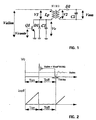
- A flyback DC-DC converter, self-oscillating in a quasi resonant manner (QRC) during steady state operation, employing a flyback transformer for storing and transferring energy to a load having an auxiliary winding (AUX) whose voltage is compared by a comparator (COMP1) with a threshold (VREF1) to detect its crossing and as a consequence switch on through a control flip-flop (FF) a power transistor (POWER) driving the primary winding of said transformer for a new phase of conduction and accumulation of energy, whose duration is established by a secondary control loop of the output voltage (ERROR AMP, CONTROL) producing the switching off of the power transistor for a successive energy transfer phase toward the load of the energy stored in the transformer during the preceding conduction phase, characterized in that the switchings control circuit is wholly integrated and comprisesa second comparator (HVCOMP) of the voltage existing on the current terminal of said power transistor (POWER) connected to the primary winding of the transformer in respect to the ground potential of the circuit;a logic gate (OR) having a first input connected to the output of said second comparator (HVCOMP) and an output coupled to the set terminal of said control flip-flop (FF);a delay network (ON DELAY) coupled in cascade to the output of said first comparator (COMP1) and having an output coupled to a second input of said logic gate (OR), ensuring, under steady state functioning conditions of the converter, the setting of said flip-flop (FF) by said second comparator (HVCOMP) rather than by said first comparator (COMP1).
- The converter as defined in claim 1, characterized in that said second comparator (HVCOMP) is realized with components integrated with high voltage fabrication process.
Priority Applications (3)
| Application Number | Priority Date | Filing Date | Title |
|---|---|---|---|
| DE69814073T DE69814073T2 (en) | 1998-09-23 | 1998-09-23 | Fully integrated turn-on control loop of a high-voltage power transistor of a quasi-resonant flyback converter |
| EP98830554A EP0989662B1 (en) | 1998-09-23 | 1998-09-23 | Completely integrated switch-on control-loop of a high voltage power transistor of a quasi resonant flyback converter |
| US09/400,775 US6078510A (en) | 1998-09-23 | 1999-09-22 | Wholly integrated switch-on control loop of a high voltage power transistor of a quasi resonant flyback converter |
Applications Claiming Priority (1)
| Application Number | Priority Date | Filing Date | Title |
|---|---|---|---|
| EP98830554A EP0989662B1 (en) | 1998-09-23 | 1998-09-23 | Completely integrated switch-on control-loop of a high voltage power transistor of a quasi resonant flyback converter |
Publications (2)
| Publication Number | Publication Date |
|---|---|
| EP0989662A1 EP0989662A1 (en) | 2000-03-29 |
| EP0989662B1 true EP0989662B1 (en) | 2003-05-02 |
Family
ID=8236798
Family Applications (1)
| Application Number | Title | Priority Date | Filing Date |
|---|---|---|---|
| EP98830554A Expired - Lifetime EP0989662B1 (en) | 1998-09-23 | 1998-09-23 | Completely integrated switch-on control-loop of a high voltage power transistor of a quasi resonant flyback converter |
Country Status (3)
| Country | Link |
|---|---|
| US (1) | US6078510A (en) |
| EP (1) | EP0989662B1 (en) |
| DE (1) | DE69814073T2 (en) |
Cited By (1)
| Publication number | Priority date | Publication date | Assignee | Title |
|---|---|---|---|---|
| DE102011089553A1 (en) * | 2011-12-22 | 2013-06-27 | Robert Bosch Gmbh | Electronic ballast for a gas discharge lamp |
Families Citing this family (57)
| Publication number | Priority date | Publication date | Assignee | Title |
|---|---|---|---|---|
| US6233165B1 (en) * | 2000-05-15 | 2001-05-15 | Asic Advantage, Inc. | Power converter having a low voltage regulator powered from a high voltage source |
| AU2003205995A1 (en) * | 2002-03-01 | 2003-09-16 | Koninklijke Philips Electronics N.V. | Flip-flop based self-oscillating power supply |
| US7280026B2 (en) | 2002-04-18 | 2007-10-09 | Coldwatt, Inc. | Extended E matrix integrated magnetics (MIM) core |
| FR2871001A1 (en) * | 2004-05-25 | 2005-12-02 | St Microelectronics Sa | TRANSFORMER WITH MODE CHANGE AND LOW-PASTE FILTER |
| US6977824B1 (en) * | 2004-08-09 | 2005-12-20 | System General Corp. | Control circuit for controlling output current at the primary side of a power converter |
| US7362593B2 (en) * | 2004-09-16 | 2008-04-22 | System General Corp. | Switching control circuit having off-time modulation to improve efficiency of primary-side controlled power supply |
| US7362592B2 (en) * | 2004-09-16 | 2008-04-22 | System General Corp. | Switching control circuit for primary-side controlled power converters |
| US7259972B2 (en) * | 2004-10-07 | 2007-08-21 | System General Corporation | Primary-side-control power converter having a switching controller using frequency hopping and voltage and current control loops |
| US7876191B2 (en) | 2005-02-23 | 2011-01-25 | Flextronics International Usa, Inc. | Power converter employing a tapped inductor and integrated magnetics and method of operating the same |
| KR100781359B1 (en) | 2005-03-23 | 2007-11-30 | 삼성전자주식회사 | Apparatus for generating high voltage by digital control and method thereof |
| US7541793B2 (en) * | 2005-06-07 | 2009-06-02 | Delta Electronics, Inc. | Parallel power supply with active droop current sharing circuit having current limiting function |
| WO2007041898A1 (en) * | 2005-10-09 | 2007-04-19 | System General Corp. | Apparatus and method thereof for measuring output current from primary side of power converter |
| JP2008005567A (en) * | 2006-06-20 | 2008-01-10 | Sanken Electric Co Ltd | Switching power supply |
| CN101154113B (en) * | 2006-09-26 | 2010-05-12 | 尼克森微电子股份有限公司 | Quasi-resonance control circuit of power supplier and its control method |
| US7675759B2 (en) * | 2006-12-01 | 2010-03-09 | Flextronics International Usa, Inc. | Power system with power converters having an adaptive controller |
| US9197132B2 (en) * | 2006-12-01 | 2015-11-24 | Flextronics International Usa, Inc. | Power converter with an adaptive controller and method of operating the same |
| KR101052426B1 (en) * | 2007-01-19 | 2011-07-27 | 신덴겐코교 가부시키가이샤 | Switching power supply |
| US7468649B2 (en) | 2007-03-14 | 2008-12-23 | Flextronics International Usa, Inc. | Isolated power converter |
| US7906941B2 (en) | 2007-06-19 | 2011-03-15 | Flextronics International Usa, Inc. | System and method for estimating input power for a power processing circuit |
| WO2009046603A1 (en) * | 2007-10-10 | 2009-04-16 | Hong Kong Applied Science And Technology Research Institute Co. Ltd. | Low voltage synchronous oscillator for dc-dc converter |
| KR101468719B1 (en) * | 2008-03-12 | 2014-12-05 | 페어차일드코리아반도체 주식회사 | Power converter and driving method thereof |
| JP5654982B2 (en) * | 2008-03-26 | 2015-01-14 | エンフェイズ エナジー インコーポレイテッド | Method and apparatus for extending the range of zero voltage switching in a DC / DC converter |
| CN102217181B (en) * | 2008-11-14 | 2014-09-03 | 伟创力国际美国公司 | Driver for a synchronous rectifier and power converter employing the same |
| US9088216B2 (en) * | 2009-01-19 | 2015-07-21 | Power Systems Technologies, Ltd. | Controller for a synchronous rectifier switch |
| CN102342007B (en) | 2009-01-19 | 2015-01-07 | 伟创力国际美国公司 | Controller for a power converter |
| US9019061B2 (en) | 2009-03-31 | 2015-04-28 | Power Systems Technologies, Ltd. | Magnetic device formed with U-shaped core pieces and power converter employing the same |
| US8643222B2 (en) | 2009-06-17 | 2014-02-04 | Power Systems Technologies Ltd | Power adapter employing a power reducer |
| US9077248B2 (en) | 2009-06-17 | 2015-07-07 | Power Systems Technologies Ltd | Start-up circuit for a power adapter |
| US8514593B2 (en) | 2009-06-17 | 2013-08-20 | Power Systems Technologies, Ltd. | Power converter employing a variable switching frequency and a magnetic device with a non-uniform gap |
| US8638578B2 (en) * | 2009-08-14 | 2014-01-28 | Power System Technologies, Ltd. | Power converter including a charge pump employable in a power adapter |
| US8976549B2 (en) | 2009-12-03 | 2015-03-10 | Power Systems Technologies, Ltd. | Startup circuit including first and second Schmitt triggers and power converter employing the same |
| US8520420B2 (en) | 2009-12-18 | 2013-08-27 | Power Systems Technologies, Ltd. | Controller for modifying dead time between switches in a power converter |
| US9246391B2 (en) | 2010-01-22 | 2016-01-26 | Power Systems Technologies Ltd. | Controller for providing a corrected signal to a sensed peak current through a circuit element of a power converter |
| US8787043B2 (en) | 2010-01-22 | 2014-07-22 | Power Systems Technologies, Ltd. | Controller for a power converter and method of operating the same |
| US8767418B2 (en) | 2010-03-17 | 2014-07-01 | Power Systems Technologies Ltd. | Control system for a power converter and method of operating the same |
| US8164928B2 (en) * | 2010-04-28 | 2012-04-24 | System General Corporation | Method and apparatus of operating a primary-side-regulation power converter at both continuous current mode and discontinuous current mode |
| US8792257B2 (en) | 2011-03-25 | 2014-07-29 | Power Systems Technologies, Ltd. | Power converter with reduced power dissipation |
| US8792256B2 (en) | 2012-01-27 | 2014-07-29 | Power Systems Technologies Ltd. | Controller for a switch and method of operating the same |
| US9190898B2 (en) | 2012-07-06 | 2015-11-17 | Power Systems Technologies, Ltd | Controller for a power converter and method of operating the same |
| US9106130B2 (en) | 2012-07-16 | 2015-08-11 | Power Systems Technologies, Inc. | Magnetic device and power converter employing the same |
| US9099232B2 (en) | 2012-07-16 | 2015-08-04 | Power Systems Technologies Ltd. | Magnetic device and power converter employing the same |
| US9379629B2 (en) | 2012-07-16 | 2016-06-28 | Power Systems Technologies, Ltd. | Magnetic device and power converter employing the same |
| US9214264B2 (en) | 2012-07-16 | 2015-12-15 | Power Systems Technologies, Ltd. | Magnetic device and power converter employing the same |
| JP5983172B2 (en) * | 2012-08-10 | 2016-08-31 | 富士電機株式会社 | Switching power supply device and switching power supply control circuit |
| ITMI20121799A1 (en) * | 2012-10-24 | 2014-04-25 | Greenventive Ltd | SEPIC CONVERTER WITH GALVANIC INSULATION |
| US9240712B2 (en) | 2012-12-13 | 2016-01-19 | Power Systems Technologies Ltd. | Controller including a common current-sense device for power switches of a power converter |
| KR101388775B1 (en) | 2012-12-20 | 2014-04-23 | 삼성전기주식회사 | Power supply device |
| KR101350575B1 (en) | 2012-12-20 | 2014-01-13 | 삼성전기주식회사 | Flyback converter |
| US9401657B2 (en) * | 2013-03-13 | 2016-07-26 | Power Integrations, Inc. | Input voltage sensor responsive to load conditions |
| CN103347334A (en) * | 2013-06-27 | 2013-10-09 | 浙江生辉照明有限公司 | Drive circuit and drive method of LED illuminating device |
| US9300206B2 (en) | 2013-11-15 | 2016-03-29 | Power Systems Technologies Ltd. | Method for estimating power of a power converter |
| CN103683867B (en) * | 2013-12-06 | 2016-03-30 | 深圳市华星光电技术有限公司 | Inverse-excitation type switch power-supply circuit and apply the backlight driving device of this circuit |
| CN103997228A (en) * | 2014-06-11 | 2014-08-20 | 航天长峰朝阳电源有限公司 | DC/DC power module with input end and output end with ultrahigh isolation voltage |
| CN105450023B (en) * | 2015-12-31 | 2018-09-14 | 杰华特微电子(杭州)有限公司 | A kind of switch controlled circuit |
| CN109995254B (en) * | 2017-12-29 | 2020-12-29 | 东南大学 | Method for improving dynamic performance of synchronous rectification primary side feedback flyback power supply |
| US10205381B1 (en) * | 2018-05-10 | 2019-02-12 | Vlt, Inc. | Start-up control in power systems using fixed-ratio power conversion |
| CN111969858A (en) * | 2020-08-25 | 2020-11-20 | 特变电工西安柔性输配电有限公司 | High-order energy-taking power circuit and control method thereof |
Family Cites Families (7)
| Publication number | Priority date | Publication date | Assignee | Title |
|---|---|---|---|---|
| US4462069A (en) * | 1981-08-14 | 1984-07-24 | American Standard Inc. | d.c. To d.c. voltage regulator having an input protection circuit, a d.c. to d.c. inverter, a saturable reactor regulator, and main and auxiliary rectifying and filtering circuits |
| CA1239986A (en) * | 1985-02-06 | 1988-08-02 | Reliance Electric Company | Control of a series resonant converter |
| DE4122544C1 (en) * | 1991-07-08 | 1992-07-16 | Braun Ag, 6000 Frankfurt, De | |
| DE59400222D1 (en) * | 1993-02-05 | 1996-05-30 | Siemens Ag | Method for limiting the frequency of a voltage-controlled oscillator in a control circuit of a resonance converter switching power supply and control circuit for a resonance converter switching power supply |
| GB2298532A (en) * | 1995-02-28 | 1996-09-04 | Ibm | Switch mode power supply |
| US5717578A (en) * | 1996-02-07 | 1998-02-10 | Emerging Technologies Corporation | Constant current source employing power conversion circuitry |
| TW344163B (en) * | 1996-09-12 | 1998-11-01 | Thomson Consumer Electronics | Self oscillating proportional drive zero voltage switching power supply |
-
1998
- 1998-09-23 DE DE69814073T patent/DE69814073T2/en not_active Expired - Lifetime
- 1998-09-23 EP EP98830554A patent/EP0989662B1/en not_active Expired - Lifetime
-
1999
- 1999-09-22 US US09/400,775 patent/US6078510A/en not_active Expired - Lifetime
Cited By (1)
| Publication number | Priority date | Publication date | Assignee | Title |
|---|---|---|---|---|
| DE102011089553A1 (en) * | 2011-12-22 | 2013-06-27 | Robert Bosch Gmbh | Electronic ballast for a gas discharge lamp |
Also Published As
| Publication number | Publication date |
|---|---|
| EP0989662A1 (en) | 2000-03-29 |
| DE69814073D1 (en) | 2003-06-05 |
| US6078510A (en) | 2000-06-20 |
| DE69814073T2 (en) | 2004-01-22 |
Similar Documents
| Publication | Publication Date | Title |
|---|---|---|
| EP0989662B1 (en) | Completely integrated switch-on control-loop of a high voltage power transistor of a quasi resonant flyback converter | |
| US10361633B2 (en) | Control method and device for switching power supplies having more than one control mode | |
| US5309344A (en) | Dual active clamp, zero voltage switching power converter | |
| US7692937B2 (en) | Resonant converter and voltage stabilizing method thereof | |
| US6118675A (en) | Method and apparatus for controlling power transfer in a flyback converter by modulating the power switch off time during transient conditions | |
| KR100378801B1 (en) | Direct current source circuit | |
| US6061252A (en) | Switching power supply device | |
| US7773392B2 (en) | Isolated switching power supply apparatus | |
| US4785387A (en) | Resonant converters with secondary-side resonance | |
| US5532577A (en) | Method and apparatus for multiple output regulation in a step-down switching regulator | |
| US6714428B2 (en) | Combined transformer-inductor device for application to DC-to-DC converter with synchronous rectifier | |
| Oruganti et al. | Soft-switched DC/DC converter with PWM control | |
| US20180248485A1 (en) | Variable blanking frequency for resonant converters | |
| KR101236955B1 (en) | Switching mode power supply and the driving method thereof | |
| KR20040068239A (en) | Flyback Power Converter | |
| Smith et al. | Controlling a DC-DC converter by using the power MOSFET as a voltage controlled resistor | |
| WO2003092328A2 (en) | Llc half-bridge converter | |
| US6078509A (en) | Multiple output flyback converter having improved cross-regulation and method of operation thereof | |
| JP2769451B2 (en) | Quantized power converter | |
| US20240113630A1 (en) | Isolated switching converter with two isolated channels and control method thereof | |
| CN111030479A (en) | Active clamp flyback power converter and related control method | |
| US5936853A (en) | Power converter having a low-loss clamp and method of operation thereof | |
| EP0949751A2 (en) | Generator for arc welding machines with forward topology and active clamp | |
| JP2604302Y2 (en) | Resonant DC-DC converter | |
| JP2605664Y2 (en) | Push-pull DC-DC converter |
Legal Events
| Date | Code | Title | Description |
|---|---|---|---|
| PUAI | Public reference made under article 153(3) epc to a published international application that has entered the european phase |
Free format text: ORIGINAL CODE: 0009012 |
|
| AK | Designated contracting states |
Kind code of ref document: A1 Designated state(s): DE FR GB IT |
|
| AX | Request for extension of the european patent |
Free format text: AL;LT;LV;MK;RO;SI |
|
| 17P | Request for examination filed |
Effective date: 20000427 |
|
| AKX | Designation fees paid |
Free format text: DE FR GB IT |
|
| 17Q | First examination report despatched |
Effective date: 20020208 |
|
| GRAH | Despatch of communication of intention to grant a patent |
Free format text: ORIGINAL CODE: EPIDOS IGRA |
|
| GRAH | Despatch of communication of intention to grant a patent |
Free format text: ORIGINAL CODE: EPIDOS IGRA |
|
| GRAA | (expected) grant |
Free format text: ORIGINAL CODE: 0009210 |
|
| AK | Designated contracting states |
Designated state(s): DE FR GB IT |
|
| REG | Reference to a national code |
Ref country code: GB Ref legal event code: FG4D |
|
| REF | Corresponds to: |
Ref document number: 69814073 Country of ref document: DE Date of ref document: 20030605 Kind code of ref document: P |
|
| ET | Fr: translation filed | ||
| PLBE | No opposition filed within time limit |
Free format text: ORIGINAL CODE: 0009261 |
|
| STAA | Information on the status of an ep patent application or granted ep patent |
Free format text: STATUS: NO OPPOSITION FILED WITHIN TIME LIMIT |
|
| 26N | No opposition filed |
Effective date: 20040203 |
|
| PGFP | Annual fee paid to national office [announced via postgrant information from national office to epo] |
Ref country code: IT Payment date: 20060930 Year of fee payment: 9 |
|
| PG25 | Lapsed in a contracting state [announced via postgrant information from national office to epo] |
Ref country code: IT Free format text: LAPSE BECAUSE OF NON-PAYMENT OF DUE FEES Effective date: 20070923 |
|
| PGFP | Annual fee paid to national office [announced via postgrant information from national office to epo] |
Ref country code: GB Payment date: 20120828 Year of fee payment: 15 |
|
| PGFP | Annual fee paid to national office [announced via postgrant information from national office to epo] |
Ref country code: FR Payment date: 20130920 Year of fee payment: 16 |
|
| GBPC | Gb: european patent ceased through non-payment of renewal fee |
Effective date: 20130923 |
|
| PG25 | Lapsed in a contracting state [announced via postgrant information from national office to epo] |
Ref country code: GB Free format text: LAPSE BECAUSE OF NON-PAYMENT OF DUE FEES Effective date: 20130923 |
|
| REG | Reference to a national code |
Ref country code: FR Ref legal event code: ST Effective date: 20150529 |
|
| PG25 | Lapsed in a contracting state [announced via postgrant information from national office to epo] |
Ref country code: FR Free format text: LAPSE BECAUSE OF NON-PAYMENT OF DUE FEES Effective date: 20140930 |
|
| PGFP | Annual fee paid to national office [announced via postgrant information from national office to epo] |
Ref country code: DE Payment date: 20170821 Year of fee payment: 20 |
|
| REG | Reference to a national code |
Ref country code: DE Ref legal event code: R071 Ref document number: 69814073 Country of ref document: DE |