EP0987818B1 - Switching amplifier for generating continuous arbitrary waveforms for magnetic resonance imaging coils - Google Patents
Switching amplifier for generating continuous arbitrary waveforms for magnetic resonance imaging coils Download PDFInfo
- Publication number
- EP0987818B1 EP0987818B1 EP99306787A EP99306787A EP0987818B1 EP 0987818 B1 EP0987818 B1 EP 0987818B1 EP 99306787 A EP99306787 A EP 99306787A EP 99306787 A EP99306787 A EP 99306787A EP 0987818 B1 EP0987818 B1 EP 0987818B1
- Authority
- EP
- European Patent Office
- Prior art keywords
- voltage
- switching
- switching amplifier
- input
- buck regulator
- Prior art date
- Legal status (The legal status is an assumption and is not a legal conclusion. Google has not performed a legal analysis and makes no representation as to the accuracy of the status listed.)
- Expired - Lifetime
Links
- 238000002595 magnetic resonance imaging Methods 0.000 title description 6
- 238000009499 grossing Methods 0.000 claims description 2
- SGPGESCZOCHFCL-UHFFFAOYSA-N Tilisolol hydrochloride Chemical compound [Cl-].C1=CC=C2C(=O)N(C)C=C(OCC(O)C[NH2+]C(C)(C)C)C2=C1 SGPGESCZOCHFCL-UHFFFAOYSA-N 0.000 claims 1
- 230000008878 coupling Effects 0.000 claims 1
- 238000010168 coupling process Methods 0.000 claims 1
- 238000005859 coupling reaction Methods 0.000 claims 1
- 238000003384 imaging method Methods 0.000 description 6
- 230000008901 benefit Effects 0.000 description 4
- 239000010752 BS 2869 Class D Substances 0.000 description 3
- 230000001276 controlling effect Effects 0.000 description 3
- 239000004065 semiconductor Substances 0.000 description 2
- 230000007704 transition Effects 0.000 description 2
- 230000008859 change Effects 0.000 description 1
- 230000000694 effects Effects 0.000 description 1
- 230000007383 nerve stimulation Effects 0.000 description 1
- 238000005457 optimization Methods 0.000 description 1
- 230000010363 phase shift Effects 0.000 description 1
- 230000009467 reduction Effects 0.000 description 1
- 230000001105 regulatory effect Effects 0.000 description 1
- 230000004044 response Effects 0.000 description 1
Images


Classifications
-
- H—ELECTRICITY
- H03—ELECTRONIC CIRCUITRY
- H03F—AMPLIFIERS
- H03F3/00—Amplifiers with only discharge tubes or only semiconductor devices as amplifying elements
- H03F3/20—Power amplifiers, e.g. Class B amplifiers, Class C amplifiers
- H03F3/21—Power amplifiers, e.g. Class B amplifiers, Class C amplifiers with semiconductor devices only
- H03F3/217—Class D power amplifiers; Switching amplifiers
- H03F3/2171—Class D power amplifiers; Switching amplifiers with field-effect devices
-
- G—PHYSICS
- G01—MEASURING; TESTING
- G01R—MEASURING ELECTRIC VARIABLES; MEASURING MAGNETIC VARIABLES
- G01R33/00—Arrangements or instruments for measuring magnetic variables
- G01R33/20—Arrangements or instruments for measuring magnetic variables involving magnetic resonance
- G01R33/28—Details of apparatus provided for in groups G01R33/44 - G01R33/64
- G01R33/38—Systems for generation, homogenisation or stabilisation of the main or gradient magnetic field
- G01R33/385—Systems for generation, homogenisation or stabilisation of the main or gradient magnetic field using gradient magnetic field coils
- G01R33/3852—Gradient amplifiers; means for controlling the application of a gradient magnetic field to the sample, e.g. a gradient signal synthesizer
Definitions
- the present invention relates generally to a switching amplifier useful for driving a gradient coil in a magnetic resonance imaging (MRI) system and, more particularly, to such an amplifier which is capable of continuous arbitrary waveform generation.
- MRI magnetic resonance imaging
- Gradient coils in MRI systems require high, rapidly changing current as well as precise current control.
- a high voltage drive is needed, requiring high-voltage, high-current semiconductors (typically insulated gate bipolar transistors , i.e., IGBT's).
- IGBT's insulated gate bipolar transistors
- Higher voltage devices generally have higher switching losses, limiting the maximum switching frequency attainable.
- With high switching losses the time interval permitted for the high-voltage inverter to switch at a sufficiently high frequency to maintain precise current waveforms is also limited.
- a solution has been to add linear amplifiers, which, unfortunately, add relatively high losses.
- the high-voltage inverter provides the high voltage needed to obtain fast current rise and fall times; and during the flat top portion of the wave which does not require high voltage, a linear amplifier controls the current
- a switching amplifier for generating arbitrary gradient coil waveforms comprises a high-frequency, reduced-voltage buck regulator, including relatively low-voltage and fast-switching devices, which controls a high-voltage bus feeding a high-voltage, full-bridge inverter.
- the reduced-voltage buck circuit When high voltage is needed, the reduced-voltage buck circuit performs the switching function to control the coil current. And when low voltage is needed, the high-voltage bridge inverter performs the switching function, but with a low-voltage dc bus applied to its input. In this manner, switching losses are shared by the buck regulator and bridge inverter and are minimized.
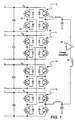
- FIG. 1 shows one conventional switching amplifier system for obtaining high voltage and a relatively high switching frequency suitable for driving a gradient coil in an MRI system.
- four full-bridge class-D switching amplifiers 10-13 each comprising four switching devices 15-18, are stacked in series with a linear amplifier 20 driving a gradient coil 22 in an MRI system.
- the dc buses feeding the amplifier may be on the order of 400 volts dc which gives a total high voltage drive of 1600 volts.
- each bridge is phase-shifted by 45 degrees with respect to the adjacent bridge, effectively multiplying the individual bridge switching frequency by a factor of eight. For example, if each bridge switches at 31.25 kHz, there is an effective coil ripple frequency of 250 kHz.
- the bridge controls the high-slew-rate current transitions, and the series-connected linear amplifier controls the current during low-slew-rate portions of the gradient current waveform.
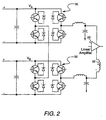
- FIG. 2 shows a system similar to that of FIG. 1 but which takes advantage of newer, higher voltage IGBT's, and thus requires only two class-D bridge amplifiers 30 and 32 in series.
- the attainable slew rate for the system of FIG. 2 is one-half that of FIG. 1, assuming the same type devices are used, but this has been found sufficient for most MRI applications since higher slew rates can lead to undesirable patient nerve stimulation.
- the lower cost system of FIG. 2 has become generally used for imaging sequences employing trapezoidal gradient current waveforms.
- the systems of FIG. 1 and FIG. 2 can generate some arbitrary current waveforms, but cannot practicably maintain such waveforms for long periods of time due to high switching losses and an attendant semiconductor device temperature rise.
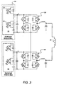
- FIG. 3 shows a system which lowers the dc bus voltage in a single step for use during the flat top portion of a trapezoidal waveform, i.e., where high voltage is not needed.
- the system of FIG. 3 includes a switched bilevel bus circuit 33 at the input of each full-bridge amplifier 30 and 32.
- Each switched bilevel bus 33 includes a half-bridge connection of switching devices 38 and 40. When low voltage is required from the amplifier, device 38 is turned off and device 40 is turned on. Bridge switching losses are reduced because these losses are approximately proportional to the dc bus voltage provided thereto.
- the amplifier of FIG. 3 is described in US Pat. No. 5,663,647 and is commonly referred to as a Gradient Amplifier Switched Bilevel Bus.
- FIG. 4 illustrates a switching amplifier 50 for generating arbitrary gradient coil waveforms in accordance with preferred embodiments of the present invention.
- two full-bridge class-D switching amplifiers 52 and 54 are connected in series.
- Switching amplifiers 52 and 54 each comprise switching devices 56-59.
- Power is supplied to the switching amplifiers via isolated dc bus voltages V A and V B , which can range, for example, up to 750 volts dc.
- the isolated dc bus voltages are each supplied by a bi-directional buck converter 46.
- Each buck converter obtains its dc bus voltage V 1 from a line-interface power supply 55 (P 1 ).
- Each power supply and buck converter combination comprises a variable bus regulator 56.
- Switching device control is represented in FIG. 4 by a block 70.
- a filter 72 at the output of the buck regulator comprises inductance 74 and capacitance 76 for smoothing current.
- the switching devices (60, 62) in the buck regulator need only be rated for the dc bus voltage V 1 (e.g., on the order of 400-500 Vdc), as opposed to the entire bus voltage V 1 +V 2 (e.g., on the order of 800 Vdc). As a result, lower voltage switching devices may be used in the buck regulator.
- the 750 Vdc bus is controlled by a buck regulator with only a 400 Vdc rating, which thus is referred to herein as a "partial-voltage" buck regulator.
- the switching losses of 600 volt IGBT's that can be used in the buck regulator are typically one-third those of 1200 volt IGBT's that are used in the full-bridge switching amplifier, for example, if the same type devices are used. Additionally, new higher-speed 600 volt IGBT's (devices 60 and 62) reduce the switching losses to one-eighth of the older higher voltage devices.
- the present invention takes advantage of the significantly lower switching losses of lower voltage switching devices in the reduced-voltage buck regulator, as explained hereinafter.
- the dc bus voltages V A and V B are varied rapidly between V 2 and V 1 +V 2 by suitably controlling the partial-voltage buck regulator by control 70.
- Most of the pulse width modulation (PWM) switching is performed using the lower voltage buck regulator devices. For example; if voltage levels between 400 and 750 volts are required by the coil, the voltage is regulated using buck regulator switching devices 60 and 62 that switch a dc bus of 400 Vdc, not 750 Vdc as would be the case if the full-bridge amplifiers were performing the switching function.
- the control 70 causes the output bridges to be switched simply to give the proper polarity voltage to the coil and therefore incur negligible switching losses.
- V A (and V B ) cannot be reduced below V 2 (e.g., 400 V)
- V 2 e.g. 400 V
- the output bridges begin switching in PWM fashion when these lower output voltages are needed.
- a rate of change of gradient coil current ( di / dt ) of 1500 A/msec can be obtained.
- a resulting gradient field slew rate (i.e., di / dt divided by coil gain) is approximately 176 Tesla/m/sec.
- a typical maximum slew rate of 120 Tesla/m/sec is sufficient such that the 750 Vdc bus provides margin to overcome gradient coil inductance and resistance variations.
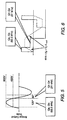
- FIG. 5 shows when the buck regulator and bridge of FIG. 4 would switch for the case of a sine wave output with slew rates requiring relatively high amplifier output voltage.
- devices 60 (Q a ) and 62 (Q b ) switch in PWM fashion when an output voltage above 400 V is needed while the output bridge simply selects the polarity to apply to the gradient coil; i.e., the output bridge is not PWM switching.
- device Q b remains on most of the time to apply V 2 to the bridge input bus V A , and the bridge devices switch in PWM fashion to regulate the output voltage.
- the lower voltage devices (60, 62) perform the switching function when high voltage is needed; and the high-voltage devices perform the switching when low output voltage is needed, but advantageously with a low applied bus voltage.
- the high-voltage devices switching with a low voltage applied bus, which advantageously results in low switching losses, but also the percentage of PWM switching time for the higher voltage devices is only about one-third, i.e., 60 out of 180° for the illustrated example.
- FIG. 6 shows the case for a trapezoidal gradient current waveform.
- devices 60 (Q a ) and 62 (Q b ) perform the switching function, and when a voltage less than V 2 is needed, the bridge performs the switching function.
- voltage V 2 can be applied directly to the coil by leaving device Qb on(e.g., during the flat top portion of a trapezoidal waveform), in which case the coil current can be controlled directly such that no device switching is needed. This results in zero amplifier switching losses.
- V 1 and V 2 are supplied from a line-interface power supply that can be controlled to be variable.
- V 1 and V 2 can be varied to achieve the best possible performance.
- An advantage of the arrangement of a switching amplifier according to the present invention is that relatively high switching frequencies can be obtained which can lead to low gradient coil ripple currents and precise current control. As a result, a linear amplifier, such as used in the circuits of FIGs. 1 and 2, is not needed.
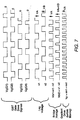
- FIG. 7 shows how the switching frequency of a bridge leg (e.g., Q 1 and Q 2 ) is multiplied by a factor of four at the gradient coil. That is, the switching frequency is multiplied by two due to the full bridge and again by two due to a 180° phase shift between the two bridges. For example, if the bridge devices are switched at 31.25 kHz, then the equivalent output switching frequency is 125 kHz. This relatively high frequency in combination with high-frequency output LC filters results in a low ripple current being applied to the gradient coil. For trapezoidal currents, such as illustrated in FIG. 6, the voltage V 2 can be controlled to this precise value (to allow the bridges to operate at a 50% duty cycle) by adjusting the input power supply.
- a bridge leg e.g., Q 1 and Q 2
- the input supply 56 (P 1 ) can be a soft-switched supply of any suitable topology, such as a phase-shifted transition resonance bridge, such as described in US Pat No. 4,864,479 or, as an alternative, a series-resonant converter. Either of these exemplary soft-switched supplies, among others, would provide a fast response, low switching loss, high efficiency supply suitable for the applications described herein. In addition, these exemplary supplies can provide a high power factor to the input ac line, if desired.
- the reduced-voltage buck regulator switching frequency is also multiplied by a factor of two if the two bridges are phase shifted 180° relative to each other, as described hereinabove. Since the devices in the buck regulator have lower switching losses than the output bridge devices, the buck regulator devices may operate at high frequencies. For example, if the buck regulators operate at 62.5 kHz, then an equivalent output switching frequency of 125 kHz results, just as in the output bridges.
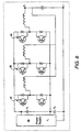
- FIG. 8 illustrates that N buck regulators can be arranged in a polyphase connection in accordance with preferred embodiments of the present invention.
- N switching regulators are operated 360 / N degrees out of phase to achieve an equivalent switching frequency of N * f .
- the switching frequency gets doubled again if the two buck regulators are phase shifted with respect to each other.
- the polyphase buck regulator which comprises lower-power regulators coupled in parallel, represents an alternative to paralleling individual devices in a single module.
- FIG. 9 illustrates an alternative embodiment of gradient amplifier, switched variable bus circuit.
- FIG. 9 differs from FIG. 4 in that the output filter 72 of each buck regulator is eliminated. Operation of the circuit of FIG. 9 is similar to that of FIG. 4 as described hereinabove with the function of filters 72 being performed by output filters 80, each comprising an inductance 82 and a capacitance 84, in combination with the gradient coil 22.
Description
- The present invention relates generally to a switching amplifier useful for driving a gradient coil in a magnetic resonance imaging (MRI) system and, more particularly, to such an amplifier which is capable of continuous arbitrary waveform generation.
- Gradient coils in MRI systems require high, rapidly changing current as well as precise current control. To achieve fast current changes, a high voltage drive is needed, requiring high-voltage, high-current semiconductors (typically insulated gate bipolar transistors , i.e., IGBT's). Higher voltage devices generally have higher switching losses, limiting the maximum switching frequency attainable. With high switching losses, the time interval permitted for the high-voltage inverter to switch at a sufficiently high frequency to maintain precise current waveforms is also limited. A solution has been to add linear amplifiers, which, unfortunately, add relatively high losses. For trapezoidal coil currents, the high-voltage inverter provides the high voltage needed to obtain fast current rise and fall times; and during the flat top portion of the wave which does not require high voltage, a linear amplifier controls the current
- Unfortunately, using linear amplifiers as described hereinabove is not practicable for arbitrary current waveforms (i.e., that are not trapezoidal) because the losses are too great to allow such waveforms to be maintained for a sufficient time to permit high-performance imaging. Hence, it is desirable to provide a switching amplifier which reduces and distributes device switching losses such that arbitrary waveforms can be maintained for extended periods of time, thereby enabling high-performance advanced imaging.
- According to the present invention, a switching amplifier for generating arbitrary gradient coil waveforms comprises a high-frequency, reduced-voltage buck regulator, including relatively low-voltage and fast-switching devices, which controls a high-voltage bus feeding a high-voltage, full-bridge inverter. When high voltage is needed, the reduced-voltage buck circuit performs the switching function to control the coil current. And when low voltage is needed, the high-voltage bridge inverter performs the switching function, but with a low-voltage dc bus applied to its input. In this manner, switching losses are shared by the buck regulator and bridge inverter and are minimized. As a result, high-frequency operation is achieved such that arbitrary coil waveforms can be generated, allowing for advanced imaging techniques such as those employing spiral trajectories. Additionally, further optimization and ripple current reduction in the gradient coil are achieved by controlling a variable input power supply to adjust the input bus voltages.
- Embodiments of the invention will now be described, by way of example, with reference to the accompanying drawings, in which:
- FIG. 1 schematically illustrates four stacked full-bridge amplifiers for obtaining high voltage and a relatively high switching frequency;
- FIG. 2 schematically illustrates a system similar to that of FIG. 1 but which utilizes higher voltage IGBT's;
- FIG. 3 schematically illustrates a gradient amplifier switched bilevel bus circuit;
- FIG. 4 schematically illustrates a gradient amplifier, switched variable bus circuit in accordance with preferred embodiments of the present invention;
- FIG. 5 graphically illustrates switching times for the buck regulator and bridge inverter of FIG. 4 for the case of a sine wave output with slew rates requiring relatively high amplifier output voltage;
- FIG. 6 graphically illustrates switching times for the buck regulator and bridge inverter for the case of a trapezoidal gradient current waveform;
- FIG. 7 graphically illustrates how the switching frequency of an inverter bridge leg is multiplied by a factor of four at the gradient coil in accordance with preferred embodiments of the present invention;
- FIG. 8 schematically illustrates a polyphase partial-voltage buck regulator; and
- FIG. 9 schematically illustrates an alternative embodiment of a gradient amplifier, switched variable bus circuit of the present invention.
-
- FIG. 1 shows one conventional switching amplifier system for obtaining high voltage and a relatively high switching frequency suitable for driving a gradient coil in an MRI system. As shown, four full-bridge class-D switching amplifiers 10-13, each comprising four switching devices 15-18, are stacked in series with a
linear amplifier 20 driving agradient coil 22 in an MRI system. In a typical case, the dc buses feeding the amplifier may be on the order of 400 volts dc which gives a total high voltage drive of 1600 volts. In switching, each bridge is phase-shifted by 45 degrees with respect to the adjacent bridge, effectively multiplying the individual bridge switching frequency by a factor of eight. For example, if each bridge switches at 31.25 kHz, there is an effective coil ripple frequency of 250 kHz. The bridge controls the high-slew-rate current transitions, and the series-connected linear amplifier controls the current during low-slew-rate portions of the gradient current waveform. - FIG. 2 shows a system similar to that of FIG. 1 but which takes advantage of newer, higher voltage IGBT's, and thus requires only two class-
D bridge amplifiers - FIG. 3 shows a system which lowers the dc bus voltage in a single step for use during the flat top portion of a trapezoidal waveform, i.e., where high voltage is not needed. The system of FIG. 3 includes a switched
bilevel bus circuit 33 at the input of each full-bridge amplifier bilevel bus 33 includes a half-bridge connection ofswitching devices device 38 is turned off anddevice 40 is turned on. Bridge switching losses are reduced because these losses are approximately proportional to the dc bus voltage provided thereto. The amplifier of FIG. 3 is described in US Pat. No. 5,663,647 and is commonly referred to as a Gradient Amplifier Switched Bilevel Bus. With such a system, the linear amplifier which adds high losses may be eliminated, and precise current control may be maintained during the flat top portions of trapezoidal current waveforms. However, this system is optimized only for trapezoidal waveforms. For arbitrary waveforms, such as sine waves used in more advanced spiral imaging techniques, the high-voltage bus must remain connected for most of the waveform, resulting in high switching losses. Hence, an arbitrary waveform cannot be maintained for long due to excessive IGBT switching losses. - FIG. 4 illustrates a
switching amplifier 50 for generating arbitrary gradient coil waveforms in accordance with preferred embodiments of the present invention. In the embodiment of FIG. 4, two full-bridge class-D switching amplifiers amplifiers bi-directional buck converter 46. Each buck converter obtains its dc bus voltage V1 from a line-interface power supply 55 (P1). Each power supply and buck converter combination comprises avariable bus regulator 56. Switching device control is represented in FIG. 4 by ablock 70. Afilter 72 at the output of the buck regulator comprisesinductance 74 andcapacitance 76 for smoothing current. - The switching devices (60, 62) in the buck regulator need only be rated for the dc bus voltage V1 (e.g., on the order of 400-500 Vdc), as opposed to the entire bus voltage V1+V2 (e.g., on the order of 800 Vdc). As a result, lower voltage switching devices may be used in the buck regulator. In effect, the 750 Vdc bus is controlled by a buck regulator with only a 400 Vdc rating, which thus is referred to herein as a "partial-voltage" buck regulator. The switching losses of 600 volt IGBT's that can be used in the buck regulator, for example, are typically one-third those of 1200 volt IGBT's that are used in the full-bridge switching amplifier, for example, if the same type devices are used. Additionally, new higher-speed 600 volt IGBT's (
devices 60 and 62) reduce the switching losses to one-eighth of the older higher voltage devices. The present invention takes advantage of the significantly lower switching losses of lower voltage switching devices in the reduced-voltage buck regulator, as explained hereinafter. - In accordance with preferred embodiments of the present invention, the dc bus voltages VA and VB are varied rapidly between V2 and V1+V2 by suitably controlling the partial-voltage buck regulator by
control 70. Most of the pulse width modulation (PWM) switching is performed using the lower voltage buck regulator devices. For example; if voltage levels between 400 and 750 volts are required by the coil, the voltage is regulated using buckregulator switching devices control 70 causes the output bridges to be switched simply to give the proper polarity voltage to the coil and therefore incur negligible switching losses. Since the voltage VA (and VB) cannot be reduced below V2 (e.g., 400 V), the output bridges begin switching in PWM fashion when these lower output voltages are needed. During this time, the input buck regulator is not switching, and is thus not producing any switching losses, but the output bridges are switching with a reduced dc bus voltage (e.g., V2=400 Vdc). Since switching losses are approximately proportional to the dc bus voltage, the switching losses of the output bridge at the reduced bus voltage are significantly lower. By controlling the overall amplifier in this manner, switching losses are reduced and distributed over several devices. - For example, in the embodiment of FIG. 4 with a typical gradient coil inductance around 1 mH, a rate of change of gradient coil current (di/dt) of 1500 A/msec can be obtained. For a typical coil gain of 85 A/Gauss/cm, a resulting gradient field slew rate (i.e., di/dt divided by coil gain) is approximately 176 Tesla/m/sec. A typical maximum slew rate of 120 Tesla/m/sec is sufficient such that the 750 Vdc bus provides margin to overcome gradient coil inductance and resistance variations.
- FIG. 5 shows when the buck regulator and bridge of FIG. 4 would switch for the case of a sine wave output with slew rates requiring relatively high amplifier output voltage. Assuming that V1=V2=400 Vdc, devices 60 (Qa) and 62 (Qb) switch in PWM fashion when an output voltage above 400 V is needed while the output bridge simply selects the polarity to apply to the gradient coil; i.e., the output bridge is not PWM switching. When an output voltage below 400 V is needed, device Qb remains on most of the time to apply V2 to the bridge input bus VA, and the bridge devices switch in PWM fashion to regulate the output voltage. The lower voltage devices (60, 62) perform the switching function when high voltage is needed; and the high-voltage devices perform the switching when low output voltage is needed, but advantageously with a low applied bus voltage. Not only are the high-voltage devices switching with a low voltage applied bus, which advantageously results in low switching losses, but also the percentage of PWM switching time for the higher voltage devices is only about one-third, i.e., 60 out of 180° for the illustrated example.
- FIG. 6 shows the case for a trapezoidal gradient current waveform. When a voltage greater than V2 is needed, devices 60 (Qa) and 62 (Qb)perform the switching function, and when a voltage less than V2 is needed, the bridge performs the switching function.
- Further, voltage V2 can be applied directly to the coil by leaving device Qb on(e.g., during the flat top portion of a trapezoidal waveform), in which case the coil current can be controlled directly such that no device switching is needed. This results in zero amplifier switching losses.
- The voltages V1 and V2 are supplied from a line-interface power supply that can be controlled to be variable. Thus, for a given imaging sequence, V1 and V2, either in proportion or separately, can be varied to achieve the best possible performance.
- An advantage of the arrangement of a switching amplifier according to the present invention is that relatively high switching frequencies can be obtained which can lead to low gradient coil ripple currents and precise current control. As a result, a linear amplifier, such as used in the circuits of FIGs. 1 and 2, is not needed.
- FIG. 7 shows how the switching frequency of a bridge leg (e.g., Q1 and Q2) is multiplied by a factor of four at the gradient coil. That is, the switching frequency is multiplied by two due to the full bridge and again by two due to a 180° phase shift between the two bridges. For example, if the bridge devices are switched at 31.25 kHz, then the equivalent output switching frequency is 125 kHz. This relatively high frequency in combination with high-frequency output LC filters results in a low ripple current being applied to the gradient coil. For trapezoidal currents, such as illustrated in FIG. 6, the voltage V2 can be controlled to this precise value (to allow the bridges to operate at a 50% duty cycle) by adjusting the input power supply. In this case, very low output ripple results, theoretically zero. Output current ripple can also be effectively eliminated during flat top portion of the trapezoidal current waveform if the input power supply regulates voltage V2 voltage to the value necessary to overcome conduction losses in the power converters and the gradient coil. This approach provides an added benefit of essentially eliminating switching losses in both buck regulators and output bridges since they are all continuously conducting during the flat top portion of the waveform.
- The input supply 56 (P1) can be a soft-switched supply of any suitable topology, such as a phase-shifted transition resonance bridge, such as described in US Pat No. 4,864,479 or, as an alternative, a series-resonant converter. Either of these exemplary soft-switched supplies, among others, would provide a fast response, low switching loss, high efficiency supply suitable for the applications described herein. In addition, these exemplary supplies can provide a high power factor to the input ac line, if desired.
- The reduced-voltage buck regulator switching frequency is also multiplied by a factor of two if the two bridges are phase shifted 180° relative to each other, as described hereinabove. Since the devices in the buck regulator have lower switching losses than the output bridge devices, the buck regulator devices may operate at high frequencies. For example, if the buck regulators operate at 62.5 kHz, then an equivalent output switching frequency of 125 kHz results, just as in the output bridges.
- FIG. 8 illustrates that N buck regulators can be arranged in a polyphase connection in accordance with preferred embodiments of the present invention. Here, N switching regulators are operated 360/N degrees out of phase to achieve an equivalent switching frequency of N*f. And the switching frequency gets doubled again if the two buck regulators are phase shifted with respect to each other. The polyphase buck regulator, which comprises lower-power regulators coupled in parallel, represents an alternative to paralleling individual devices in a single module.
- FIG. 9 illustrates an alternative embodiment of gradient amplifier, switched variable bus circuit. In particular, FIG. 9 differs from FIG. 4 in that the
output filter 72 of each buck regulator is eliminated. Operation of the circuit of FIG. 9 is similar to that of FIG. 4 as described hereinabove with the function offilters 72 being performed byoutput filters 80, each comprising aninductance 82 and acapacitance 84, in combination with thegradient coil 22.
Claims (13)
- A switching amplifier having two paths, each path comprising:an isolated dc output voltage bus (VA,VB);first (V1, V3) and second (V2, V4) input voltage buses;an input buck regulator (46) for controlling said isolated dc output voltage bus, the input buck regulator coupled across the first input voltage bus which is in series with the second input voltage bus, the first and second input voltage buses being adapted for coupling to an input power supply (55), the voltage on said isolated dc output voltage bus being greater than the voltage on the second input voltage bus during normal running operation;a bridge inverter (52,54) coupled to said isolated dc output voltage bus for providing a voltage to a load (22);the switching amplifier further comprising:a switching control (70) for controlling the input buck regulator to regulate for load voltages above a threshold voltage only, and for controlling the bridge inverters to regulate for load voltages below the threshold only.
- The switching amplifier of claim 1 wherein the isolated voltage buses comprise variable voltage buses.
- The switching amplifier of claim 1 wherein the switching control controls the input buck regulator and the bridge inverters to switch in a PWM mode.
- The switching amplifier of claim 1 wherein the buck regulators are coupled to receive power from a variable input power supply.
- The switching amplifier of claim 4 wherein the variable input power supply comprises a high power factor supply.
- The switching amplifier of claim 1 wherein the bridge inverters are phase-shifted with respect to each other.
- The switching amplifier of claim 1 wherein the input buck regulators comprise polyphase buck regulators.
- The switching amplifier of claim 1 wherein the input buck regulator comprises a partial-voltage buck regulator with a voltage rating equal to a portion of the voltage rating of the bridge inverters.
- The switching amplifier of claim 1 wherein the bridge inverters have a duty cycle of approximately 50%.
- The switching amplifier of claim 1 wherein the switching control controls the second voltage bus without switching devices in the buck regulator or bridge inverters in order to apply the voltage on the second voltage bus directly to the load.
- The switching amplifier of claim 1, further comprising filter means for smoothing current provided to the load.
- The switching amplifier of claim 11 wherein the filter means comprises an output filter (72) coupled to each buck regulator.
- The switching amplifier of daim 11 wherein the filter means comprises an output filter (80) coupled to each- bridge inverter.
Applications Claiming Priority (2)
| Application Number | Priority Date | Filing Date | Title |
|---|---|---|---|
| US09/148,559 US6031746A (en) | 1998-09-04 | 1998-09-04 | Switching amplifier for generating continuous arbitrary waveforms for magnetic resonance imaging coils |
| US148559 | 1998-09-04 |
Publications (3)
| Publication Number | Publication Date |
|---|---|
| EP0987818A2 EP0987818A2 (en) | 2000-03-22 |
| EP0987818A3 EP0987818A3 (en) | 2002-03-20 |
| EP0987818B1 true EP0987818B1 (en) | 2003-12-10 |
Family
ID=22526290
Family Applications (1)
| Application Number | Title | Priority Date | Filing Date |
|---|---|---|---|
| EP99306787A Expired - Lifetime EP0987818B1 (en) | 1998-09-04 | 1999-08-26 | Switching amplifier for generating continuous arbitrary waveforms for magnetic resonance imaging coils |
Country Status (6)
| Country | Link |
|---|---|
| US (1) | US6031746A (en) |
| EP (1) | EP0987818B1 (en) |
| JP (1) | JP4362176B2 (en) |
| KR (1) | KR20000022900A (en) |
| CN (1) | CN1247319A (en) |
| DE (1) | DE69913454T2 (en) |
Families Citing this family (44)
| Publication number | Priority date | Publication date | Assignee | Title |
|---|---|---|---|---|
| US6166602A (en) * | 1999-09-27 | 2000-12-26 | General Electric Company | High-efficiency switching power amplifier |
| US6552918B1 (en) * | 2000-12-26 | 2003-04-22 | Juniper Networks, Inc. | Space-efficient power supply systems and methods with minimal heat generation |
| DE10125233C1 (en) * | 2001-05-22 | 2002-12-12 | Siemens Ag | Receiver device for magnetic resonance imaging has two receiving coils and an amplifier downstream from these coils |
| US7302011B1 (en) * | 2002-10-16 | 2007-11-27 | Rf Micro Devices, Inc. | Quadrature frequency doubling system |
| CN1735814B (en) * | 2003-01-07 | 2010-06-16 | 皇家飞利浦电子股份有限公司 | High-frequency system for an MR apparatus with multiple transmit channels and the MR apparatus therein |
| US6930483B2 (en) * | 2003-08-01 | 2005-08-16 | General Electric Company | Method/system for switched frequency ripple reduction in MRI gradient coils |
| US7116166B2 (en) * | 2004-06-15 | 2006-10-03 | General Electric Company | High fidelity, high power switched amplifier |
| EP2464000A3 (en) * | 2005-02-25 | 2017-08-30 | Mitsubishi Denki Kabushiki Kaisha | Power conversion apparatus |
| EP1852964B1 (en) * | 2005-02-25 | 2012-01-18 | Mitsubishi Denki Kabushiki Kaisha | Power conversion apparatus |
| US7336059B2 (en) * | 2005-11-15 | 2008-02-26 | General Electric Company | System and method for charging and discharging a superconducting coil |
| KR101122390B1 (en) * | 2007-02-01 | 2012-03-23 | 제이엠 일렉트로닉스 엘티디. 엘엘씨 | Method and system for increasing sampling frequency for switching amplifiers |
| US7508096B1 (en) * | 2007-09-20 | 2009-03-24 | General Electric Company | Switching circuit apparatus having a series conduction path for servicing a load and switching method |
| EP2234237A1 (en) * | 2009-03-26 | 2010-09-29 | ABB Research Ltd. | Method for controlling single-phase DC/AC converters and converter arrangement |
| EP2234263A1 (en) * | 2009-03-27 | 2010-09-29 | Koninklijke Philips Electronics N.V. | A power supply, method, and computer program product for supplying electrical power to a load |
| WO2010114088A1 (en) * | 2009-04-03 | 2010-10-07 | 株式会社小松製作所 | Control device for transformer coupling type booster |
| CN102263542B (en) | 2010-05-31 | 2015-11-25 | Ge医疗系统环球技术有限公司 | Phase shifter and power amplifier thereof and magnetic resonance imaging device |
| JP5780512B2 (en) * | 2010-06-07 | 2015-09-16 | 株式会社東芝 | Magnetic resonance imaging system |
| CN102947720B (en) * | 2010-06-17 | 2015-07-08 | 皇家飞利浦电子股份有限公司 | Gradient coil power supply and a magnetic resonance imaging system |
| JP5731328B2 (en) * | 2011-08-30 | 2015-06-10 | ジーイー・メディカル・システムズ・グローバル・テクノロジー・カンパニー・エルエルシー | Inverter device and MR device |
| MX2014003549A (en) | 2011-09-27 | 2014-05-28 | Koninkl Philips Nv | Gradient amplifier with compensation for dead time and forward voltage. |
| CN102508183B (en) * | 2011-11-11 | 2013-09-11 | 辽宁开普医疗系统有限公司 | Digital variable frequency PWM (Pulse Width Modulation) gradient amplifier with adaptively-controlled load |
| CN103176150B (en) | 2011-12-21 | 2015-08-26 | 通用电气公司 | Gradient amplifier system and control method thereof |
| RU2014141084A (en) * | 2012-03-12 | 2016-05-10 | Конинклейке Филипс Н.В. | POWER TRANSMITTER FOR POWER SUPPLY OF A GRADIENT COIL FOR MAGNETIC RESONANT TOMOGRAPHY (MRI) AND METHOD OF FUNCTIONING A POWER TRANSDUCER |
| CN104583793B (en) * | 2012-07-25 | 2019-07-16 | 皇家飞利浦有限公司 | The MRI gradient amplifier that can be worked in different switching rate |
| US9344042B2 (en) * | 2013-02-27 | 2016-05-17 | Hengchun Mao | High efficiency power amplifiers with advanced power solutions |
| US10270439B2 (en) * | 2013-02-27 | 2019-04-23 | Hengchun Mao | High efficiency resonant power converters and resonant gate drivers |
| CN104142483B (en) * | 2013-05-07 | 2017-07-07 | 辽宁开普医疗系统有限公司 | A kind of small ripple gradient amplifier of high-voltage great-current |
| CN103414362B (en) * | 2013-08-23 | 2015-12-09 | 东南大学 | A kind of programmable voltage waveform generation equipment based on general voltage control strategy |
| CN104518664B (en) * | 2013-09-29 | 2017-10-03 | 西门子(深圳)磁共振有限公司 | A kind of magnetic resonance imaging system and its coil control device |
| EP2910965A1 (en) * | 2014-02-19 | 2015-08-26 | Albert-Ludwigs-Universität Freiburg | Multi-channel switching system for MRI matrix gradient coils |
| CN105471393B (en) * | 2014-09-12 | 2018-12-18 | 通用电气公司 | The switching amplifier operated with zero voltage switch and thermal equilibrium control algorithm |
| CN105703631B (en) * | 2014-11-25 | 2018-12-25 | 上海联影医疗科技有限公司 | Gradient amplifier power cell, gradient amplifier and magnetic resonance imaging system |
| CN105703726B (en) * | 2014-11-28 | 2021-04-20 | Ge医疗系统环球技术有限公司 | Power amplifier, power supply device and magnetic resonance imaging equipment |
| DE102014118040B4 (en) * | 2014-12-05 | 2017-08-24 | Fraunhofer-Gesellschaft zur Förderung der angewandten Forschung e.V. | Control circuit for a base station for transmitting energy to a receiver by means of an electrical resonant circuit, evaluation device, method and computer program |
| WO2016168249A1 (en) | 2015-04-13 | 2016-10-20 | Hyperfine Research, Inc. | Magnetic coil power methods and apparatus |
| US9807863B1 (en) * | 2016-06-09 | 2017-10-31 | Advanced Energy Industries, Inc. | Switching amplifier |
| USD876628S1 (en) | 2016-07-20 | 2020-02-25 | Nyxoah S.A. | Medical implant |
| USD988519S1 (en) | 2016-09-12 | 2023-06-06 | Nyxoah S.A. | Patch |
| EP3589358A1 (en) | 2017-02-28 | 2020-01-08 | Nyxoah SA | Surgical implant system |
| CN108173417B (en) | 2018-01-11 | 2020-06-16 | 台达电子企业管理(上海)有限公司 | Gradient power supply driving stage circuit, gradient power supply system and control method thereof |
| US11968771B2 (en) | 2018-11-09 | 2024-04-23 | Prodrive Technologies Innovation Services B.V. | Voltage waveform generator for plasma processing apparatuses |
| NL2022222B1 (en) * | 2018-12-17 | 2020-07-03 | Prodrive Tech Bv | Voltage waveform generator for plasma processing apparatuses |
| NL2022999B1 (en) | 2019-04-24 | 2020-11-02 | Prodrive Tech Bv | Voltage waveform generator for plasma processing apparatuses |
| WO2024089751A1 (en) * | 2022-10-25 | 2024-05-02 | 三菱電機株式会社 | High voltage pulse power supply device, gas laser oscillator, and laser processing machine |
Family Cites Families (7)
| Publication number | Priority date | Publication date | Assignee | Title |
|---|---|---|---|---|
| US4468626A (en) * | 1982-01-25 | 1984-08-28 | Harris Corporation | Polyphase PDM amplifier |
| EP0250718A1 (en) * | 1986-06-30 | 1988-01-07 | Siemens Aktiengesellschaft | Current supply for an inductive load, especially a gradient coil with a control and regulation device |
| US4864479A (en) * | 1988-03-07 | 1989-09-05 | General Electric Company | Full-bridge lossless switching converter |
| EP0732004B1 (en) * | 1993-11-30 | 1998-04-29 | Crown International Inc. | Switch-mode power supply for a power amplifier |
| US5576940A (en) * | 1995-01-09 | 1996-11-19 | General Electric Company | Front-end power converter for distributed power systems |
| US5663647A (en) * | 1995-12-29 | 1997-09-02 | General Electric Company | Switching gradient amplifier with adjustable DC bus voltage |
| US5781421A (en) * | 1996-12-16 | 1998-07-14 | General Electric Company | High-frequency, high-efficiency converter with recirculating energy control for high-density power conversion |
-
1998
- 1998-09-04 US US09/148,559 patent/US6031746A/en not_active Expired - Lifetime
-
1999
- 1999-08-26 DE DE69913454T patent/DE69913454T2/en not_active Expired - Lifetime
- 1999-08-26 EP EP99306787A patent/EP0987818B1/en not_active Expired - Lifetime
- 1999-09-01 JP JP24683699A patent/JP4362176B2/en not_active Expired - Fee Related
- 1999-09-03 CN CN99118609A patent/CN1247319A/en active Pending
- 1999-09-03 KR KR1019990037300A patent/KR20000022900A/en not_active Application Discontinuation
Also Published As
| Publication number | Publication date |
|---|---|
| US6031746A (en) | 2000-02-29 |
| JP4362176B2 (en) | 2009-11-11 |
| KR20000022900A (en) | 2000-04-25 |
| DE69913454D1 (en) | 2004-01-22 |
| JP2000092856A (en) | 2000-03-31 |
| DE69913454T2 (en) | 2004-10-07 |
| CN1247319A (en) | 2000-03-15 |
| EP0987818A3 (en) | 2002-03-20 |
| EP0987818A2 (en) | 2000-03-22 |
Similar Documents
| Publication | Publication Date | Title |
|---|---|---|
| EP0987818B1 (en) | Switching amplifier for generating continuous arbitrary waveforms for magnetic resonance imaging coils | |
| US7692938B2 (en) | Multiphase power converters and multiphase power converting methods | |
| US7423894B2 (en) | Interleaved soft switching bridge power converter | |
| US5140510A (en) | Constant frequency power converter | |
| US5528480A (en) | Highly efficient rectifying and converting circuit for computer power supplies | |
| US7692936B2 (en) | Medium frequency power generator | |
| US20050242793A1 (en) | Pulse forming converter | |
| JPS63277425A (en) | Switching power-supply device | |
| KR930000416B1 (en) | Device for controlling arangement which is adapted for feeding an inductive load | |
| US6166602A (en) | High-efficiency switching power amplifier | |
| US5563775A (en) | Full bridge phase displaced resonant transition circuit for obtaining constant resonant transition current from 0° phase angle to 180° phase angle | |
| JP2005065497A (en) | Pulse-width modulation soft switching control | |
| US20170264248A1 (en) | Switching amplifier with zero voltage switching and balanced thermal control algorithm | |
| US6411534B1 (en) | Control methods for power converter circuit | |
| Fujii et al. | Class-E rectifier using thinned-out method | |
| RU2216094C2 (en) | Resonance-tuned power converter for coil excitation | |
| Steigerwald et al. | High-power, high-performance switching amplifier for driving magnetic resonance imaging gradient coils | |
| US20050212496A1 (en) | Voltage regulator | |
| JPH11155832A (en) | Power amplifier and nuclear spin tomograph | |
| US7361870B2 (en) | Supply generator for an oscillating circuit, particularly for an induction cooking hob | |
| US20230412086A1 (en) | Isolated full-bridge converter | |
| WO2019210167A1 (en) | Method for balancing loss energy distribution in a circuit driving a resonant load | |
| JPH07135769A (en) | Dc resonance converter | |
| Shahrbabaki et al. | A new gradient driver with only a single DC voltage source for using in MRI systems | |
| JP2021197758A (en) | Switching power supply device, and control device and control method thereof |
Legal Events
| Date | Code | Title | Description |
|---|---|---|---|
| PUAI | Public reference made under article 153(3) epc to a published international application that has entered the european phase |
Free format text: ORIGINAL CODE: 0009012 |
|
| AK | Designated contracting states |
Kind code of ref document: A2 Designated state(s): AT BE CH CY DE DK ES FI FR GB GR IE IT LI LU MC NL PT SE Kind code of ref document: A2 Designated state(s): DE NL |
|
| AX | Request for extension of the european patent |
Free format text: AL;LT;LV;MK;RO;SI |
|
| PUAL | Search report despatched |
Free format text: ORIGINAL CODE: 0009013 |
|
| AK | Designated contracting states |
Kind code of ref document: A3 Designated state(s): AT BE CH CY DE DK ES FI FR GB GR IE IT LI LU MC NL PT SE |
|
| AX | Request for extension of the european patent |
Free format text: AL;LT;LV;MK;RO;SI |
|
| 17P | Request for examination filed |
Effective date: 20020920 |
|
| AKX | Designation fees paid |
Free format text: DE NL |
|
| GRAH | Despatch of communication of intention to grant a patent |
Free format text: ORIGINAL CODE: EPIDOS IGRA |
|
| GRAA | (expected) grant |
Free format text: ORIGINAL CODE: 0009210 |
|
| GRAS | Grant fee paid |
Free format text: ORIGINAL CODE: EPIDOSNIGR3 |
|
| AK | Designated contracting states |
Kind code of ref document: B1 Designated state(s): DE NL |
|
| REG | Reference to a national code |
Ref country code: IE Ref legal event code: FG4D |
|
| REF | Corresponds to: |
Ref document number: 69913454 Country of ref document: DE Date of ref document: 20040122 Kind code of ref document: P |
|
| PLBE | No opposition filed within time limit |
Free format text: ORIGINAL CODE: 0009261 |
|
| STAA | Information on the status of an ep patent application or granted ep patent |
Free format text: STATUS: NO OPPOSITION FILED WITHIN TIME LIMIT |
|
| 26N | No opposition filed |
Effective date: 20040913 |
|
| REG | Reference to a national code |
Ref country code: IE Ref legal event code: MM4A |
|
| PGFP | Annual fee paid to national office [announced via postgrant information from national office to epo] |
Ref country code: NL Payment date: 20160826 Year of fee payment: 18 |
|
| PGFP | Annual fee paid to national office [announced via postgrant information from national office to epo] |
Ref country code: DE Payment date: 20160826 Year of fee payment: 18 |
|
| REG | Reference to a national code |
Ref country code: DE Ref legal event code: R119 Ref document number: 69913454 Country of ref document: DE |
|
| REG | Reference to a national code |
Ref country code: NL Ref legal event code: MM Effective date: 20170901 |
|
| PG25 | Lapsed in a contracting state [announced via postgrant information from national office to epo] |
Ref country code: NL Free format text: LAPSE BECAUSE OF NON-PAYMENT OF DUE FEES Effective date: 20170901 |
|
| PG25 | Lapsed in a contracting state [announced via postgrant information from national office to epo] |
Ref country code: DE Free format text: LAPSE BECAUSE OF NON-PAYMENT OF DUE FEES Effective date: 20180301 |