EP0884746A2 - Synchronous switching regulator which employs switch voltage-drop for current sensing - Google Patents
Synchronous switching regulator which employs switch voltage-drop for current sensing Download PDFInfo
- Publication number
- EP0884746A2 EP0884746A2 EP98110504A EP98110504A EP0884746A2 EP 0884746 A2 EP0884746 A2 EP 0884746A2 EP 98110504 A EP98110504 A EP 98110504A EP 98110504 A EP98110504 A EP 98110504A EP 0884746 A2 EP0884746 A2 EP 0884746A2
- Authority
- EP
- European Patent Office
- Prior art keywords
- circuitry
- regulator
- current
- voltage
- switching element
- Prior art date
- Legal status (The legal status is an assumption and is not a legal conclusion. Google has not performed a legal analysis and makes no representation as to the accuracy of the status listed.)
- Granted
Links
Images


Classifications
-
- H—ELECTRICITY
- H02—GENERATION; CONVERSION OR DISTRIBUTION OF ELECTRIC POWER
- H02M—APPARATUS FOR CONVERSION BETWEEN AC AND AC, BETWEEN AC AND DC, OR BETWEEN DC AND DC, AND FOR USE WITH MAINS OR SIMILAR POWER SUPPLY SYSTEMS; CONVERSION OF DC OR AC INPUT POWER INTO SURGE OUTPUT POWER; CONTROL OR REGULATION THEREOF
- H02M3/00—Conversion of dc power input into dc power output
- H02M3/02—Conversion of dc power input into dc power output without intermediate conversion into ac
- H02M3/04—Conversion of dc power input into dc power output without intermediate conversion into ac by static converters
- H02M3/10—Conversion of dc power input into dc power output without intermediate conversion into ac by static converters using discharge tubes with control electrode or semiconductor devices with control electrode
- H02M3/145—Conversion of dc power input into dc power output without intermediate conversion into ac by static converters using discharge tubes with control electrode or semiconductor devices with control electrode using devices of a triode or transistor type requiring continuous application of a control signal
- H02M3/155—Conversion of dc power input into dc power output without intermediate conversion into ac by static converters using discharge tubes with control electrode or semiconductor devices with control electrode using devices of a triode or transistor type requiring continuous application of a control signal using semiconductor devices only
- H02M3/156—Conversion of dc power input into dc power output without intermediate conversion into ac by static converters using discharge tubes with control electrode or semiconductor devices with control electrode using devices of a triode or transistor type requiring continuous application of a control signal using semiconductor devices only with automatic control of output voltage or current, e.g. switching regulators
- H02M3/158—Conversion of dc power input into dc power output without intermediate conversion into ac by static converters using discharge tubes with control electrode or semiconductor devices with control electrode using devices of a triode or transistor type requiring continuous application of a control signal using semiconductor devices only with automatic control of output voltage or current, e.g. switching regulators including plural semiconductor devices as final control devices for a single load
- H02M3/1588—Conversion of dc power input into dc power output without intermediate conversion into ac by static converters using discharge tubes with control electrode or semiconductor devices with control electrode using devices of a triode or transistor type requiring continuous application of a control signal using semiconductor devices only with automatic control of output voltage or current, e.g. switching regulators including plural semiconductor devices as final control devices for a single load comprising at least one synchronous rectifier element
-
- H—ELECTRICITY
- H02—GENERATION; CONVERSION OR DISTRIBUTION OF ELECTRIC POWER
- H02M—APPARATUS FOR CONVERSION BETWEEN AC AND AC, BETWEEN AC AND DC, OR BETWEEN DC AND DC, AND FOR USE WITH MAINS OR SIMILAR POWER SUPPLY SYSTEMS; CONVERSION OF DC OR AC INPUT POWER INTO SURGE OUTPUT POWER; CONTROL OR REGULATION THEREOF
- H02M1/00—Details of apparatus for conversion
- H02M1/0003—Details of control, feedback or regulation circuits
- H02M1/0009—Devices or circuits for detecting current in a converter
-
- Y—GENERAL TAGGING OF NEW TECHNOLOGICAL DEVELOPMENTS; GENERAL TAGGING OF CROSS-SECTIONAL TECHNOLOGIES SPANNING OVER SEVERAL SECTIONS OF THE IPC; TECHNICAL SUBJECTS COVERED BY FORMER USPC CROSS-REFERENCE ART COLLECTIONS [XRACs] AND DIGESTS
- Y02—TECHNOLOGIES OR APPLICATIONS FOR MITIGATION OR ADAPTATION AGAINST CLIMATE CHANGE
- Y02B—CLIMATE CHANGE MITIGATION TECHNOLOGIES RELATED TO BUILDINGS, e.g. HOUSING, HOUSE APPLIANCES OR RELATED END-USER APPLICATIONS
- Y02B70/00—Technologies for an efficient end-user side electric power management and consumption
- Y02B70/10—Technologies improving the efficiency by using switched-mode power supplies [SMPS], i.e. efficient power electronics conversion e.g. power factor correction or reduction of losses in power supplies or efficient standby modes
Definitions
- This invention relates to switching regulator circuits. More particularly, this invention relates to current sensing in synchronous switching regulator circuits.
- Switching regulator circuits provide loads with a predetermined and substantially constant output voltage from a source voltage which may be poorly-specified or fluctuating. Such regulators usually employ a switch, which includes one or more switching elements coupled in series or in parallel with the load; switching elements may be, for example, power MOSFETs. Control circuitry regulates the amount of current supplied to a load by varying the ON-OFF times of the switching elements (i.e., the duty cycle of the regulator, which is the percentage of time that a switch is ON during a cycle of operation). Inductive energy storage elements are typically used to convert the switched current pulses into a steady flow of load current.
- Synchronous switching regulators have at least two switching elements, a main switching element and a synchronous switching element, which are driven out of phase with respect to each other to supply current at a regulated voltage to a load.
- Synchronous switching regulators that employ power MOSFET (metal oxide semiconductor field-effect transistor) switches are widely used in portable battery-powered electronic products and products in which only limited heat generation can be tolerated. These regulators power the various electronic functions by converting the typically fluctuating input voltage to a regulated output voltage. Such regulators provide high operating efficiency and thus long battery life with little heat generation.
- MOSFET metal oxide semiconductor field-effect transistor
- Synchronous switching regulators that operate in current-mode are particularly desirable because they provide good line and load transient signal rejection and inherent current-limiting capabilities during fault conditions (e.g., output short circuits).
- Current-mode synchronous switching regulators typically monitor the inductor current to determine when to turn the main switching element OFF and the synchronous switching element ON during each cycle of operation.
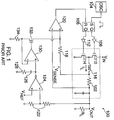
- FIG. 1 shows a prior art current-mode synchronous step-down switching regulator 100 that uses a current sensing element, e.g., current sense resistor 102, to monitor inductor current.
- Regulator 100 is typically used for DC-to-DC conversion of an unregulated supply voltage V IN (e.g., a battery) to a regulated output voltage V OUT , for driving a load R L , which, while simply shown as a resistor, may be, for example, a portable communication device or a computer.
- Regulator 100 operates typically as follows: at the beginning of a cycle, oscillator 104 sets latch 106 causing driver 108 to turn ON main switch MOSFET 110 and causing driver 112 to turn OFF synchronous switch MOSFET 114. This results in a voltage of approximately V IN -V OUT across inductor 116, which increases current through inductor 116. Inductor current I L flows through sense resistor 102 creating a differential sense voltage V SENSE , equal to the product of I L and sense resistor 102. When V SENSE exceeds the voltage across threshold-setting resistor 118, current comparator 120 trips and resets latch 106, which then causes driver 108 to turn OFF MOSFET 110 and driver 112 to turn ON MOSFET 114. This changes the voltage across inductor 116 to approximately -V OUT , causing inductor current I L to decrease until the next oscillator pulse sets latch 106.
- the threshold voltage across resistor 118 is set by the loop comprised of output resistor divider 122, error amplifier 124, compensation components 126 and 128, and voltage-to-current converter circuitry 130, 132, and 134. If the load current at V OUT increases, the resulting voltage drop at the inverting input of error amplifier 124 causes the outputs of error amplifier 124 and voltage-to-current converter circuitry 130 to increase, turning on transistor 132 and increasing the threshold voltage across resistor 118. Conversely, if the load current at V OUT decreases, the threshold voltage across resistor 118 decreases. Thus the threshold of current comparator 120 is continuously adjusted such that the average inductor current matches the load current.
- the current is limited to a value set by the maximum current comparator threshold. This value is set when the inductor current exceeds the threshold of the current comparator (i.e., V SENSE exceeds the voltage across resistor 118) for more than one oscillator cycle.
- the current comparator responds by providing a continuous reset signal to latch 106 that overrides the set input signal provided by the oscillator. This prevents main switch MOSFET 110 from turning ON, which causes the regulator to skip oscillator cycles.
- the loop (resistor divider 122, error amplifier 124, compensation components 126 and 128, and converter circuitry 130, 132, and 134) continues to cause cycles to be skipped until the inductor current falls below the maximum current comparator threshold.
- the ability to regulate current under short circuit conditions is an important advantage of current-mode switching regulators.
- a disadvantage of regulator 100 is that current sense resistor 102 causes additional dissipative losses in the regulator, thus reducing operating efficiency (which is the ratio of power provided by the regulator to the power provided to the regulator, a ratio of 1 being ideal).
- a further disadvantage is that, to prevent the dissipative losses from becoming excessive, the sense resistor must be a very low value -- typically in the range of 0.01 to 0.1 ohms. Such low value resistors are more difficult to manufacture than higher value resistors, resulting therefore in significantly higher manufacturing costs.
- the sense resistor is physically large and requires valuable printed circuit board area, which in portable product designs is often limited.
- Examples of current-mode synchronous switching regulators that employ current sense resistors are the Linear Technology LTC1148 and LTC1435, sold by Linear Technology Corporation, of Milpitas, California, and the Maxim MAX797, sold by Maxim Integrated Products, Inc., of Sunnyvale, California.
- Voltage-mode operation provides current limiting capabilities for short circuit protection by measuring the voltage drop across the conducting main switching element, which for MOSFET switches is known as "V DS sensing.” Such circuits do not otherwise require current sensing. For example, a voltage-mode switching regulator does not require current sensing during normal operation, because voltage-mode operation typically only relies on the output voltage to set the duty cycle.
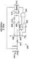
- FIG. 2 shows a prior art voltage-mode synchronous switching regulator 200 that uses V DS sensing for short circuit protection.
- Regulator 200 operates typically as follows: main switch MOSFET 202 and synchronous switch MOSFET 204 are coupled in series and to drivers 206 and 208, respectively. Inverter 210 ensures that MOSFET 204 is OFF when MOSFET 202 is ON and vice versa. During normal operation, only one parameter, output voltage V OUT , is used to set the regulator's duty cycle. This is accomplished by pulse-width-modulator 212, which varies the pulse width of output signal 214 in response to V OUT .
- pulse-width-modulator 212 normally responds by extending ON-portion 215 of signal 214 to its maximum value, the full period of signal 214. This causes the current flowing through MOSFET 202 and inductor 216 to increase without limit until failure.
- a fault loop is provided that includes AND gate 220, comparator 222, and threshold voltage 224.
- AND gate 220 which receives a second input from driver 206, ensures that the large V DS of MOSFET 202 is not misinterpreted as a fault when MOSFET 202 is OFF.
- regulator 200 is the compromised protection provided by V DS sensing. This protection is compromised because an accurate measurement of inductor current can only be made while main switch 202 is ON, but the extremely low duty cycles required to control the current during severe faults results in main switch 202 being OFF for substantially all of the cycle. Thus the time available to measure V DS approaches zero during short circuit conditions. Regulating short circuit current is therefore extremely difficult and often requires a complete shutdown to protect the regulator from destruction. Furthermore, additional means are required to resume normal operation after the short circuit is removed.
- V DS sensing examples include the LTC1430, sold by Linear Technology Corporation, and the Siliconix Si9150, sold by Siliconix Incorporated, of Santa Clara, California.
- a synchronous switching regulator circuit employing voltage-drop sensing.
- the regulator circuit includes an input terminal for coupling to a source of input supply voltage, an output terminal for coupling to a load, and output circuitry for supplying current to the load.
- the output circuitry is coupled to the input and output terminals and includes an inductor, a main switching element that causes current in the inductor to increase, and a synchronous switching element that conducts inductor current when the main switching element is non-conductive.
- the synchronous switching element is coupled to voltage-drop sensing circuitry, which measures the voltage drop across the synchronous switching element to generate current information. The voltage-drop sensing circuitry then provides that current information to control circuitry, which varies the regulator's duty cycle, if necessary, in response thereto.
- the present invention provides synchronous switching regulators that employ voltage-drop sensing circuitry to provide current information for controlling the duty cycle of the regulator. These regulators do not require a current sensing element, which is typically a resistor coupled in series with a load. The elimination of a current sensing element results advantageously in reduced dissipative losses and manufacturing complexity.
- the sensing circuitry senses the voltage drops across both the regulator's main and synchronous switching elements as each in turn conducts (i.e., are ON). The sensed voltage drops are then combined and converted into an analog waveform indicative of the inductor current. The waveform is then provided to control circuitry that responds by varying the ON-OFF states of the switching elements (i.e., the duty cycle of the regulator, which is the percentage of time that a switch is ON during a cycle of operation), thus regulating the amount of current supplied to a load.
- the ON-OFF states of the switching elements i.e., the duty cycle of the regulator, which is the percentage of time that a switch is ON during a cycle of operation
- sensing circuitry senses the voltage drop across the synchronous switching element as it conducts. When the sensed voltage drop exceeds a predetermined threshold, control circuitry reduces the regulator's duty cycle (i.e., keeps the main switching element OFF) to limit current while the output voltage is out of regulation.
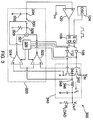
- Regulator 300 can be used, for example, to convert an unregulated DC supply voltage V IN to a regulated DC output voltage V OUT , for driving a load R LOAD , which, while simply shown as a resistor, may be, for example, a computer or a cordless telephone.
- Regulator 300 includes V DS sensing circuitry 320, output circuitry 340, and control circuitry that can include, for example, oscillator 104, current comparator 120, latch 106, and drivers 108 and 112.
- Output circuitry 340 includes inductor 346 and two serially coupled switching elements, main switch MOSFET 342 and synchronous switch MOSFET 344. These switching elements are driven out of phase with respect to each other to supply current at a regulated voltage to a load.
- FIG. 4 shows a waveform of regulator switch-voltage 400 taken at node 348 of FIG. 3.
- regulator 300 is similar to regulator 100 of FIG. 1, differences include the absence of a current sensing element (e.g., current sense resistor 102) and the manner in which inductor current is sensed in regulator 300. While regulator 100 relies on measuring the voltage across a current sense resistor, regulator 300 employs V DS sensing circuitry 320 to derive an analog waveform indicative of inductor current from the combined drain-to-source voltage drop measurements of the two MOSFET switching elements, taken as each in turn conducts. V DS sensing circuitry 320 eliminates the need for a current sensing element and thus provides regulator 300 with the advantages of current-mode operation without the disadvantages of a current sense element, particularly additional dissipative losses and a more costly manufacturing process.
- a current sensing element e.g., current sense resistor 102
- V DS sensing circuitry 320 operates generally as follows: when main switch MOSFET 342 is ON, it has a drain-to-source voltage drop V DS(342) , equal to the product of inductor current I L and the ON resistance of MOSFET 342 (R DS(ON)(342) ). By measuring V DS(342) of conducting MOSFET 342, sense amplifier 322 provides an analog waveform of I L related to V DS(342) by the constant R DS(ON)(342) . This waveform, indicated by reference numeral 500, is shown in FIG. 5.
- MOSFET 344 When MOSFET 342 turns OFF and synchronous switch MOSFET 344 turns ON, MOSFET 344 has a negative V DS(344) equal to the product of I L and R DS(ON)(344) . This permits I L to be sensed during the conduction of MOSFET 344 by measuring V DS(344) with sense amplifier 324, which then provides an analog waveform of I L related to V DS(344) by the constant -R DS(ON)(344) . This waveform, indicated by reference numeral 600, is shown in FIG. 6. Sense amplifiers 322 and 324 can also provide gain to amplify the analog inductor current waveforms.
- the drain-to-source voltages only provide valid current information while the MOSFETs are ON. For example, during conduction of MOSFET 342, no valid information about I L is provided by V DS(344) , because MOSFET 344 is OFF. Similarly, during conduction of MOSFET 344, no valid information about I L is provided by V DS(342) , because MOSFET 342 is OFF. In the time interval between the conduction of MOSFETs 342 and 344, neither V DS measurement provides valid information about I L , because both switches are OFF. During that time interval, blanking circuitry 326 (included as part of sensing circuitry 320) provides blanking signals to sense amplifiers 322 and 324 to disable their outputs.
- Blanking circuitry 326 which is known in the art, is controlled by the inputs and outputs of drivers 108 and 112. For example, sense amplifier 322 is immediately disabled upon receipt of a driver 108 input signal that turns MOSFET 342 OFF. Sense amplifier 322 is re-enabled by a driver 108 output signal after that signal has turned MOSFET 342 ON. Similarly, sense amplifier 324 is immediately disabled upon receipt of a driver 112 input signal that turns MOSFET 344 OFF, and is re-enabled by a driver 112 output signal after that signal has turned MOSFET 344 ON.
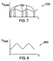
- the output waveforms of sense amplifiers 322 and 324 are fed to summation circuitry 327, which combines the two signals and outputs a single waveform at output 328, shown as summation signal 700 in FIG. 7.
- sense amplifiers 322 and 324 are transconductance amplifiers that output current.
- Summation circuitry 327 is then merely the connection of the two outputs to common resistor 329.
- sense amplifier 322 or 324 is enabled (i.e., its output is not blanked)
- the output current develops an output voltage across resistor 329 at node 328.
- summation circuitry 327 may be an op-amp circuit (known in the art and not shown) that combines the individual output voltages.
- the blanking of sense amplifiers 322 and 324 creates holes 702 in the waveform of summation signal 700. Holes 702 encompass the time intervals when both MOSFETs are OFF. To provide a smooth waveform to current comparator 120, holes 702 are filled at the peaks and troughs of waveform 700 by track-and-hold circuitry comprising switch 330 and capacitor 332. This circuitry holds the signal level that existed immediately prior to each blanking interval. After the blanking interval has ended, the output at node 334, shown as sense signal 800 in FIG. 8, is allowed to resume tracking of summation signal 700.
- Sense signal 800 is thus the reconstructed analog of the inductor current and is fed to current comparator 120. While the peak and trough hold-intervals represent lost information about the inductor current, this information is not necessary for proper operation of the regulator.
- Current comparator 120 determines when to turn OFF main switch MOSFET 342 during the rising portion of sense signal 800 and not the peak hold-interval. Similarly, current comparator 120 determines whether oscillator 104 is allowed to turn ON main switch MOSFET 342 (i.e., whether sense signal 800 has fallen below the current comparator threshold I TH before the next oscillator pulse) during the falling portion of sense signal 800 and not the trough hold-interval.
- V DS sensing circuitry 320 also senses the voltage drop of the synchronous MOSFET, in this case MOSFET 344, which is ON when MOSFET 342 is OFF.
- MOSFET 344 the current sense information available from MOSFET 344 trips comparator 120, causing comparator 120 to feed a continuous reset signal to latch 106. This overrides latch 106's set input which prevents main switch MOSFET 342 from turning ON, resulting in skipped cycles. Inductor current is then kept under control until the fault is corrected.
- FIG. 9 An exemplary embodiment of a voltage-mode synchronous switching regulator 900 employing voltage-drop sensing across the synchronous switch MOSFET in accordance with this invention is shown in FIG. 9. Because voltage-mode regulators are more susceptible to line and load transient signals than current-mode regulators, regulator 900 is advantageously used in applications which, for example, have a relatively constant input voltage (e.g., a 12 volt or 5 volt supply) and a relatively constant load current.
- a relatively constant input voltage e.g., a 12 volt or 5 volt supply
- Regulator 900 includes synchronous switch V DS sensing circuitry 920, output circuitry 940, and control circuitry that includes pulse-width-modulator 912 and drivers 906 and 908. While regulator 900 is similar to regulator 200 of FIG. 2, differences include V DS sensing of the synchronous switch MOSFET instead of the main switch MOSFET, and the limiting of the maximum duty cycle of the regulator to a predetermined value less than 100% in regulator 900.
- main switch MOSFET 902 and synchronous switch MOSFET 904 are driven by drivers 906 and 908, respectively, with inverter 910 ensuring that MOSFET 904 is OFF when MOSFET 902 is ON, and vice versa.
- Pulse-width-modulator 912 sets the regulator's duty cycle based on output voltage V OUT , with the limitation that the duty cycle cannot be greater than a predetermined value, such as, for example, 90%.
- a predetermined value such as, for example, 90%.
- the OFF-portion 917 of main switch MOSFET waveform 914 cannot be less than the difference between 100% and the predetermined maximum duty cycle (e.g., 10% for a 90% duty cycle).
- Limiting the maximum duty cycle ensures that driver 908 turns ON synchronous switch MOSFET 904 for at least a portion of each cycle, thus permitting V DS sensing circuitry 920 to obtain inductor current information. While such maximum duty cycle limitations may cause a step-down switching regulator to begin to lose regulation slightly earlier as input voltage V IN is reduced, there are no other undesirable operating effects on the regulator. Furthermore, if such a duty cycle limitation is unacceptable, it can be removed by combining the main switch MOSFET V DS sensing of regulator 200 with the synchronous switch MOSFET V DS sensing of regulator 900. The regulator therefore retains the advantage of improved short circuit protection without restricting its maximum duty cycle.
- V DS sensing circuitry 920 includes comparator 954, threshold voltage 950, blanking circuitry 926, and filter capacitor 952.
- the operation of comparator 954 and blanking circuitry 926 is similar to that of comparator 222 (of FIG. 2) and blanking circuitry 326 (of FIG. 3).
- Blanking circuitry 926 enables comparator 954 to monitor V DS(904) while synchronous switch MOSFET 904 is ON. If the inductor current causes V DS(904) to exceed threshold voltage 950, comparator 954 sinks current from filter capacitor 952 to cause the voltage at node 953, and, accordingly, the maximum allowed duty cycle (as shown in FIG. 10), to decrease.
- pulse-width-modulator 912 normally responds by extending the duty cycle to its maximum value, which, for example, may be 95%.
- V DS sensing circuitry 920 detects the increased inductor current and responds by reducing the duty cycle of main switch MOSFET 902, thus increasing the conduction time of synchronous switch MOSFET 904.
- accurate current sense information is still available from MOSFET 904.
- voltage-mode regulator 900 skips cycles as necessary to keep the inductor current under control (i.e., the voltage at node 953 is pulled down to a zero duty cycle as shown in FIG. 10).
- Regulators 300 and 900 therefore retain the advantages of regulating short circuit current, while avoiding both the disadvantages of invalid current information during low duty cycles as in regulator 200 and the disadvantages of a current sensing element as in regulator 100.
- regulators 300 and 900 are shown in a step-down configuration, the principles of the present invention can be applied to other synchronous regulator configurations, such as boost or buck-boost configurations, which are known in the art.
- the principles of the present invention can also be applied to other types of switching elements, such as, for example, bipolar transistors, where collector-to-emitter voltage drops are measured.
- the track-and-hold function of regulator 300 can be incorporated into sense amplifiers 322 and 324, thus allowing summation signal 700 to be applied directly to current comparator 120. Also, the gain of one or both current sense amplifiers can be adjusted to compensate for switching MOSFETs having mismatched R DS(ON) s.
Landscapes
- Engineering & Computer Science (AREA)
- Power Engineering (AREA)
- Dc-Dc Converters (AREA)
Abstract
Description
Claims (30)
- A synchronous switching regulator circuit for supplying current at a regulated voltage to a load, said regulator circuit comprising:an input terminal for coupling to a source of input supply voltage;an output terminal for coupling to said load;control circuitry for regulating the duty cycle of said regulator circuit;output circuitry coupled to said input terminal, to said output terminal, and to said control circuitry, said output circuitry comprising an inductor, a main switching element that causes current in said inductor to increase, and a synchronous switching element that conducts said inductor current when said main switching element is non-conductive; andvoltage-drop sensing circuitry coupled to said synchronous switching element and to said control circuitry for providing current information to said control circuitry.
- The regulator circuit of claim 1 wherein said voltage-drop sensing circuitry comprises:a sense amplifier coupled to said output circuitry; andblanking circuitry coupled to said sense amplifier and to said control circuitry.
- The circuit of claim 1 or 2 wherein said regulator circuit operates in current-mode.
- The regulator circuit of claim 3 wherein said voltage-drop sensing circuitry is also coupled to said main switching element.
- The regulator circuit of claim 4 wherein said voltage-drop sensing circuitry comprises:first and second sense amplifiers coupled to said output circuitry;blanking circuitry coupled to said first and second sense amplifiers and to said control circuitry; andsummation circuitry coupled to the outputs of said first and second sense amplifiers and to said control circuitry.
- The regulator circuit of claim 5 wherein said voltage-drop sensing circuitry further comprises track-and-hold circuitry coupled to said summation circuitry and to said control circuitry.
- The regulator circuit of claim 6 wherein said track-and-hold circuitry comprises:a switch coupled in series to said summation circuitry and to said control circuitry; anda capacitor coupled between said switch and said control circuitry to ground.
- The circuit of claim 5, 6 or 7 wherein said first and second sense amplifiers each comprises track-and-hold circuitry.
- The circuit of claim 5, 6, 7 or 8 wherein said first and second sense amplifiers each provides gain.
- The circuit of any one or claims 5 to 9 wherein said main and synchronous switching elements each comprise MOSFETs having mismatched RDS(ON)s, and at least one of said first and second sense amplifiers provides a gain that can compensate for said mismatched RDS(ON)s.
- The circuit of any one of claims 3 to 10 wherein said control circuitry comprises:an oscillator;a latch coupled to said oscillator and to said output circuitry; anda current comparator coupled to said latch and to said voltage-drop sensing circuitry.
- The regulator circuit or claim 1 or 2 wherein said regulator circuit operates in voltage-mode.
- The regulator circuit of claim 12 wherein the maximum duty cycle of said regulator circuit is less than 100% to permit valid voltage-drop sensing of said synchronous switching element during each cycle.
- The regulator circuit of claim 12 or 13, wherein said voltage-drop sensing circuitry comprises:a comparator coupled to said synchronous switching element and to said control circuitry; andblanking circuitry coupled to said control circuitry and to said comparator.
- The circuit of claim 12, 13 or 14 wherein said control circuitry comprises:a pulse-width-modulator coupled to said voltage-drop sensing circuitry and to said output terminal; anda plurality of drivers coupled to said pulse-width-modulator and to said output circuitry.
- The circuit of clan 12, 13, 14 or 15 wherein said synchronous switching element comprises a MOSFET.
- The circuit of any one of claims 12 to 16 wherein said synchronous switching element comprises a bipolar transistor.
- The regulator circuit of claims 1 to 17 wherein said main and synchronous switching elements comprise MOSFETs.
- The circuit of any one of claims 1 to 18 wherein said main and synchronous switching elements comprise bipolar transistors.
- The circuit of any one of claims 1 to 19 wherein said regulator circuit is in a step-down configuration.
- The circuit of any one of claims 1 to 20 wherein said regulator circuit is in a boost configuration.
- The circuit of any one of claims 1 to 21 wherein said regulator circuit is in a buck-boost configuration.
- A method of regulating current supplied to a load by a synchronous switching regulator, said regulator comprising control circuitry for controlling the regulator's duty cycle, output circuitry coupled to said control circuitry and to said load, said output circuitry comprising an inductor, a main switching element that causes current in said inductor to increase, a synchronous switching element that conducts said inductor current when said main switching element is non-conductive, and voltage-drop sensing circuitry coupled to said synchronous switching element and to said control circuitry, said method comprising the steps of:sensing the voltage drop across said synchronous switching element;deriving current information from said sensing; andvarying said duty cycle in response to said current information.
- The method of claim 23 wherein said step of sensing further comprises the step of:inhibiting said sensing step when said synchronous switching element is non-conducting.
- The method of claim 24 wherein said synchronous switching element is conducting during at least a portion of each cycle.
- The method of claim 23, 24 or 25 wherein said step of sensing further comprises the steps of:sensing the voltage drop across said main switching element; andsumming said sensed voltage drops of said main and synchronous switching elements.
- The method of claim 26 wherein said step of sensing the voltage drop across said main switching element further comprises the step of:inhibiting said sensing of said main switching element voltage drop when said main switching element is non-conducting.
- The method of claim 26 or 27 wherein said step of deriving comprises the steps of:deriving an analog signal waveform indicative of said current; andsmoothening said current analog signal waveform.
- A method of protecting a synchronous switching regulator from damage when a fault occurs, said regulator providing current to a load and comprising control circuitry for controlling the regulator's duty cycle, output circuitry coupled to said control circuitry and to said load, said output circuitry comprising an inductor, a main switching element that causes current in said inductor to increase, a synchronous switching element that conducts said inductor current when said main switching element is non-conductive, and voltage-drop sensing circuitry coupled to said synchronous switching element and to said control circuitry, said method comprising the steps of:sensing the voltage drop across said synchronous switching element;deriving a signal from said sensing indicative of an amount of current being supplied by said regulator; andreducing the duty cycle of said regulator if said signal exceeds a threshold.
- The method of claim 29 further comprising the step of:skipping cycles of said regulator until said threshold is no longer exceeded.
Applications Claiming Priority (2)
| Application Number | Priority Date | Filing Date | Title |
|---|---|---|---|
| US08/878,631 US5847554A (en) | 1997-06-13 | 1997-06-13 | Synchronous switching regulator which employs switch voltage-drop for current sensing |
| US878631 | 1997-06-13 |
Publications (3)
| Publication Number | Publication Date |
|---|---|
| EP0884746A2 true EP0884746A2 (en) | 1998-12-16 |
| EP0884746A3 EP0884746A3 (en) | 2000-08-02 |
| EP0884746B1 EP0884746B1 (en) | 2002-09-18 |
Family
ID=25372455
Family Applications (1)
| Application Number | Title | Priority Date | Filing Date |
|---|---|---|---|
| EP98110504A Expired - Lifetime EP0884746B1 (en) | 1997-06-13 | 1998-06-09 | Synchronous switching regulator which employs switch voltage-drop for current sensing |
Country Status (4)
| Country | Link |
|---|---|
| US (1) | US5847554A (en) |
| EP (1) | EP0884746B1 (en) |
| DE (1) | DE69807991T2 (en) |
| TW (1) | TW432789B (en) |
Cited By (7)
| Publication number | Priority date | Publication date | Assignee | Title |
|---|---|---|---|---|
| WO2000051226A1 (en) | 1999-02-23 | 2000-08-31 | Matsushita Electric Industrial Co., Ltd. | Switching regulator, dc/dc converter, and lsi system with switching regulator |
| GB2372586A (en) * | 1998-05-14 | 2002-08-28 | Intel Corp | Dynamic set point switching for CPU voltage regulator |
| EP1372252A1 (en) * | 2002-06-13 | 2003-12-17 | STMicroelectronics | Device and method for controlling a switching power source and switching power source provided with said device |
| US6724175B1 (en) | 2000-03-17 | 2004-04-20 | Fujitsu Limited | Power supply control device, power supply circuit, power supply control method, and electronic apparatus controlling output voltage thereof in accordance with a voltage detected across an on switching element |
| WO2005031955A1 (en) * | 2003-09-25 | 2005-04-07 | Koninklijke Philips Electronics N.V. | A switch mode power supply |
| EP2819288A1 (en) * | 2013-06-25 | 2014-12-31 | ST-Ericsson SA | Method of valley inductance current polarity detection in a pulse width modulated circuit with an inductive charge |
| CN104283421A (en) * | 2013-07-12 | 2015-01-14 | 凌力尔特有限公司 | Detecting faults in hot-swap applications |
Families Citing this family (92)
| Publication number | Priority date | Publication date | Assignee | Title |
|---|---|---|---|---|
| US5973485A (en) * | 1995-06-28 | 1999-10-26 | Dell Usa, L.P. | Method and apparatus for a multiple stage sequential synchronous regulator |
| US5945820A (en) * | 1997-02-06 | 1999-08-31 | The Board Of Trustees Of The Leland Stanford Junior University | DC-DC switching regulator with switching rate control |
| SE510611C2 (en) * | 1997-08-06 | 1999-06-07 | Ericsson Telefon Ab L M | BUCK-BOOST VOLTAGE REGULATOR |
| US6025705A (en) * | 1997-12-24 | 2000-02-15 | Intel Corporation | DC-to-DC converter |
| US6160388A (en) * | 1997-12-30 | 2000-12-12 | Texas Instruments Incorporated | Sensing of current in a synchronous-buck power stage |
| US6069471A (en) * | 1998-05-14 | 2000-05-30 | Intel Corporation | Dynamic set point switching regulator |
| US6107787A (en) * | 1998-10-29 | 2000-08-22 | Methode Electronics, Inc. | Automobile dashboard light control |
| JP2000193687A (en) | 1998-12-25 | 2000-07-14 | Toyota Autom Loom Works Ltd | Current detection circuit and dc/dc converter provided with current detection circuit |
| FR2791443B1 (en) * | 1999-03-23 | 2001-12-28 | Valeo Vision | VOLTAGE REGULATION SYSTEM FOR LOADS ON-BOARD IN A MOTOR VEHICLE |
| US6175221B1 (en) | 1999-08-31 | 2001-01-16 | Micron Technology, Inc. | Frequency sensing NMOS voltage regulator |
| US6166528A (en) * | 1999-11-02 | 2000-12-26 | Fairchild Semiconductor Corporation | Lossless current sensing in buck converters working with low duty cycles and high clock frequencies |
| TW512578B (en) | 2000-03-21 | 2002-12-01 | Int Rectifier Corp | Inductor current synthesizer for switching power supplies |
| JP3619494B2 (en) * | 2000-03-22 | 2005-02-09 | インターナショナル・レクチファイヤー・コーポレーション | Inductor current synthesizer for switching power supply |
| US6301139B1 (en) | 2000-04-06 | 2001-10-09 | Power-One, Inc. | Self-driven synchronous rectifier circuit for non-optimal reset secondary voltage |
| US6323703B1 (en) * | 2000-05-04 | 2001-11-27 | Exar Corporation | Indirect output current sensing |
| DE10043482A1 (en) * | 2000-09-04 | 2002-03-14 | Infineon Technologies Ag | Current Mode Switching Regulators |
| JP3617433B2 (en) * | 2000-09-05 | 2005-02-02 | 株式会社デンソー | Driving circuit |
| US6813173B2 (en) * | 2000-10-26 | 2004-11-02 | 02Micro International Limited | DC-to-DC converter with improved transient response |
| US6459602B1 (en) * | 2000-10-26 | 2002-10-01 | O2 Micro International Limited | DC-to-DC converter with improved transient response |
| US6404657B1 (en) | 2000-11-20 | 2002-06-11 | Maxim Integrated Products | Method to synchronize multiple switching regulators in out of phase mode without PLL |
| US6531853B2 (en) * | 2000-11-21 | 2003-03-11 | Rohm Co., Ltd. | DC-DC converter |
| DE10101744C1 (en) * | 2001-01-16 | 2002-08-08 | Siemens Ag | Electronic switching device and operating method |
| US6545886B1 (en) * | 2001-05-05 | 2003-04-08 | Anthony J. Ireland | Power conditioning for model railroad control decoders |
| US6683441B2 (en) * | 2001-11-26 | 2004-01-27 | Analog Devices, Inc. | Multi-phase switching regulator |
| US6522113B1 (en) * | 2001-12-06 | 2003-02-18 | Texas Instruments Incorporated | Synchronous coupled inductor switching regulator with improved output regulation |
| GB0200027D0 (en) * | 2002-01-02 | 2002-02-13 | Bae Systems Plc | Improvements relating to operation of a current controller |
| GB0200024D0 (en) * | 2002-01-02 | 2002-02-13 | Bae Systems Plc | A switching circuit and a method of operation thereof |
| GB0200030D0 (en) * | 2002-01-02 | 2002-02-13 | Bae Systems Plc | A switching circuit and a method of operation thereof |
| US7005835B2 (en) * | 2002-06-28 | 2006-02-28 | Microsemi Corp. | Method and apparatus for load sharing in a multiphase switching power converter |
| US6965219B2 (en) * | 2002-06-28 | 2005-11-15 | Microsemi Corporation | Method and apparatus for auto-interleaving synchronization in a multiphase switching power converter |
| US6943535B1 (en) | 2002-10-17 | 2005-09-13 | Analog Devices, Inc. | Multiple-phase DC-DC converter topology |
| US6906502B2 (en) | 2002-11-14 | 2005-06-14 | Fyre Storm, Inc. | Method for regulating an output voltage of a power coverter |
| TW588489B (en) * | 2002-11-14 | 2004-05-21 | Richtek Technology Corp | Over-current protection apparatus and method of switching type regulator |
| US7062665B2 (en) * | 2002-12-18 | 2006-06-13 | Intel Corporation | Control of voltage regulator thermal condition |
| US6940261B1 (en) * | 2003-03-19 | 2005-09-06 | Linear Technology Corporation | Circuits and methods for providing multiple phase switching regulators which employ the input capacitor voltage signal for current sensing |
| TWM258493U (en) * | 2003-06-26 | 2005-03-01 | O2Micro Inc | DC-to-DC converter with improved transient response |
| US6861830B1 (en) * | 2003-10-22 | 2005-03-01 | Aimtron Technology Corp. | Method of improving transient noise of a switching DC-to-DC converter with multiple output voltages |
| US7019507B1 (en) | 2003-11-26 | 2006-03-28 | Linear Technology Corporation | Methods and circuits for programmable current limit protection |
| EP1587208A1 (en) * | 2004-04-14 | 2005-10-19 | Infineon Technologies AG | Buck converter with low loss current measurement |
| US6970339B2 (en) * | 2004-04-27 | 2005-11-29 | Texas Instruments Incorporated | Current limit protection scheme for PWM buck converter with synchronous rectifier |
| TWI235541B (en) * | 2004-06-25 | 2005-07-01 | Anpec Electronics Corp | Current detection circuit and method for use in DC-to-DC converter |
| DE102004037543B4 (en) * | 2004-08-03 | 2017-02-16 | Infineon Technologies Ag | Device for protecting a half-bridge circuit arrangement from a short circuit across a load |
| DE602004006623T2 (en) * | 2004-08-27 | 2008-01-17 | Infineon Technologies Ag | Control circuit for current mode downconverters |
| US7199560B2 (en) * | 2004-11-05 | 2007-04-03 | Linear Technology Corporation | Switch-mode power supply voltage regulator and methodology |
| JP2006262646A (en) * | 2005-03-17 | 2006-09-28 | Ricoh Co Ltd | Step-down switching regulator |
| US7919952B1 (en) | 2005-03-21 | 2011-04-05 | Microsemi Corporation | Automatic gain control technique for current monitoring in current-mode switching regulators |
| JP4347249B2 (en) * | 2005-03-31 | 2009-10-21 | 富士通マイクロエレクトロニクス株式会社 | DC-DC converter, control circuit for DC-DC converter, and control method for DC-DC converter |
| US20060227478A1 (en) * | 2005-04-11 | 2006-10-12 | Linear Technology Corporation | Inrush current control system with soft start circuit and method |
| US7425819B2 (en) * | 2005-06-16 | 2008-09-16 | Microsemi Corporation | Slope compensation circuit |
| US7579818B2 (en) * | 2005-07-28 | 2009-08-25 | Semiconductor Components Industries, L.L.C. | Current regulator and method therefor |
| JP4421534B2 (en) * | 2005-09-05 | 2010-02-24 | 富士通マイクロエレクトロニクス株式会社 | DC-DC converter and control method thereof, and switching regulator and control method thereof |
| TWI313958B (en) * | 2006-03-22 | 2009-08-21 | Anpec Electronics Corp | Switching regulator capable of compensating output errors |
| TWI313959B (en) * | 2006-03-22 | 2009-08-21 | Anpec Electronics Corp | Switching regulator capable of raising system stability by virtual ripple |
| US7902805B2 (en) * | 2006-04-03 | 2011-03-08 | Texas Instruments Deutschland Gmbh | Self-oscillating DC-DC buck converter with zero hysteresis |
| US20070236191A1 (en) * | 2006-04-11 | 2007-10-11 | Advanced Analogic Technologies, Inc. | Boost Regulator with Integrated Load Switch |
| US7593200B2 (en) * | 2006-08-15 | 2009-09-22 | International Rectifier Corporation | Buck converter fault detection method |
| JP2008154419A (en) * | 2006-12-20 | 2008-07-03 | Ricoh Co Ltd | Switching regulator and semiconductor device constituting same |
| US7633321B2 (en) * | 2007-07-24 | 2009-12-15 | Infineon Technologies Ag | Driver circuit; electronic circuit having driver circuit and corresponding method |
| US20090128111A1 (en) * | 2007-11-19 | 2009-05-21 | Shang-Yu Chang Chien | Reverse current protection apparatus for a synchronous switching voltage converter |
| US7843146B2 (en) * | 2008-01-28 | 2010-11-30 | Global Mixed-Mode Technology Inc. | LED dimming control circuit |
| US8587974B2 (en) * | 2008-03-25 | 2013-11-19 | Ragnar Jonsson | Method and device for increasing control accuracy in a PWM system |
| US8232784B2 (en) * | 2008-04-01 | 2012-07-31 | O2Micro, Inc | Circuits and methods for current sensing |
| EP2330728A4 (en) * | 2008-09-22 | 2014-11-26 | Fujitsu Ltd | Power control circuit, power supply unit, power supply system, and power controller control method |
| US9203301B2 (en) | 2010-06-23 | 2015-12-01 | Volterra Semiconductor Corporation | Feedback for controlling the switching frequency of a voltage regulator |
| US9397571B2 (en) | 2010-06-23 | 2016-07-19 | Volterra Semiconductor Corporation | Controlled delivery of a charging current to a boost capacitor of a voltage regulator |
| US9570985B2 (en) * | 2010-07-02 | 2017-02-14 | Renesas Electronics America Inc. | Intelligent gate drive voltage generator |
| US8629669B2 (en) | 2010-07-27 | 2014-01-14 | Volterra Semiconductor Corporation | Sensing and feedback in a current mode control voltage regulator |
| US20120229107A1 (en) * | 2011-03-11 | 2012-09-13 | Intersil Americas Inc. | System and method for current sensing within a voltage regulator |
| TW201246769A (en) * | 2011-05-10 | 2012-11-16 | Hon Hai Prec Ind Co Ltd | Buck converter |
| US8610609B2 (en) * | 2011-09-09 | 2013-12-17 | Mstar Semiconductor, Inc. | NMOS buffer for high-speed low-resolution current steering digital-to-analog converters |
| US8629668B2 (en) | 2011-09-19 | 2014-01-14 | Eta Semiconductor Inc. | Multi-phase synthetic ripple power converter |
| US8643351B2 (en) * | 2011-12-28 | 2014-02-04 | Monolithic Power Systems, Inc. | Switching mode power supply and the method thereof |
| US9195246B2 (en) | 2012-02-09 | 2015-11-24 | Volterra Semiconductor Corporation | Virtual output voltage sensing for feed-forward control of a voltage regulator |
| US9281747B2 (en) | 2012-06-26 | 2016-03-08 | Volterra Semiconductor Corporation | Voltage regulator control using information from a load |
| US8878509B2 (en) * | 2012-08-17 | 2014-11-04 | St-Ericsson Sa | Current-mode controller for step-down (buck) converter |
| US8823345B2 (en) | 2012-10-19 | 2014-09-02 | Linear Technology Corporation | Magnetic field cancellation in switching regulators |
| JP6034132B2 (en) * | 2012-10-24 | 2016-11-30 | 株式会社ソニー・インタラクティブエンタテインメント | DC / DC converter and game machine using the same |
| KR102038119B1 (en) * | 2012-11-09 | 2019-10-29 | 삼성전자주식회사 | Electronic Apparatus, Apparatus for Providing Power and Method for Providing Power |
| EP2730931B1 (en) | 2012-11-12 | 2015-08-26 | ST-Ericsson SA | Absolute value current-sensing circuit for step-down DC-to-DC converters with integrated power stage |
| US9048734B2 (en) * | 2013-03-01 | 2015-06-02 | Analog Devices Global | Negative current protection system for low side switching converter FET |
| US20140253080A1 (en) * | 2013-03-11 | 2014-09-11 | Qualcomm Incorporated | Method and apparatus for advanced pulse skipping control in buck regulators |
| DE102013208813A1 (en) * | 2013-05-14 | 2014-11-20 | Robert Bosch Gmbh | Control of a half bridge |
| DE102014003405B4 (en) * | 2014-03-07 | 2021-10-21 | Elmos Semiconductor Se | Down-converting LED driver with a mean-value-based control concept for use in vehicles |
| DE102014017308B4 (en) | 2014-03-07 | 2021-01-28 | Elmos Semiconductor Se | Down-converting LED driver with a mean value-based control concept for use in vehicles with a minimum switch-off period |
| DE102014205844A1 (en) * | 2014-03-28 | 2015-10-01 | Robert Bosch Gmbh | Device and method for reducing switching losses in power transistors |
| EP3188351B1 (en) | 2015-12-28 | 2020-12-02 | Rohm Co., Ltd. | Buck converter with duty ratio based fault detection |
| JP6594199B2 (en) * | 2015-12-28 | 2019-10-23 | ローム株式会社 | Switching regulator |
| US10224812B1 (en) * | 2017-10-13 | 2019-03-05 | Infineon Technologies Austria Ag | Sensing network mismatch compensation for switching voltage regulator with input voltage and current sensing |
| US10509426B2 (en) * | 2018-05-02 | 2019-12-17 | Analog Devices Global Unlimited Company | Methods and circuits for controlling and/or reducing current leakage during a low-power or inactive mode |
| CN110504830B (en) * | 2019-08-19 | 2021-02-23 | 东莞市长工微电子有限公司 | Reconstruction circuit and reconstruction method of inductive current |
| US11811314B2 (en) * | 2020-12-30 | 2023-11-07 | Texas Instruments Incorporated | Multi-mode power converter with programmable control |
| US20230396141A1 (en) * | 2022-06-02 | 2023-12-07 | Psemi Corporation | Circuits and methods for generating a continuous current sense signal |
Citations (3)
| Publication number | Priority date | Publication date | Assignee | Title |
|---|---|---|---|---|
| EP0617501A1 (en) * | 1993-03-23 | 1994-09-28 | Linear Technology Corporation | Control circuit and method for maintaining high efficiency over broad current ranges in a switching regulator circuit |
| US5359277A (en) * | 1993-01-05 | 1994-10-25 | Alliedsignal Inc. | Low distortion alternating current output active power factor correction circuit using bi-directional bridge rectifier and bi-directional switching regulator |
| US5404094A (en) * | 1994-03-18 | 1995-04-04 | Holophane Lighting, Inc. | Wide input power supply and method of converting therefor |
Family Cites Families (4)
| Publication number | Priority date | Publication date | Assignee | Title |
|---|---|---|---|---|
| US4823070A (en) * | 1986-11-18 | 1989-04-18 | Linear Technology Corporation | Switching voltage regulator circuit |
| US5479090A (en) * | 1993-11-24 | 1995-12-26 | Raytheon Company | Power converter having optimal dynamic operation |
| US5414341A (en) * | 1993-12-07 | 1995-05-09 | Benchmarq Microelectronics, Inc. | DC-DC converter operable in an asyncronous or syncronous or linear mode |
| US5552695A (en) * | 1994-03-22 | 1996-09-03 | Linear Technology Corporation | Synchronously rectified buck-flyback DC to DC power converter |
-
1997
- 1997-06-13 US US08/878,631 patent/US5847554A/en not_active Expired - Lifetime
-
1998
- 1998-06-09 DE DE69807991T patent/DE69807991T2/en not_active Expired - Lifetime
- 1998-06-09 EP EP98110504A patent/EP0884746B1/en not_active Expired - Lifetime
- 1998-06-12 TW TW087109392A patent/TW432789B/en not_active IP Right Cessation
Patent Citations (3)
| Publication number | Priority date | Publication date | Assignee | Title |
|---|---|---|---|---|
| US5359277A (en) * | 1993-01-05 | 1994-10-25 | Alliedsignal Inc. | Low distortion alternating current output active power factor correction circuit using bi-directional bridge rectifier and bi-directional switching regulator |
| EP0617501A1 (en) * | 1993-03-23 | 1994-09-28 | Linear Technology Corporation | Control circuit and method for maintaining high efficiency over broad current ranges in a switching regulator circuit |
| US5404094A (en) * | 1994-03-18 | 1995-04-04 | Holophane Lighting, Inc. | Wide input power supply and method of converting therefor |
Cited By (17)
| Publication number | Priority date | Publication date | Assignee | Title |
|---|---|---|---|---|
| GB2372586A (en) * | 1998-05-14 | 2002-08-28 | Intel Corp | Dynamic set point switching for CPU voltage regulator |
| GB2372586B (en) * | 1998-05-14 | 2002-10-16 | Intel Corp | Dynamic set point switching |
| EP1079507A4 (en) * | 1999-02-23 | 2008-07-02 | Matsushita Electric Ind Co Ltd | Switching regulator, dc/dc converter, and lsi system with switching regulator |
| EP1079507A1 (en) * | 1999-02-23 | 2001-02-28 | Matsushita Electric Industrial Co., Ltd. | Switching regulator, dc/dc converter, and lsi system with switching regulator |
| WO2000051226A1 (en) | 1999-02-23 | 2000-08-31 | Matsushita Electric Industrial Co., Ltd. | Switching regulator, dc/dc converter, and lsi system with switching regulator |
| EP2110935A3 (en) * | 1999-02-23 | 2010-01-20 | Panasonic Corporation | DC/DC Converter |
| EP2110935A2 (en) | 1999-02-23 | 2009-10-21 | Panasonic Corporation | DC/DC Converter |
| US6724175B1 (en) | 2000-03-17 | 2004-04-20 | Fujitsu Limited | Power supply control device, power supply circuit, power supply control method, and electronic apparatus controlling output voltage thereof in accordance with a voltage detected across an on switching element |
| EP1134880A3 (en) * | 2000-03-17 | 2004-08-25 | Fujitsu Limited | Power supply control device and method, power supply control method, and electronic apparatus |
| EP1372252A1 (en) * | 2002-06-13 | 2003-12-17 | STMicroelectronics | Device and method for controlling a switching power source and switching power source provided with said device |
| US6867571B2 (en) | 2002-06-13 | 2005-03-15 | Stmicroelectronics S.A. | Device and method for controlling a switching power supply and corresponding switching power supply |
| FR2841061A1 (en) * | 2002-06-13 | 2003-12-19 | St Microelectronics Sa | DEVICE AND METHOD FOR CONTROLLING A CUT-OUT POWER SOURCE AND CUT-OUT POWER SOURCE PROVIDED WITH SUCH A STEERING DEVICE |
| WO2005031955A1 (en) * | 2003-09-25 | 2005-04-07 | Koninklijke Philips Electronics N.V. | A switch mode power supply |
| EP2819288A1 (en) * | 2013-06-25 | 2014-12-31 | ST-Ericsson SA | Method of valley inductance current polarity detection in a pulse width modulated circuit with an inductive charge |
| US9459311B2 (en) | 2013-06-25 | 2016-10-04 | Stmicroelectronics International N.V. | Method of valley inductance current polarity detection in a pulse width modulated circuit with an inductive charge |
| CN104283421A (en) * | 2013-07-12 | 2015-01-14 | 凌力尔特有限公司 | Detecting faults in hot-swap applications |
| CN104283421B (en) * | 2013-07-12 | 2018-08-10 | 凌力尔特有限公司 | Fault detect in hot plug application |
Also Published As
| Publication number | Publication date |
|---|---|
| US5847554A (en) | 1998-12-08 |
| DE69807991T2 (en) | 2003-01-23 |
| EP0884746A3 (en) | 2000-08-02 |
| DE69807991D1 (en) | 2002-10-24 |
| TW432789B (en) | 2001-05-01 |
| EP0884746B1 (en) | 2002-09-18 |
Similar Documents
| Publication | Publication Date | Title |
|---|---|---|
| EP0884746B1 (en) | Synchronous switching regulator which employs switch voltage-drop for current sensing | |
| US7064531B1 (en) | PWM buck regulator with LDO standby mode | |
| US10218265B2 (en) | State space-based multi-level voltage regulator system | |
| US6343026B1 (en) | Current limit circuit for interleaved converters | |
| US7019507B1 (en) | Methods and circuits for programmable current limit protection | |
| US8598860B2 (en) | Transient recovery circuit for switching devices | |
| US7919952B1 (en) | Automatic gain control technique for current monitoring in current-mode switching regulators | |
| CA2576705C (en) | Switching voltage regulator with low current trickle mode | |
| US6717389B1 (en) | Method and apparatus for current controlled transient reduction in a voltage regulator | |
| US7868483B2 (en) | Power management systems with current sensors | |
| US8866460B2 (en) | Dynamic dropout control of a power supply | |
| US6130526A (en) | Voltage regulator with wide control bandwidth | |
| EP2602922A2 (en) | Power management system for Universal Serial Bus | |
| JPH10225105A (en) | Dc-dc converter | |
| US20100264895A1 (en) | Power-supply controller | |
| US6249411B1 (en) | Over-voltage protection circuit and method for preventing system shutdown in a power system employing multiple power supplies | |
| CN212850271U (en) | Switched mode power supply | |
| US10291120B2 (en) | Boost DC-DC converter having digital control and reference PWM generators | |
| US7023191B2 (en) | Voltage regulator with adjustable output impedance | |
| US20220393593A1 (en) | Control circuit of dc/dc converter, power supply circuit, and electronic device | |
| US7239533B2 (en) | DC power supply apparatus | |
| CN113114038A (en) | Method and apparatus for adjusting a voltage regulation set point of a power converter | |
| US10700518B2 (en) | Constant current limiting protection for series coupled power supplies | |
| US20220247301A1 (en) | Load regulation | |
| US11456667B2 (en) | Constant ripple injection circuit for switching converter |
Legal Events
| Date | Code | Title | Description |
|---|---|---|---|
| PUAI | Public reference made under article 153(3) epc to a published international application that has entered the european phase |
Free format text: ORIGINAL CODE: 0009012 |
|
| AK | Designated contracting states |
Kind code of ref document: A2 Designated state(s): CH DE FR GB IT LI |
|
| AX | Request for extension of the european patent |
Free format text: AL;LT;LV;MK;RO;SI |
|
| PUAL | Search report despatched |
Free format text: ORIGINAL CODE: 0009013 |
|
| AK | Designated contracting states |
Kind code of ref document: A3 Designated state(s): AT BE CH CY DE DK ES FI FR GB GR IE IT LI LU MC NL PT SE |
|
| AX | Request for extension of the european patent |
Free format text: AL;LT;LV;MK;RO;SI |
|
| 17P | Request for examination filed |
Effective date: 20010102 |
|
| AKX | Designation fees paid |
Free format text: CH DE FR GB IT LI |
|
| GRAG | Despatch of communication of intention to grant |
Free format text: ORIGINAL CODE: EPIDOS AGRA |
|
| 17Q | First examination report despatched |
Effective date: 20011001 |
|
| GRAG | Despatch of communication of intention to grant |
Free format text: ORIGINAL CODE: EPIDOS AGRA |
|
| GRAH | Despatch of communication of intention to grant a patent |
Free format text: ORIGINAL CODE: EPIDOS IGRA |
|
| GRAH | Despatch of communication of intention to grant a patent |
Free format text: ORIGINAL CODE: EPIDOS IGRA |
|
| GRAA | (expected) grant |
Free format text: ORIGINAL CODE: 0009210 |
|
| AK | Designated contracting states |
Kind code of ref document: B1 Designated state(s): CH DE FR GB IT LI |
|
| REG | Reference to a national code |
Ref country code: GB Ref legal event code: FG4D |
|
| REG | Reference to a national code |
Ref country code: CH Ref legal event code: EP |
|
| REF | Corresponds to: |
Ref document number: 69807991 Country of ref document: DE Date of ref document: 20021024 |
|
| REG | Reference to a national code |
Ref country code: CH Ref legal event code: NV Representative=s name: BOVARD AG PATENTANWAELTE |
|
| ET | Fr: translation filed | ||
| PLBE | No opposition filed within time limit |
Free format text: ORIGINAL CODE: 0009261 |
|
| STAA | Information on the status of an ep patent application or granted ep patent |
Free format text: STATUS: NO OPPOSITION FILED WITHIN TIME LIMIT |
|
| 26N | No opposition filed |
Effective date: 20030619 |
|
| REG | Reference to a national code |
Ref country code: CH Ref legal event code: PFA Owner name: LINEAR TECHNOLOGY CORPORATION Free format text: LINEAR TECHNOLOGY CORPORATION#1630 MCCARTHY BOULEVARD#MILPITAS CALIFORNIA 95035 (US) -TRANSFER TO- LINEAR TECHNOLOGY CORPORATION#1630 MCCARTHY BOULEVARD#MILPITAS CALIFORNIA 95035 (US) |
|
| REG | Reference to a national code |
Ref country code: FR Ref legal event code: PLFP Year of fee payment: 19 |
|
| REG | Reference to a national code |
Ref country code: FR Ref legal event code: PLFP Year of fee payment: 20 |
|
| PGFP | Annual fee paid to national office [announced via postgrant information from national office to epo] |
Ref country code: FR Payment date: 20170627 Year of fee payment: 20 Ref country code: GB Payment date: 20170627 Year of fee payment: 20 Ref country code: CH Payment date: 20170627 Year of fee payment: 20 |
|
| PGFP | Annual fee paid to national office [announced via postgrant information from national office to epo] |
Ref country code: IT Payment date: 20170622 Year of fee payment: 20 |
|
| PGFP | Annual fee paid to national office [announced via postgrant information from national office to epo] |
Ref country code: DE Payment date: 20170628 Year of fee payment: 20 |
|
| REG | Reference to a national code |
Ref country code: DE Ref legal event code: R071 Ref document number: 69807991 Country of ref document: DE |
|
| REG | Reference to a national code |
Ref country code: CH Ref legal event code: PL |
|
| REG | Reference to a national code |
Ref country code: GB Ref legal event code: PE20 Expiry date: 20180608 |
|
| PG25 | Lapsed in a contracting state [announced via postgrant information from national office to epo] |
Ref country code: GB Free format text: LAPSE BECAUSE OF EXPIRATION OF PROTECTION Effective date: 20180608 |
|
| REG | Reference to a national code |
Ref country code: GB Ref legal event code: 732E Free format text: REGISTERED BETWEEN 20210930 AND 20211006 |