EP0682401A1 - Limiting device for the output voltage slope of a self-commutated converter - Google Patents
Limiting device for the output voltage slope of a self-commutated converter Download PDFInfo
- Publication number
- EP0682401A1 EP0682401A1 EP95106488A EP95106488A EP0682401A1 EP 0682401 A1 EP0682401 A1 EP 0682401A1 EP 95106488 A EP95106488 A EP 95106488A EP 95106488 A EP95106488 A EP 95106488A EP 0682401 A1 EP0682401 A1 EP 0682401A1
- Authority
- EP
- European Patent Office
- Prior art keywords
- induction machine
- capacitance network
- voltage
- strands
- current
- Prior art date
- Legal status (The legal status is an assumption and is not a legal conclusion. Google has not performed a legal analysis and makes no representation as to the accuracy of the status listed.)
- Granted
Links
Images
Classifications
-
- H—ELECTRICITY
- H02—GENERATION; CONVERSION OR DISTRIBUTION OF ELECTRIC POWER
- H02M—APPARATUS FOR CONVERSION BETWEEN AC AND AC, BETWEEN AC AND DC, OR BETWEEN DC AND DC, AND FOR USE WITH MAINS OR SIMILAR POWER SUPPLY SYSTEMS; CONVERSION OF DC OR AC INPUT POWER INTO SURGE OUTPUT POWER; CONTROL OR REGULATION THEREOF
- H02M7/00—Conversion of ac power input into dc power output; Conversion of dc power input into ac power output
- H02M7/42—Conversion of dc power input into ac power output without possibility of reversal
- H02M7/44—Conversion of dc power input into ac power output without possibility of reversal by static converters
- H02M7/48—Conversion of dc power input into ac power output without possibility of reversal by static converters using discharge tubes with control electrode or semiconductor devices with control electrode
- H02M7/53—Conversion of dc power input into ac power output without possibility of reversal by static converters using discharge tubes with control electrode or semiconductor devices with control electrode using devices of a triode or transistor type requiring continuous application of a control signal
- H02M7/537—Conversion of dc power input into ac power output without possibility of reversal by static converters using discharge tubes with control electrode or semiconductor devices with control electrode using devices of a triode or transistor type requiring continuous application of a control signal using semiconductor devices only, e.g. single switched pulse inverters
- H02M7/5387—Conversion of dc power input into ac power output without possibility of reversal by static converters using discharge tubes with control electrode or semiconductor devices with control electrode using devices of a triode or transistor type requiring continuous application of a control signal using semiconductor devices only, e.g. single switched pulse inverters in a bridge configuration
-
- H—ELECTRICITY
- H02—GENERATION; CONVERSION OR DISTRIBUTION OF ELECTRIC POWER
- H02M—APPARATUS FOR CONVERSION BETWEEN AC AND AC, BETWEEN AC AND DC, OR BETWEEN DC AND DC, AND FOR USE WITH MAINS OR SIMILAR POWER SUPPLY SYSTEMS; CONVERSION OF DC OR AC INPUT POWER INTO SURGE OUTPUT POWER; CONTROL OR REGULATION THEREOF
- H02M1/00—Details of apparatus for conversion
- H02M1/12—Arrangements for reducing harmonics from ac input or output
-
- H—ELECTRICITY
- H02—GENERATION; CONVERSION OR DISTRIBUTION OF ELECTRIC POWER
- H02P—CONTROL OR REGULATION OF ELECTRIC MOTORS, ELECTRIC GENERATORS OR DYNAMO-ELECTRIC CONVERTERS; CONTROLLING TRANSFORMERS, REACTORS OR CHOKE COILS
- H02P5/00—Arrangements specially adapted for regulating or controlling the speed or torque of two or more electric motors
- H02P5/74—Arrangements specially adapted for regulating or controlling the speed or torque of two or more electric motors controlling two or more ac dynamo-electric motors
Definitions
- the present invention is in the field of frequency converters or inverters, which have been increasingly used for speed control of induction machines for several years. So-called U inverters with a DC voltage intermediate circuit are predominantly used. The latter forms a DC voltage from the normally constant mains voltage. This is switched in the inverter by means of power semiconductor switches, whereby the desired three-phase three-phase network with variable voltage and frequency is provided.
- the invention now relates to a device for limiting the rate of change of the output-side voltage of a converter which is self-controlled via a DC voltage intermediate circuit and which has output terminals for the connection of at least one induction machine and an inductance arranged between each output terminal and the at least one induction machine.
- the inductors are so-called current rise limiting chokes, which are followed by three diode branches, each with two diodes.
- the current rise limiting chokes are each connected to the line piece connecting the cathode connection of one diode to the anode connection of the other diode of a diode branch.
- this known device can noticeably reduce some of the problems listed above, in particular the stress on the insulation of the connected induction machine due to steep voltage pulses or the stress on the power semiconductors due to the connecting cable, it is practically ineffective with regard to other problems. This is due to the fact that this device essentially only acts on the symmetrical voltages, that is to say on the voltages between the live lines, and practically does not influence the asymmetrical voltages.
- the invention is intended to provide a device of the type mentioned which acts both on symmetrical and on asymmetrical interference voltages and thereby eliminates or at least significantly reduces the problems mentioned at the outset.
- the device according to the invention reduces the rising and falling edges of the voltage pulses generated by the converter, as a result of which the problems with the stress on the insulation of the induction machines are reduced to a reasonable degree. At the same time, it affects the asymmetrical voltages with respect to the earth potential, whereby the disturbances caused by these asymmetrical voltages are also eliminated or at least largely reduced.
- inverter or frequency converter 1 provided for speed count control of induction machines, which is connected to a DC link 2 symbolized by a capacitor. This is fed by a mains rectifier (not shown) connected to the supply network with a usually constant voltage and constant frequency.
- the converter 1 switches the DC voltage of the DC voltage intermediate circuit 2 by means of power semiconductor switches and provides the desired three-phase three-phase network with variable frequency and voltage at its output terminals 3 for the connected induction machines 4 (e.g. motors M). If this description refers to induction machines or induction machines, then both, both a single machine and a machine group, are meant.
- FIG. 2 shows a theoretically possible variant that also largely reduces the asymmetrical voltages and thus could largely eliminate or reduce all the disadvantageous properties of the known converters discussed above.
- two capacitances C connected in a star are connected to each inductance L, and the star points are each connected to one pole of the intermediate circuit voltage of the converter 1.
- this circuit both sinusoidal, symmetrical voltages can be generated and the asymmetrical voltages can be limited in terms of their rise and fall times.
- the unbalanced currents I us in the return to the DC link 2 must be kept low so as not to put additional stress on the power semiconductors. Again, relatively high inductance values were required, which would lead to the problems already discussed in connection with FIG. 1.
- FIG. 2 avoids all of the disadvantages listed, but the practical implementation of this exemplary embodiment can fail due to economic and technical difficulties.
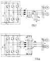
- FIGS. 3 and 4 show technically and economically feasible proposals for solving the problem.
- a first inductor L 1 and a second inductor L 2 is connected between each output terminal 3 of the converter 1 and the induction machine 4, the order of the two inductors not having an influence.
- the two inductors of which the first inductor L 1 is a so-called largely linear series choke and the second inductor L 2 is a current-compensated choke, is followed by a capacitance network CN with three strands, each of which consists of two capacitors C s connected in series.
- Each of the live lines between the inductors and the induction machine 4 is led to the center of one of the strands of the capacitance network.
- connection ends of the strands of the capacitance network CN are led to the positive or negative connection 5 or 6 of the DC voltage intermediate circuit 2.
- Each first inductor L 1 forms, together with the two capacitors C s of the line connected downstream, the LC low-pass filter required for generating the sinusoidal voltage between the live lines to the induction machine 4. As shown, this is connected to the DC link 2.
- a particular advantage of these current-compensated inductors or chokes is that, with a relatively small construction volume, high inductance values can be achieved, the size of the inductor naturally having to be designed for the asymmetrical currents that occur. Since these current-compensated chokes only generate negligible voltage drops for normal operating current, can be created by suitable dimensioning of a first inductance L 1 and the respective capacitors C s connected to this LC low-pass filter, which is effective for all the above-mentioned disadvantageous problems.
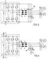
- FIG. 4 shows a further exemplary embodiment of a circuit for a technically and economically feasible solution to the problems mentioned.
- a first inductor (linear series choke) L 1 and a second inductor (current-compensated choke) L 2 which is followed by a capacitance network CN ' .
- a ⁇ connection of the capacitance network CN with connection of one or three capacitors to ground potential also results in an equivalent solution.
- capacitors C f can also be connected from the DC voltage intermediate circuit 2 to the ground potential in order to reduce radio interference suppression problems.
- asymmetrical currents can flow through the capacitors C s , C e and C f .
Abstract
Description
Die vorliegende Erfindung liegt auf dem Gebiet der Frequenzumrichter oder Wechselrichter, die seit einigen Jahren verstärkt zur Drehzahlregelung von Drehfeldmaschinen eingesetzt werden. Dabei werden vorwiegend sogenannte U-Wechselrichter mit einem Gleichspannungs-Zwischenkreis verwendet. Der letztere bildet aus der normalerweise konstanten Netzspannung eine Gleichspannung. Diese wird im Wechselrichter mittels Leistungshalbleiterschaltern geschaltet, wodurch das gewünschte dreiphasige Drehstromnetz mit veränderlicher Spannung und Frequenz bereitgestellt wird.The present invention is in the field of frequency converters or inverters, which have been increasingly used for speed control of induction machines for several years. So-called U inverters with a DC voltage intermediate circuit are predominantly used. The latter forms a DC voltage from the normally constant mains voltage. This is switched in the inverter by means of power semiconductor switches, whereby the desired three-phase three-phase network with variable voltage and frequency is provided.
Als Leistungshalbleiter werden beispielsweise FET's oder IGBT's (Feldeffekt- bzw. Insulated-Gate-Bipolar-Transistoren) verwendet, also Bauteile, die zur Erzielung eines möglichst hohen Wirkungsgrades sehr schnell und mit sehr steilen Spannungsanstiegszeiten der Impulse arbeiten. Diese an sich vorteilhafte Eigenschaft führt zu folgenden Problemen beim Betrieb dieser Umrichter:
- Unzulässig hohe Beanspruchung der Isolation angeschlossener Drehfeldmaschinen durch sehr steile Spannungsimpulse (du/dt-Belastung): Insbesondere bei kürzeren Anschlusskabeln zu den angeschlossenen Drehfeldmaschinen gelangen sehr steile Spannungsimpulse an deren Wicklungsisolation. Dies führt zu einer ständig sehr hohen Umpolarisation innerhalb der Isolation, die zu Ausfällen aufgrund von Ermüdungserscheinungen der Wicklungsisolation und somit zur Reduzierung der Lebensdauer von Drehfeldmaschinen führt.
- Unzulässig hohe Beanspruchung der Isolation angeschlossener Drehfeldmaschinen durch Überspannungen bei längeren Anschlusskabeln: Je nach Leitungslänge zwischen Umrichter und Drehfeldmaschinen können infolge von Signallaufzeiten und Reflexionen der Impulse Überpannungen auftreten, die mehr als das Doppelte der Zwischenkreisspannung betragen können. dies führt ebenfalls zu einer unzulässigen Belastung der Wicklungsisolation, die die Lebensdauer eines Antriebs erheblich reduzieren kann.
- Unzulässige Beeinflussung oder Funktionsbeeinträchtigung benachbarter Baugruppen oder von zum Verbindungskabel zwischen Umrichter und Drehmaschinen parallel geführten Kabeln: Bedingt durch die physikalische Arbeitsweise der Umrichter, d. h. durch die sehr kurzen Spannungs-Anstiegs- und -Abfallzeiten der Impulse, können über die kapazitive und induktive Kopplung sowie über Abstrahlung Beeinflussungen, insbesondere Fehlfuntktionen oder Ausfälle, benachbarter elektrischer Baugruppen oder Geräte auftreten. Die vom Umrichter erzeugten Spannungsimpulse wirken nicht nur zwischen den angeschlossenen Leitungsadern (symmetrische Spannungen), sondern es treten auch Spannungssprünge gegenüber dem Erdpotential auf (unsymmetrische oder asymmetrische Störspannungen). Dies führt zu parasitären Störströmen im Erdungssystem, welche bei einem schlecht ausgeführten Erdungssystem benachbarte Baugruppen oder Kabel störend beeinflussen können.
Häufig werden zur Erfüllung der Normen bezuglich Störfestigkeit und Funkentstörung zwischen Umrichter und Drehmaschinen geschirmte Verbindungskabel eingesetzt, durch welche die kapazitive Kopplung und damit die Beeinflussbarkeit benachbarter Kabel und Baugruppen reduziert werden soll. Dabei treten aber infolge der Koppelkapazität der geschirmten Verbindungskabel, das ist die Kapazität zwischen Einzeladern und Schirm, hochfrequente Ströme auf, welche im Kabelschirm fliessen und über magnetische Kopplung Störströme in benachbarten Kabeln induzieren, was zu Beeinflussungen führen kann. Ausserdem kann sich aufgrund der hochfrequenten Ströme und der Länge des Kabels ein Teil der vorhandenen Störenergie in Form von Abstrahlung vom Kabel lösen und benachbarte Baugruppen und Geräte unzulässig beeinflussen. Dieser Effekt tritt natürlich auch bei ungeschirmten Kabeln auf. - Unzulässige Beanspruchung der Leistungshalbleiter im Umrichter durch die ausgangsseitig angeschlossenen Leitungen zu den Drehfeldmaschinen: Bei längeren Verbindungskabeln zwischen Umrichter und Drehmaschinen werden die Leistungshalbleiter durch die Kabelkapazität zusätzlich mit Auf- und Entladeströmen belastet, welche der Umrichter zusätzlich zu den erforderlichen Betriebsströmen der Drehmaschinen liefern muss. Diese zusätzliche Belastung steigt umso mehr, je höher die Schaltfrequenz des Umrichters gewählt wird. Da heutige Umrichter zumeist kurzschlussfest sind oder zumindest über eine Stromregelung verfügen, muss für Anwendungen mit längeren Verbindungskabeln ein Umrichter gewählt werden, der diesen zusätzlichen symmetrischen Strom zwischen den Leitungen ungefährdet verarbeiten kann. Das bedeutet für den Anwender, dass er eventuell einen erheblich leistungsstärkeren und teureren Umrichter verwenden muss.
- Impermissibly high stress on the insulation of connected induction machines due to very steep voltage pulses (du / dt load): Especially with shorter connection cables to the connected induction machines, very steep voltage pulses reach their winding insulation. This leads to a constantly very high polarity reversal within the insulation, which leads to failures due to fatigue in the winding insulation and thus to a reduction in the service life of induction machines.
- Impermissibly high stress on the insulation of connected induction machines due to overvoltages with longer connection cables: Depending on the cable length between the converter and induction machines, signal run times and reflections can result Overvoltages occur which can be more than double the DC link voltage. this also leads to an impermissible load on the winding insulation, which can significantly reduce the service life of a drive.
- Impermissible influencing or functional impairment of neighboring assemblies or of cables routed parallel to the connecting cable between the converter and lathes: Due to the physical mode of operation of the converter, i.e. the very short voltage rise and fall times of the pulses, capacitive and inductive coupling as well as Radiation influences, in particular malfunctions or failures, of neighboring electrical assemblies or devices occur. The voltage pulses generated by the converter not only act between the connected line wires (symmetrical voltages), but there are also voltage jumps compared to the earth potential (asymmetrical or asymmetrical interference voltages). This leads to parasitic interference currents in the earthing system, which can interfere with neighboring assemblies or cables in a poorly designed earthing system.
Shielded connecting cables are often used to meet the standards regarding interference immunity and radio interference suppression between the converter and lathes, through which the capacitive coupling and thus the ability to influence neighboring cables and assemblies is to be reduced. However, due to the coupling capacity of the shielded connection cable, that is the capacitance between the single wires and the shield, high-frequency currents occur which flow in the cable shield and induce interference currents in neighboring cables via magnetic coupling, which can lead to interference. In addition, due to the high-frequency currents and the length of the cable, part of the existing interference energy in the form of radiation can detach from the cable and have an unacceptable influence on neighboring modules and devices. Of course, this effect also occurs with unshielded cables. - Impermissible stress on the power semiconductors in the converter due to the cables connected to the induction machines on the output side: In the case of longer connecting cables between the converter and lathes, the cable semiconductors additionally load the power semiconductors with charging and discharging currents, which the converter must supply in addition to the required operating currents of the lathes. This additional load increases the higher the switching frequency of the converter is selected. Since today's inverters are mostly short-circuit proof or at least have current control, an inverter must be selected for applications with longer connecting cables that can safely process this additional symmetrical current between the lines. For the user, this means that he may have to use a considerably more powerful and expensive converter.
Bei geschirmten Verbindungskabeln kommt es schon bei mittleren Kabellängen zu unzulässigen Belastungen der Leistungshalbleiter, indem durch die Koppelkapazität des Kabelschirms unsymmetrische Ströme auftreten, welche die Leistungshalbleiter zusätzlich belasten.In the case of shielded connection cables, even the medium cable lengths are subject to impermissible loads on the power semiconductors due to the fact that the coupling capacitance of the cable shield causes asymmetrical currents which put an additional load on the power semiconductors.
Die Erfindung betrifft nun eine Einrichtung zur Begrenzung der Änderungsgeschwindigkeit der ausgangsseitigen Spannung eines über einen Gleichspannungs-Zwischenkreis selbstgeführten Umrichters, welcher Ausgangslemmen für den Anschluss von mindestens einer Drehfeldmaschine sowie eine zwischen jeder Ausgangsklemme und der mindestens einen Drehfeldmaschine angeordnete Indüktivität aufweist.The invention now relates to a device for limiting the rate of change of the output-side voltage of a converter which is self-controlled via a DC voltage intermediate circuit and which has output terminals for the connection of at least one induction machine and an inductance arranged between each output terminal and the at least one induction machine.
Bei einer in der DE-A-41 35 680 beschriebenen Einrichtung dieser Art sind die Induktivitäten sogenannte Stromanstiegsbegrenzungsdrosseln, denen drei Diodenzweige mit je zwei Dioden nachgeschaltet sind. Die Stromanstiegsbegrenzungsdrosseln sind jeweils an das den Kathodenanschluss der einen Diode mit dem Anodenanschluss der anderen Diode eines Diodenzweigs verbindende Leitungsstück angeschlossen.In a device of this type described in DE-A-41 35 680, the inductors are so-called current rise limiting chokes, which are followed by three diode branches, each with two diodes. The current rise limiting chokes are each connected to the line piece connecting the cathode connection of one diode to the anode connection of the other diode of a diode branch.
Diese bekannte Einrichtung kann zwar einige der vorstehend aufgezählten Probleme, insbesondere die Beanspruchung der Isolation der angeschlossenen Drehfeldmaschinen durch steile Spannungsimpulse oder die Beanspruchung der Leistungshalbleiter durch die Verbindungskabel, merklich reduzieren, sie ist aber hinsichlich anderer Probleme praktisch unwirksam. Dies hängt damit zusammen, dass diese Einrichtung im wesentlichen nur auf die symmetrischen Spannungen, also auf die Spannungen zwischen den spannungsführenden Leitungen, wirkt und die unsymmetrischen Spannungen praktisch nicht beeinflusst.Although this known device can noticeably reduce some of the problems listed above, in particular the stress on the insulation of the connected induction machine due to steep voltage pulses or the stress on the power semiconductors due to the connecting cable, it is practically ineffective with regard to other problems. This is due to the fact that this device essentially only acts on the symmetrical voltages, that is to say on the voltages between the live lines, and practically does not influence the asymmetrical voltages.
Durch die Erfindung soll eine Einrichtung der genannten Art angegeben werden, die sowohl auf symmetrische als auch auf unsymmetrische Störspannungen wirkt und dadurch die eingangs genannten Probleme beseitigt oder zumindest ganz wesentlich reduziert.The invention is intended to provide a device of the type mentioned which acts both on symmetrical and on asymmetrical interference voltages and thereby eliminates or at least significantly reduces the problems mentioned at the outset.
Die erfindungsgemässe Lösung dieser Aufgabe ist dadurch gekennzeichnet, dass zwischen jeder Ausgangsklemme und der mindestens einen Drehfeldmaschine zwei Induktivitäten, und zwar eine weitestgehend lineare Längsdrossel und eine stromkompensierte Drossel geschaltet sind, dass den Drosseln ein Kapazitätsnetzwerk mit mehreren Strängen nachgeschaltet ist, und dass jede der spannungsführenden Leitungen zwischen den Drosseln und der mindestens einen Drehfeldmaschine an einen der Stränge des Kapazitätsnetzwerks geführt ist.The solution to this problem according to the invention is characterized in that two inductors, namely a largely linear series choke and a current-compensated choke, are connected between each output terminal and the at least one induction machine, that a capacitance network with several strings is connected downstream of the chokes, and that each of the live conductors Lines between the chokes and the at least one induction machine is routed to one of the strands of the capacitance network.
Die erfindungsgemässe Einrichtung reduziert die Anstiegs- und Abfallflanken der vom Umrichter erzeugten Spannungsimpulse,wodurch die Probleme mit der Beanspruchung der Isolation der Drehfeldmaschinen auf ein sinnvolles Mass reduziert werden. Gleichzeitig wirkt sie auf die unsymmetrischen Spannungen gegenüber dem Erdpotential, wodurch auch die durch diese unsymmetrischen Spannungen verursachten Störungen ausgeschaltet oder zumindest weitgehend reduziert werden.The device according to the invention reduces the rising and falling edges of the voltage pulses generated by the converter, as a result of which the problems with the stress on the insulation of the induction machines are reduced to a reasonable degree. At the same time, it affects the asymmetrical voltages with respect to the earth potential, whereby the disturbances caused by these asymmetrical voltages are also eliminated or at least largely reduced.
Im folgenden wird die Erfindung anhand von Ausführungsbeispielen und der Zeichnungen näher erläutert; dabei zeigt:
- Fig. 1
- eine Einrichtung zur Begrenzung der Änderungsgeschwindigkeit der Ausgangsspannung bei selbstgeführten Umrichtern nach dem Stand der Technik; und
- Fig. 2 - 4
- je ein Ausführungsbeispiel einer erfindungsgemässen Lösung einer Einrichtung der in Fig. 1 gezeigten Art.
- Fig. 1
- a device for limiting the rate of change of the output voltage in self-commutated converters according to the prior art; and
- Figs. 2-4
- one embodiment of a solution according to the invention of a device of the type shown in FIG. 1.
Fig. 1 zeigt einen zur Drehzählregelung von Drehfeldmaschinen vorgesehenen Wechselrichter oder Frequenzumrichter 1, der an einen durch einen Kondensator symbolisierten Gleichspannungs-Zwischenkreis 2 angeschlossen ist. Dieser ist durch einen an das Versorgungsnetz mit üblicherweise konstanter Spannung und konstanter Frequenz angeschlossenen Netzgleichrichter (nicht dargestellt) gespeist. Der Umrichter 1 schaltet die Gleichspannung des Gleichspannungs-Zwischenkreises 2 mittels Leistungshalbleiterschaltern und stellt an seinen Ausgangsklemmen 3 für die angeschlossenen Drehfeldmaschinen 4 (z.B. Motoren M) das gewünschte dreiphasige Drehstromnetz mit veränderlicher Frequenz und Spannung bereit. Wenn in dieser Beschreibung von Drehfeldmaschinen oder von Drehfeldmaschine die Rede ist, dann ist immer beides, sowohl eine einzelne Maschine als auch eine Maschinengruppe, gemeint.1 shows an inverter or
Als Leistungshalbleiterschalter werden beispielsweise FET's oder IGBT's verwendet, die sehr schnell und mit sehr steilen Anstiegsflanken der Impulse arbeiten. Dadurch werden zwar die Verluste im Umrichter 1 möglichst gering gehalten, so dass mit einem sehr hohen Wirkungsgrad gearbeitet werden kann, es ergeben sich aber die vorne in der Beschreibungseinleitung aufgezählten nachteiligen Probleme. Ein Teil davon, und zwar die auf die Spannungen zwischen den spannungsführenden Leitern zurückzuführenden Probleme, lässt sich durch das Einfügen von Induktivitäten L und Kapazitäten C in Form eines LC-Tiefpasses in die Leitung zwischen Umrichter 1 und Drehfeldmaschinen 4 eliminieren. Die dargestellte Schaltung wirkt jedoch fast ausschliesslich auf die symmetrischen Spannungen Usy zwischen den spannungsführenden Leitungen.FETs or IGBTs are used as power semiconductor switches, for example, which work very quickly and with very steep rising edges of the pulses. Although the losses in the
Hingegen bleiben bei der in Fig. 1 dargestellten Schaltung die durch Potentialsprünge am Ausgang des Umrichters 1 erzeugten unsymmetrischen Spannungen Uus gegenüber dem Erdpotential weitestgehend erhalten. Man könnte zwar theoretisch mit relativ hohen Induktivitätswerten die Spannungsanstiegszeiten wesentlich verlängern, was aber die Verwendung voluminöser und teurer Induktivitäten erfordern würde. Ausserdem würde durch den Einsatz grosser Induktivitäten an diesen ein relativ grosser Spannungsabfall hervorgerufen, der seinerseits die für die Drehfeldmaschine zur Verfügung stehende Spannung reduzieren wurde. Damit würde aber die Drehfeldmaschine nicht mehr ihre volle Antriebsleistung erhalten, wodurch das ganze aus Umrichter 1 und Drehfeldmaschine 4 bestehende System in Frage gestellt wäre.In contrast, in the circuit shown in FIG. 1, the asymmetrical voltages U us generated by potential jumps at the output of the
Fig. 2 zeigt eine theoretisch mögliche Variante, die auch die unsymmetrischen Spannungen weitgehend reduziert und somit alle vorne diskutierten nachteiligen Eigenschaften der bekannten Umrichter weitgehend beseitigen oder reduzieren könnte. Bei dieser Variante sind an jede Induktivität L zwei im Stern geschaltete Kapazitäten C angeschlossen, und die Sternpunkte sind jeweils mit einem Pol der Zwischenkreisspannung des Umrichters 1 verbunden. Mit dieser Schaltung können sowohl sinusförmige, symmetrische Spannungen erzeugt, als auch die unsymmetrischen Spannungen in ihrer Anstiegs- und Abfallzeit nach unten begrenzt werden. Allerdings müssen die unsymmetrischen Ströme Ius in der Rückführung zum Gleichspannungs-Zwischenkreis 2 gering gehalten werden, um nicht die Leistungshalbleiter zusätzlich zu belasten. Auch hier wurden wieder relativ hohe Induktivitätswerte benötigt, die zu den schon im Zusammenhang mit Fig. 1 diskutierten Problemen führen würden.FIG. 2 shows a theoretically possible variant that also largely reduces the asymmetrical voltages and thus could largely eliminate or reduce all the disadvantageous properties of the known converters discussed above. In this variant, two capacitances C connected in a star are connected to each inductance L, and the star points are each connected to one pole of the intermediate circuit voltage of the
Die in Figur 2 dargestellte Einrichtung vermeidet zwar alle aufgezählten Nachteile, die praktische Realisierung dieses Ausführungsbeispiels kann aber an wirtschaftlichen und technischen Schwierigkeiten scheitern. Die Figuren 3 und 4 zeigen dagegen technisch und wirtschaftlich machbare Vorschläge zur Lösung der gestellten Aufgabe.The device shown in FIG. 2 avoids all of the disadvantages listed, but the practical implementation of this exemplary embodiment can fail due to economic and technical difficulties. FIGS. 3 and 4, on the other hand, show technically and economically feasible proposals for solving the problem.
Bei der in Fig. 3 dargestellten Schaltung ist zwischen jeder Ausgangsklemme 3 des Umrichters 1 und der Drehfeldmaschine 4 eine erste Induktivität L₁ und eine zweite Induktivität L₂ geschaltet, wobei die Reihenfolge der beiden Induktivitäten nicht von Einfluss ist. Den beiden Induktivitäten, von denen die erste Induktivität L₁ eine sogenannte weitestgehend lineare Längsdrossel und die zweite Induktivität L₂ eine stromkompensierte Drossel ist, ist ein Kapazitätsnetzwerk CN mit drei Strängen nachgeschaltet, von denen jeder aus zwei in Reihe geschalteten Kondensatoren Cs besteht. Jede der spannungsführenden Leitungen zwischen den Induktivitäten und der Drehfeldmaschine 4 ist an den Mittelpunkt eines der Stränge des Kapazitätsnetzwerks geführt. Die Anschlussenden der Stränge des Kapazitätsnetzwerks CN sind auf den Plus- oder den Minusanschluss 5 bzw. 6 des Gleichspannungs-Zwischerikreises 2 geführt. Jede erste Induktivität L₁ bildet zusammen mit den beiden Kondensatoren Cs des ihr nachgeschalteten Stranges den für die Erzeugung der sinusförmigen Spannung zwischen den spannungsführenden Leitungen zur Drehfeldmaschine 4 erforderlichen LC-Tiefpass. Dieser ist darstellungsgemäss an den Gleichspannungs-Zwischenkreis 2 angebunden.In the circuit shown in Fig. 3, a
Stromkompensierte Drosseln sind so ausgebildet, dass sich bei normalem Betriebsstrom (Motorstrom) die im Kern erzeugten magnetischen Flüsse aufheben und die Induktivitäten praktisch wirkungslos sind. Fliessen jedoch unsymmetrische Ströme gegenüber Erdpotential ab oder an den Gleichspannungs-Zwischenkreis 2 zurück so ist die Summe der gesamten Ströme ungleich, und die magnetischen Flüsse heben sich nicht mehr auf.Current-compensated chokes are designed in such a way that the magnetic fluxes generated in the core cancel each other out at normal operating current (motor current) and the inductances are practically ineffective. However, if asymmetrical currents flow from earth potential or back to the
Ein besonderer Vorteil dieser stromkompensierten Induktivitäten oder Drosseln liegt darin, dass bei relativ kleinem Bauvolumen hohe Induktivitätswerte erreicht werden können, wobei selbstverständlich die Grösse der Induktivität auf die auftretenden unsymmetrischen Ströme ausgelegt sein muss. Da diese stromkompensierten Drosseln für den normalen Betriebsstrom nur vernachlässigbar geringe Spannungsabfälle erzeugen, kann durch geeignete Dimensionierung des aus einer ersten Induktivität L₁ und den jeweiligen mit dieser verbundenen Kondensatoren Cs gebildeten LC-Tiefpasses eine für alle aufgezählten nachteiligen Probleme wirksame kompakte Einrichtung erstellt werden.A particular advantage of these current-compensated inductors or chokes is that, with a relatively small construction volume, high inductance values can be achieved, the size of the inductor naturally having to be designed for the asymmetrical currents that occur. Since these current-compensated chokes only generate negligible voltage drops for normal operating current, can be created by suitable dimensioning of a
Ein weiterer Vorteil der in Fig. 3 dargestellten Schaltung besteht darin, dass bei dieser wegen der Reduzierung der un- oder asymmetrischen Störspannungen auf die sonst erforderlichen teuren geschirmten Verbindungskabel zwischen Umrichter und Motor verzichtet werden kann, woraus sich eine nicht unerhebliche Reduktion der Installationskosten ergibt.Another advantage of the circuit shown in Fig. 3 is that it can be dispensed with because of the reduction of the non- or asymmetrical interference voltages on the otherwise expensive shielded connection cables between the converter and motor, which results in a not inconsiderable reduction in installation costs.
In Fig. 4 ist ein weiteres Ausführungsbeispiel einer Schaltung für eine technisch und wirtschaftlich machbare Lösung der genannten Probleme dargestellt. Auch bei dieser Schaltung ist so wie bei der von Fig. 3 zwischen jeder Ausgangsklemme 3 des Umrichters 1 und der Drehfeldmaschine 4 eine erste Induktivität (lineare Längsdrossel) L₁ und eine zweite Induktivität (stromkompensierte Drossel) L₂ geschaltet, denen ein Kapazitätsnetzwerk CN' nachgeschaltet ist. Dieses unterscheidet sich von dem in Fig. 3 dargestellten Kapazitätsnetzwerk CN dadurch, dass seine drei Stränge nur je einen Kondensator Cs enthalten und zu einem Sternpunkt zusammengeführt sind. Dieser ist zur Ableitung der unsymmetrischen Ströme über eine weitere Kapazität Ce zum Erdpotential geschaltet. Auch eine Δ-Schaltung des Kapazitätsnetzwerks CN mit Anschaltung von einem oder drei Kondensatoren zum Erdpotential ergibt eine gleichwertige Lösung.4 shows a further exemplary embodiment of a circuit for a technically and economically feasible solution to the problems mentioned. In this circuit as well as in Fig. 3 between each
Darstellungsgemäss können zur Verringerung von Funk-Entstörproblemen auch vom Gleichspannungs-Zwischenkreis 2 zum Erdpotential Kondensatoren Cf geschaltet sein. In diesem Fall können also unsymmetrische Stöme über die Kondensatoren Cs, Ce und Cf fliessen.According to the illustration, capacitors C f can also be connected from the DC voltage
Claims (7)
Applications Claiming Priority (2)
| Application Number | Priority Date | Filing Date | Title |
|---|---|---|---|
| CH1462/94 | 1994-05-11 | ||
| CH01462/94A CH693523A5 (en) | 1994-05-11 | 1994-05-11 | Means for limiting the Aenderungsgeschwindigkeit the output-side voltage of a self-commutated multiphase converter. |
Publications (2)
| Publication Number | Publication Date |
|---|---|
| EP0682401A1 true EP0682401A1 (en) | 1995-11-15 |
| EP0682401B1 EP0682401B1 (en) | 1998-05-27 |
Family
ID=4211045
Family Applications (1)
| Application Number | Title | Priority Date | Filing Date |
|---|---|---|---|
| EP95106488A Revoked EP0682401B1 (en) | 1994-05-11 | 1995-04-28 | Limiting device for the output voltage slope of a self-commutated converter |
Country Status (4)
| Country | Link |
|---|---|
| EP (1) | EP0682401B1 (en) |
| AT (1) | ATE166753T1 (en) |
| CH (1) | CH693523A5 (en) |
| DE (1) | DE59502313D1 (en) |
Cited By (7)
| Publication number | Priority date | Publication date | Assignee | Title |
|---|---|---|---|---|
| DE19637290A1 (en) * | 1996-09-13 | 1998-03-19 | Asea Brown Boveri | Converter circuit arrangement with load-side filter |
| DE19736786A1 (en) * | 1997-08-23 | 1999-02-25 | Asea Brown Boveri | U-converter |
| DE19814059A1 (en) * | 1998-03-30 | 1999-10-07 | Asea Brown Boveri | Load-side filter arrangement for a converter circuit arrangement |
| WO2002084851A1 (en) * | 2001-04-11 | 2002-10-24 | Abb Ab | Vsc-converter |
| EP1296441A1 (en) * | 2001-09-25 | 2003-03-26 | ABB Schweiz AG | Power generating arrangement |
| DE102004004627A1 (en) * | 2004-01-29 | 2005-08-18 | Siemens Ag | AC motor voltage supply is provided by circuit that reduces symmetrical and asymmetrical voltage components |
| EP2367272A3 (en) * | 2010-02-25 | 2017-06-21 | Kostal Industrie Elektrik GmbH | Inverter |
Families Citing this family (6)
| Publication number | Priority date | Publication date | Assignee | Title |
|---|---|---|---|---|
| DE102005045554B3 (en) * | 2005-09-23 | 2007-04-26 | Siemens Ag | Filter e.g. for filtering interfering currents, has grounded housing having capacitor circuit and device for electrical contacting of capacitor circuit with device actuated with two contact areas and contacting element |
| DE102008026869B4 (en) | 2008-06-05 | 2014-11-20 | Siemens Aktiengesellschaft | Lossy three-phase low-pass filter |
| DE102008031296A1 (en) | 2008-07-02 | 2009-08-20 | Siemens Aktiengesellschaft | Inductor device for e.g. output-sinusoidal filter of frequency converter, has three coils arranged on core from magnetic material, and another core arranged above three coils and forming single inductor acting as longitudinal inductance |
| DE102009031547B3 (en) * | 2009-07-02 | 2010-10-21 | Siemens Aktiengesellschaft | Method for controlling load-side converter of intermediate voltage circuit inverter, involves connecting output terminals, electric motor and low pass filter with push-pull choke, capacitor per output phase and common mode choke |
| DE102010047338B4 (en) | 2010-10-01 | 2016-07-21 | Audi Ag | Motor vehicle with circuit arrangement and method for operating such a motor vehicle |
| DE102010047994A1 (en) | 2010-10-08 | 2012-04-12 | Audi Ag | Circuit arrangement for motor vehicle, has induction machine whose phase outputs are connected to inverters at output voltage terminals side, where current flows through winding wires in specific direction |
Citations (8)
| Publication number | Priority date | Publication date | Assignee | Title |
|---|---|---|---|---|
| DE3318480A1 (en) * | 1983-05-18 | 1984-11-22 | Licentia Gmbh | Thyristor-controlled rectifier having a good dynamic response during partial load |
| JPS60106370A (en) * | 1983-11-15 | 1985-06-11 | Fuji Electric Co Ltd | Vvvf inverter |
| JPS62171462A (en) * | 1986-01-23 | 1987-07-28 | Fuji Electric Co Ltd | 3-phase noise filter for stationary power converter |
| JPS6474070A (en) * | 1987-09-11 | 1989-03-20 | Mitsubishi Electric Corp | Leak current reducing circuit |
| JPH0236795A (en) * | 1988-07-22 | 1990-02-06 | Mitsubishi Electric Corp | Device for prevention of electric leakage of inverter |
| DE4135680A1 (en) * | 1991-10-30 | 1993-05-06 | Andreas Prof. Dr.-Ing.Habil. 7000 Stuttgart De Boehringer | Inverter motor drive limiting rate of change of output currents - using inductive stages coupled between inverter outputs and motor units |
| DE9307806U1 (en) * | 1993-05-24 | 1993-08-26 | Siemens Ag | Inverter output filter |
| JPH0686563A (en) * | 1992-09-01 | 1994-03-25 | Mitsubishi Electric Corp | Power conversion apparatus |
-
1994
- 1994-05-11 CH CH01462/94A patent/CH693523A5/en not_active IP Right Cessation
-
1995
- 1995-04-28 DE DE59502313T patent/DE59502313D1/en not_active Revoked
- 1995-04-28 EP EP95106488A patent/EP0682401B1/en not_active Revoked
- 1995-04-28 AT AT95106488T patent/ATE166753T1/en not_active IP Right Cessation
Patent Citations (8)
| Publication number | Priority date | Publication date | Assignee | Title |
|---|---|---|---|---|
| DE3318480A1 (en) * | 1983-05-18 | 1984-11-22 | Licentia Gmbh | Thyristor-controlled rectifier having a good dynamic response during partial load |
| JPS60106370A (en) * | 1983-11-15 | 1985-06-11 | Fuji Electric Co Ltd | Vvvf inverter |
| JPS62171462A (en) * | 1986-01-23 | 1987-07-28 | Fuji Electric Co Ltd | 3-phase noise filter for stationary power converter |
| JPS6474070A (en) * | 1987-09-11 | 1989-03-20 | Mitsubishi Electric Corp | Leak current reducing circuit |
| JPH0236795A (en) * | 1988-07-22 | 1990-02-06 | Mitsubishi Electric Corp | Device for prevention of electric leakage of inverter |
| DE4135680A1 (en) * | 1991-10-30 | 1993-05-06 | Andreas Prof. Dr.-Ing.Habil. 7000 Stuttgart De Boehringer | Inverter motor drive limiting rate of change of output currents - using inductive stages coupled between inverter outputs and motor units |
| JPH0686563A (en) * | 1992-09-01 | 1994-03-25 | Mitsubishi Electric Corp | Power conversion apparatus |
| DE9307806U1 (en) * | 1993-05-24 | 1993-08-26 | Siemens Ag | Inverter output filter |
Non-Patent Citations (5)
| Title |
|---|
| PATENT ABSTRACTS OF JAPAN vol. 12, no. 13 (E - 573) 14 January 1988 (1988-01-14) * |
| PATENT ABSTRACTS OF JAPAN vol. 13, no. 295 (E - 783) 7 July 1989 (1989-07-07) * |
| PATENT ABSTRACTS OF JAPAN vol. 14, no. 190 (E - 918) 18 April 1990 (1990-04-18) * |
| PATENT ABSTRACTS OF JAPAN vol. 18, no. 345 (E - 1571) 29 June 1994 (1994-06-29) * |
| PATENT ABSTRACTS OF JAPAN vol. 9, no. 258 (E - 350) 16 October 1985 (1985-10-16) * |
Cited By (10)
| Publication number | Priority date | Publication date | Assignee | Title |
|---|---|---|---|---|
| DE19637290A1 (en) * | 1996-09-13 | 1998-03-19 | Asea Brown Boveri | Converter circuit arrangement with load-side filter |
| DE19736786A1 (en) * | 1997-08-23 | 1999-02-25 | Asea Brown Boveri | U-converter |
| US5999423A (en) * | 1997-08-23 | 1999-12-07 | Asea Brown Boveri Ag | Voltage converter with filter arrangement |
| DE19814059A1 (en) * | 1998-03-30 | 1999-10-07 | Asea Brown Boveri | Load-side filter arrangement for a converter circuit arrangement |
| US6160442A (en) * | 1998-03-30 | 2000-12-12 | Asea Brown Boveri Ag | Load-side filter arrangement for a converter circuit arrangement |
| WO2002084851A1 (en) * | 2001-04-11 | 2002-10-24 | Abb Ab | Vsc-converter |
| EP1296441A1 (en) * | 2001-09-25 | 2003-03-26 | ABB Schweiz AG | Power generating arrangement |
| US6774608B2 (en) | 2001-09-25 | 2004-08-10 | Abb Schweiz Ag | Turbine driven power generating device having DC voltage intermediate circuit and star connected filter capacitors |
| DE102004004627A1 (en) * | 2004-01-29 | 2005-08-18 | Siemens Ag | AC motor voltage supply is provided by circuit that reduces symmetrical and asymmetrical voltage components |
| EP2367272A3 (en) * | 2010-02-25 | 2017-06-21 | Kostal Industrie Elektrik GmbH | Inverter |
Also Published As
| Publication number | Publication date |
|---|---|
| ATE166753T1 (en) | 1998-06-15 |
| CH693523A5 (en) | 2003-09-15 |
| EP0682401B1 (en) | 1998-05-27 |
| DE59502313D1 (en) | 1998-07-02 |
Similar Documents
| Publication | Publication Date | Title |
|---|---|---|
| DE102008014898B4 (en) | Method for controlling a multiphase power converter with distributed energy stores at low output frequencies | |
| EP1040555B1 (en) | Converter connection assembly with a direct voltage intermediate circuit | |
| DE10143279B4 (en) | frequency converter | |
| DE112011101193B4 (en) | Leakage current reduction device | |
| WO2003090331A2 (en) | Power supply with a direct converter | |
| EP0682402B1 (en) | Output magnitudes rise limiting device for self-commutated constant voltage intermediate circuit converter | |
| EP0682401B1 (en) | Limiting device for the output voltage slope of a self-commutated converter | |
| EP1069673B1 (en) | Line filter | |
| EP1220431A1 (en) | Damping resonance peaks in an electric motor operated by an inverter with intermediate dc voltage link | |
| EP1211788A1 (en) | Damping resonance peaks in an electric motor operated by an inverter with intermediate dc voltage link | |
| EP0682395B1 (en) | Device for limiting the rate of change of currents and voltages between conductors or to earth and use thereof | |
| EP3513475B1 (en) | Installation for transmitting electrical power comprising a filter unit | |
| WO2017016692A1 (en) | Apparatus for avoiding harmful bearing currents | |
| EP0743744A2 (en) | Current converter | |
| DE10215236C1 (en) | Device for the inductive transmission of electrical energy | |
| WO2018113926A1 (en) | Power converter | |
| DE102009026479B4 (en) | Power semiconductor module with reduced oscillation tendency | |
| DE102015003225A1 (en) | inverter | |
| DE4430078A1 (en) | Circuit arrangement for avoiding switching losses in a pair of branches of a self-commutated converter having an impressed DC intermediate circuit (link) voltage | |
| DE19853693A1 (en) | Equipment for preventing surge voltages on the output wires of a self-commutated DC voltage changer uses a 3-phase DC voltage changer with 3-phase load and a circuit layout based on a lossy diode DC restorer forming a reference voltage. | |
| EP0819563A2 (en) | Power converter circuit | |
| DE19952886A1 (en) | Multi-way current regulator e.g. for electric motor, has local earth provided for each current regulator unit coupled to common line earth via earthing impedance | |
| DE102020000128A1 (en) | Drive system, comprising a first association and a second association | |
| EP3944483A1 (en) | Circuit arrangement with active rectifier circuit and its use in a synchronous machine | |
| EP2713499A1 (en) | Energy feed device with symmetrical connection of a direct current source to a grounded star point of a three-phase current network |
Legal Events
| Date | Code | Title | Description |
|---|---|---|---|
| PUAI | Public reference made under article 153(3) epc to a published international application that has entered the european phase |
Free format text: ORIGINAL CODE: 0009012 |
|
| AK | Designated contracting states |
Kind code of ref document: A1 Designated state(s): AT BE DE DK FR GB IE IT NL |
|
| 17P | Request for examination filed |
Effective date: 19960322 |
|
| 17Q | First examination report despatched |
Effective date: 19970415 |
|
| GRAG | Despatch of communication of intention to grant |
Free format text: ORIGINAL CODE: EPIDOS AGRA |
|
| GRAG | Despatch of communication of intention to grant |
Free format text: ORIGINAL CODE: EPIDOS AGRA |
|
| GRAH | Despatch of communication of intention to grant a patent |
Free format text: ORIGINAL CODE: EPIDOS IGRA |
|
| GRAH | Despatch of communication of intention to grant a patent |
Free format text: ORIGINAL CODE: EPIDOS IGRA |
|
| GRAA | (expected) grant |
Free format text: ORIGINAL CODE: 0009210 |
|
| TPAD | Observations filed by third parties |
Free format text: ORIGINAL CODE: EPIDOS TIPA |
|
| AK | Designated contracting states |
Kind code of ref document: B1 Designated state(s): AT BE DE DK FR GB IE IT NL |
|
| PG25 | Lapsed in a contracting state [announced via postgrant information from national office to epo] |
Ref country code: NL Free format text: LAPSE BECAUSE OF FAILURE TO SUBMIT A TRANSLATION OF THE DESCRIPTION OR TO PAY THE FEE WITHIN THE PRESCRIBED TIME-LIMIT Effective date: 19980527 Ref country code: IT Free format text: LAPSE BECAUSE OF FAILURE TO SUBMIT A TRANSLATION OF THE DESCRIPTION OR TO PAY THE FEE WITHIN THE PRESCRIBED TIME-LIMIT;WARNING: LAPSES OF ITALIAN PATENTS WITH EFFECTIVE DATE BEFORE 2007 MAY HAVE OCCURRED AT ANY TIME BEFORE 2007. THE CORRECT EFFECTIVE DATE MAY BE DIFFERENT FROM THE ONE RECORDED. Effective date: 19980527 |
|
| REF | Corresponds to: |
Ref document number: 166753 Country of ref document: AT Date of ref document: 19980615 Kind code of ref document: T |
|
| REF | Corresponds to: |
Ref document number: 59502313 Country of ref document: DE Date of ref document: 19980702 |
|
| GBT | Gb: translation of ep patent filed (gb section 77(6)(a)/1977) |
Effective date: 19980611 |
|
| ET | Fr: translation filed | ||
| REG | Reference to a national code |
Ref country code: IE Ref legal event code: FG4D Free format text: GERMAN |
|
| PG25 | Lapsed in a contracting state [announced via postgrant information from national office to epo] |
Ref country code: DK Free format text: LAPSE BECAUSE OF FAILURE TO SUBMIT A TRANSLATION OF THE DESCRIPTION OR TO PAY THE FEE WITHIN THE PRESCRIBED TIME-LIMIT Effective date: 19980827 |
|
| NLV1 | Nl: lapsed or annulled due to failure to fulfill the requirements of art. 29p and 29m of the patents act | ||
| PLBQ | Unpublished change to opponent data |
Free format text: ORIGINAL CODE: EPIDOS OPPO |
|
| PLBI | Opposition filed |
Free format text: ORIGINAL CODE: 0009260 |
|
| 26 | Opposition filed |
Opponent name: SIEMENS AKTIENGESELLSCHAFT, BERLIN UND MUENCHEN Effective date: 19990208 |
|
| PLBF | Reply of patent proprietor to notice(s) of opposition |
Free format text: ORIGINAL CODE: EPIDOS OBSO |
|
| PLAB | Opposition data, opponent's data or that of the opponent's representative modified |
Free format text: ORIGINAL CODE: 0009299OPPO |
|
| RAP2 | Party data changed (patent owner data changed or rights of a patent transferred) |
Owner name: SCHAFFNER EMV AG |
|
| R26 | Opposition filed (corrected) |
Opponent name: SIEMENS AG Effective date: 19990208 |
|
| PLBF | Reply of patent proprietor to notice(s) of opposition |
Free format text: ORIGINAL CODE: EPIDOS OBSO |
|
| REG | Reference to a national code |
Ref country code: GB Ref legal event code: IF02 |
|
| PLCK | Communication despatched that opposition was rejected |
Free format text: ORIGINAL CODE: EPIDOSNREJ1 |
|
| APBP | Date of receipt of notice of appeal recorded |
Free format text: ORIGINAL CODE: EPIDOSNNOA2O |
|
| APBQ | Date of receipt of statement of grounds of appeal recorded |
Free format text: ORIGINAL CODE: EPIDOSNNOA3O |
|
| APAH | Appeal reference modified |
Free format text: ORIGINAL CODE: EPIDOSCREFNO |
|
| PGFP | Annual fee paid to national office [announced via postgrant information from national office to epo] |
Ref country code: FR Payment date: 20060411 Year of fee payment: 12 |
|
| PGFP | Annual fee paid to national office [announced via postgrant information from national office to epo] |
Ref country code: AT Payment date: 20060418 Year of fee payment: 12 |
|
| PGFP | Annual fee paid to national office [announced via postgrant information from national office to epo] |
Ref country code: DE Payment date: 20060419 Year of fee payment: 12 |
|
| PGFP | Annual fee paid to national office [announced via postgrant information from national office to epo] |
Ref country code: GB Payment date: 20060420 Year of fee payment: 12 |
|
| PGFP | Annual fee paid to national office [announced via postgrant information from national office to epo] |
Ref country code: IE Payment date: 20060427 Year of fee payment: 12 |
|
| PGFP | Annual fee paid to national office [announced via postgrant information from national office to epo] |
Ref country code: BE Payment date: 20060502 Year of fee payment: 12 |
|
| APBU | Appeal procedure closed |
Free format text: ORIGINAL CODE: EPIDOSNNOA9O |
|
| RDAF | Communication despatched that patent is revoked |
Free format text: ORIGINAL CODE: EPIDOSNREV1 |
|
| RDAG | Patent revoked |
Free format text: ORIGINAL CODE: 0009271 |
|
| STAA | Information on the status of an ep patent application or granted ep patent |
Free format text: STATUS: PATENT REVOKED |
|
| 27W | Patent revoked |
Effective date: 20070123 |
|
| PLAB | Opposition data, opponent's data or that of the opponent's representative modified |
Free format text: ORIGINAL CODE: 0009299OPPO |