EP0580341A2 - Integrated circuit and cordless telephone using the integrated circuit - Google Patents
Integrated circuit and cordless telephone using the integrated circuit Download PDFInfo
- Publication number
- EP0580341A2 EP0580341A2 EP93305466A EP93305466A EP0580341A2 EP 0580341 A2 EP0580341 A2 EP 0580341A2 EP 93305466 A EP93305466 A EP 93305466A EP 93305466 A EP93305466 A EP 93305466A EP 0580341 A2 EP0580341 A2 EP 0580341A2
- Authority
- EP
- European Patent Office
- Prior art keywords
- microcontroller
- interrupt
- external
- port
- keypad
- Prior art date
- Legal status (The legal status is an assumption and is not a legal conclusion. Google has not performed a legal analysis and makes no representation as to the accuracy of the status listed.)
- Withdrawn
Links
Images


Classifications
-
- H—ELECTRICITY
- H04—ELECTRIC COMMUNICATION TECHNIQUE
- H04M—TELEPHONIC COMMUNICATION
- H04M1/00—Substation equipment, e.g. for use by subscribers
- H04M1/72—Mobile telephones; Cordless telephones, i.e. devices for establishing wireless links to base stations without route selection
- H04M1/725—Cordless telephones
-
- H—ELECTRICITY
- H04—ELECTRIC COMMUNICATION TECHNIQUE
- H04B—TRANSMISSION
- H04B1/00—Details of transmission systems, not covered by a single one of groups H04B3/00 - H04B13/00; Details of transmission systems not characterised by the medium used for transmission
- H04B1/38—Transceivers, i.e. devices in which transmitter and receiver form a structural unit and in which at least one part is used for functions of transmitting and receiving
- H04B1/40—Circuits
-
- H—ELECTRICITY
- H04—ELECTRIC COMMUNICATION TECHNIQUE
- H04M—TELEPHONIC COMMUNICATION
- H04M1/00—Substation equipment, e.g. for use by subscribers
- H04M1/72—Mobile telephones; Cordless telephones, i.e. devices for establishing wireless links to base stations without route selection
- H04M1/725—Cordless telephones
- H04M1/73—Battery saving arrangements
-
- G—PHYSICS
- G06—COMPUTING; CALCULATING OR COUNTING
- G06F—ELECTRIC DIGITAL DATA PROCESSING
- G06F11/00—Error detection; Error correction; Monitoring
- G06F11/07—Responding to the occurrence of a fault, e.g. fault tolerance
- G06F11/0703—Error or fault processing not based on redundancy, i.e. by taking additional measures to deal with the error or fault not making use of redundancy in operation, in hardware, or in data representation
- G06F11/0751—Error or fault detection not based on redundancy
- G06F11/0754—Error or fault detection not based on redundancy by exceeding limits
- G06F11/0757—Error or fault detection not based on redundancy by exceeding limits by exceeding a time limit, i.e. time-out, e.g. watchdogs
-
- G—PHYSICS
- G06—COMPUTING; CALCULATING OR COUNTING
- G06F—ELECTRIC DIGITAL DATA PROCESSING
- G06F11/00—Error detection; Error correction; Monitoring
- G06F11/22—Detection or location of defective computer hardware by testing during standby operation or during idle time, e.g. start-up testing
- G06F11/26—Functional testing
- G06F11/261—Functional testing by simulating additional hardware, e.g. fault simulation
-
- Y—GENERAL TAGGING OF NEW TECHNOLOGICAL DEVELOPMENTS; GENERAL TAGGING OF CROSS-SECTIONAL TECHNOLOGIES SPANNING OVER SEVERAL SECTIONS OF THE IPC; TECHNICAL SUBJECTS COVERED BY FORMER USPC CROSS-REFERENCE ART COLLECTIONS [XRACs] AND DIGESTS
- Y02—TECHNOLOGIES OR APPLICATIONS FOR MITIGATION OR ADAPTATION AGAINST CLIMATE CHANGE
- Y02D—CLIMATE CHANGE MITIGATION TECHNOLOGIES IN INFORMATION AND COMMUNICATION TECHNOLOGIES [ICT], I.E. INFORMATION AND COMMUNICATION TECHNOLOGIES AIMING AT THE REDUCTION OF THEIR OWN ENERGY USE
- Y02D30/00—Reducing energy consumption in communication networks
- Y02D30/70—Reducing energy consumption in communication networks in wireless communication networks
Definitions
- the present invention relates to integrated circuits (IC's), such as IC's involved with the speech, control channel, or microcontroller portions of a modem, or with the man-machine interface functions of a cordless telephone.
- IC's integrated circuits
- the standard telephone consists of a base unit and a handset unit connected to each other by an electrical cord.
- the base unit itself is connected by another cord to a receptacle on a wall, telephone pole or a similar immovable structure to which the telephone network line extends. Because of this connection to an immovable structure, the range of movement of the operator of the telephone is quite limited. Even when the cords connecting the handset unit to the base unit and the based unit to the wall are long, it can be cumbersome either to move the entire telephone around to make calls from difference locations or to walk around with the handset unit once a call has been placed. The simple fact that there is always a continuous physical connection between the person making the phone call and the immovable wall or other fixed structure can be a great inconvenience.
- the cordless telephone represents a significant improvement over the standard telephone.
- the base unit is still connected to the receptacle on the immovable wall or the like by a cord so that message signals from the telephone network line may be received and transmitted.
- the handset unit of the cordless telephone is an independently operative unit from which calls may be made and by which calls may be received with no physical connection to the base unit.
- the handset unit has a transmitting/receiving system or transceiver, a loudspeaker in an earpiece and a microphone in a mouthpiece.
- the base unit and the handset unit of the cordless telephone communicate with each other over a communication channel established by the transmission and reception of electromagnetic waves, conventionally radio waves.
- the handset unit may then be taken considerable distances from the base unit while still making and receiving telephone calls. Since there is no telephone cord extending between the handset unit and the base unit, the operator is free to move about without hindrance.
- U.S. Patent 5,005,150 to Dent et al. discloses a digital signal processor incorporated in an integrated circuit to convert pulse code modulated (PCM) signals to adaptive differential pulse code modulation (ADPCM) signals in cordless telephones.
- PCM pulse code modulated
- ADPCM adaptive differential pulse code modulation
- cordless telephone IC development has been hampered because of power consumption considerations.
- Cordless telephones have to be battery-powered if they are to be mobile and heretofore conventional microprocessors or microcomputers have been considered to consume too much energy to be used, in a practical manner, in mass-produced cordless telephones. Additionally, conventional microprocessors or microcomputers have been considered to be too expensive for such applications.
- IC' s for cordless telephones
- aspects of such phones that can be improved by intelligent use of IC' s.
- Examples of these aspects include having an IC that supports an in-circuit emulation mode, having a keypad reporting mechanism with reduced software overhead and simplified hardware, having advanced noise suppression mechanisms, having a low power emergency mode, and having a low cost serial control bus.
- Other examples of such aspects include having a generally useful interrupt mechanism added to port pins, having advanced power saving mechanisms, having test mode means to simplify spectral measurements, having a shut down mode to extend idle time operability, and having a pull-up disabling mechanism to avoid unnecessary power consumption during input mode.
- in-circuit emulators literally replace microcontrollers with hardware to allow software developers to develop and debug their software. This replacement is easily effected when a microcontroller is kept separate from the rest of the system, that is, when it is not incorporated into an IC. The replacement is not easily effected when a microcontroller is incorporated into an IC.
- Providing an IC with an in-circuit emulation mode is a way to facilitate replacement in the latter case.
- cordless telephone handsets are battery powered requires judicious use of power.
- those skilled in the art have made a number of developments to save power in microcontroller/microprocessor based systems.
- cordless telephones employ the most advanced power saving mechanisms.
- Many memory accesses are made in cordless telephone applications. It is a shortcoming and deficiency of the prior art that power consumption has not yet been minimized for such accesses.
- test mode means to simplify spectral measurements is desirable to enable or to facilitate testing of a finally produced cordless telephone.
- cordless telephone idle time that is, the period of time between uses, to be as long as possible before the battery or batteries run down.
- cordless telephone idle time that is, the period of time between uses
- IC' s include one or more of a number of aspects including an in-circuit emulation mechanism, a simplified keypad reporting mechanism, advanced noise suppression mechanisms, a low power emergency mode mechanism, a low cost serial control bus, a port pin interrupt mechanism, advanced power saving mechanisms, spectral measurement test mode means, a novel shut down mechanism, and a pull-up disabling mechanism.
- the present invention in its IC form, was the result of a project to build a single IC that integrates the speech, control channel, and microcontroller portions of a modem, and the man-machine interface functions of a cordless telephone.
- the goal of the project was to build an IC especially suitable for use in a cordless telephone.
- FIGs. 1 and 2 shown therein is a cordless telephone of a type into which IC' s according to the teachings of the present invention may be incorporated.
- a cordless telephone includes a handset or terminal unit 2 (shown in FIG. 1) and a base unit or base station 4 (shown in FIG. 2).
- Base unit 4 is connected by a telephone cord to an outlet or receptacle in a wall, a telephone pole, or another fixed structure, so that it may both receive and transmit telephone message signals through a telephone network line 6 and so that it also may be powered thereby.
- handset unit 2 includes a keypad 12 for making or dialing outgoing calls, and a mouthpiece and an earpiece, with which a microphone 14 and a loudspeaker 16 are, respectively, associated.
- a telephone number may be entered on the keypad 12, and corresponding information is transmitted over the communication channel to base unit 4, and thence to the telephone network line 6.
- base unit 4 when base unit 4 receives a message signal from the telephone network line 6 indicating that an incoming call is present, a signal from base unit 4 causes a ringing sound in handset unit 2 and a second ringing sound in base unit 4 to indicate the existence of the incoming call.
- the standard maximum separation of such a handset unit 2 and base unit 4, which is called the service area, is about 300 meters, and is set by the Federal Communications Commission (FCC).
- FCC Federal Communications Commission
- FCC Federal Communications Commission
- an IC according to the teachings of the present invention is used in both the handset unit 2 and the base station 4.
- the IC is designated by reference numeral 18 in FIG. 1 and by reference numeral 20 in FIG. 2.
- the base station 4 like the handset 2, comprises a microphone 22, an ear piece 24, and a keypad 26.
- both the handset 2 and the base station 4 include a ROM 28, 30, an EPROM 32, 34, an LCD and controller 36, 38, as well as a number of other elements which generally relate to the radio signals and power levels.
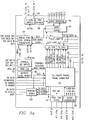
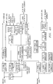
- FIG. 3 there is shown a block diagram of an IC according to the teachings of the present invention. Pertinent elements of this IC will be discussed hereinbelow.
- the IC has three basic modes of operation. Those three modes are an in-circuit emulation mode, a normal mode, and a test mode.
- the in-circuit emulation mode capability is an important aspect of the present invention which will be described in greater detail below.
- the in-circuit emulation mode disables the on-chip microcontroller (designated by reference numeral 40 in FIG. 3), allowing an external in-circuit emulator to be used for software development.
- the normal mode is the mode in which the product containing the IC is operated by the end user. As discussed further below, the normal mode is further subdivided into an active mode and a shut-down mode.
- the final mode of operation, the test mode is basically the same as the normal mode, except that in the test mode it is possible to also enable internal test functions of the IC.
- Entry into the three operating modes is controlled by the state of the reset pin 42 and the tri-level IN1 (TRI1) pin 44.
- TRI1 pin 44 could effect such selection in a number of different ways, one way would be to have the state of the TRI1 pin be monitored and acted upon by the IC when the reset pin 42 goes inactive. If the TRI1 is low, for example, the in-circuit emulation mode could be activated. At a mid supply or no-connect point, the test mode could be activated. Finally, when the TRI1 pin is high and, again, when the reset pin 42 goes inactive, the IC could operate in the normal mode.
- an IC may support an in-circuit emulation mode that disables the on-chip microcontroller 40 allowing an external emulator to function in its place.
- all internal signals that connect to the microcontroller must work with the timing delays inherent in having the microcontroller or emulator off chip.
- the emulation mode is entered at reset if, when the reset pin 42 goes high, the tri-level input 1 pin 44 is low. All internal connections to I/O ports are routed off chip with the exception of the clock connected to the time 0 and time 1 inputs (and it should be noted that this clock can be built externally). ALE and PSEN/ become inputs.
- the clock input to the microcontroller, which is routed off chip is forced on at reset in emulation mode.
- the watchdog timer (element 46 in FIG. 3) does not operate in the in-circuit emulation mode.
- pin 3 functions as an INT0/OUT
- pin 50 functions as an INT1/OUT
- pin 52 functions as a CPUCLKOUT
- pin 54 functions as an ALE input
- pin 56 functions as an RD/input
- pin 58 functions as a WR/input
- pin 60 functions as an ADDR15-8 inputs
- pin 64 functions as high-Z
- pin 66 functions as input
- pin 68 functions as high-Z.
- shut-down there are two power modes, shut-down and active.
- the shut-down mode the 16.432 MHz oscillators (see element 70 in FIG. 1 and element 72 in FIG. 2) and all clocks derived from those oscillators are stopped. All modules are disabled with the exception of the real time clock (which is shown as element 74 in FIG. 3). All analog pins are placed in their OFF state as though the IC was being reset. The real time clock 74 is not affected by the shut-down mode.
- the watchdog timer 46 is disabled in the shut-down mode.
- entry into the shut-down mode is under software control. Entry into the shut-down mode is protected by an access control mechanism to avoid placing the IC in shut-down inadvertently.
- the microcontroller' s clock runs for between 3.56 and 7.2 milliseconds before being stopped. This allows the microcontroller to be programmed to its idle state.
- Wake up from the shut-down mode comes from reset, an any-key-down indication from the keypad scanner, or any non-mask interrupt. All of these conditions cause an interrupt request to be generated.
- the 18.432 MHz oscillator is turned on. Once it becomes stable, the microcontroller clock is turned on at its previously programmed frequency. Once the microcontroller clock is stable, the interrupt request is generated to the microcontroller. This interrupt causes the microcontroller to leave its idle state.
- each module in the IC can be programmably turned on or off via a register.
- These user visible or accessible registers include an address decoder 76, an audio interface 78, a battery level detector 80, a clock generator 82, a codec with an associated ADPCM 84, an interrupt controller 86, a keypad scanner 88, FIFOs 90, the real time clock 74, an RSSI-A/D converter 92, a serial port 94, a logic module 96, a tone ringer 98, a transmitter modem 100, and a reset associated with the watchdog timer 102.
- the audio path in the actually constructed embodiment of the present invention is comprised of the audio interface 78, the codec and associated ADPCM 84, a dual-tone generator (see FIG. 5), and the tone ringer 98.
- the codec, ADPCM, and dual-tone generator functions are implemented with the same digital signal processing (DSP) engine.
- the audio interface 78 connects the analog side of the codec 84 and the tone ringer 98 to the off chip microphone (e.g., element 22 in FIG. 2), ear piece (e.g., element 24 in FIG. 2), speaker (e.g., element 24 in FIG. 2), PSTN (e.g., element 6 in FIG. 2), and so on.
- Software controls the signal routing and amplitudes.
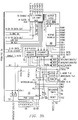
- the audio interface 78 consists of a series of analog inputs, analog outputs, and a multiplexer connecting them, as shown in the block diagram in FIG. 4.
- the various gains, attenuations, and interconnections arising during operation of the embodiment of the present invention shown in FIG. 4 are all software programmable. Each input buffer and output driver can be independently disabled to save power.
- the audio mux has five inputs (two pins 104, 106; a sidetone 108; the tone ringer 98; and a codec D/A 112; three pins 114, 116, 118; and the codec A/D 120).
- the various inputs can be routed to each of the outputs, with some limitations. Possible paths are shown in FIG. 4. The selected inputs are summed at each output.
- a sidetone path is provided from the AI2 input 106 to the A03 output 118.
- the gain is programmable from 0 dB to -42 dB in 3 dB steps.
- pins All and AI2 are analog input pins and pins A01, A02, and A03 are analog output pins.
- the codec portion of the audio path is located between the ADPCM transcoder (heretofore identified as codec/ADPCM 84) and the audio interface 78 (See FIG. 3a).
- the codec portion of the audio path provides a codec function, a DTMF-only mode function, an A-Law test mode function, a loopback 2 function, and a codec/ADPCM enable control function. Each of these functions is discussed briefly in individual paragraphs immediately below.
- the DSP engine has a DTMF-only mode that turns off all DSP functions but the dual-tone generator and those portions of the codec necessary to produce an output DTMF tones. In the actually constructed embodiment of the present invention, this mode is controlled via a bit in the DSP control register.
- A-Law test mode access is provided to the codec function allowing the codec to be tested (analog into A-Law PCM out and A-Law PCM into analog out).
- This test mode breaks the connection between the codec and the ADPCM transcoder, performs linear to A-Law PCM and A-Law PCM to linear conversion, and provides an access point to the 64 kbps A-Law PCM bit stream.
- This test mode is implemented by multiplexing the PCM data I/O and clock functions onto pins normally used for the serial I/O port. In the actually constructed embodiment of the present invention, the data is transmitted and received in eight-bit bursts using a 512 kHz clock.
- loopback 2 With respect to the loopback 2 function, a loopback point is provided connecting the output of the transmit path (input to the ADPCM encoder) to the input of the received path (input point from the ADPCM decoder). Data at this loopback, called loopback 2, is in linear PCM format.
- a single bit located in the clock generator module, is provided for enabling the transmit and receive codec paths. This bit is also used to enable the ADPCM transcoder transmit and receive paths, and the A/D summing amplifier in the audio interface.
- the codec should meet standard CCITT G.714 signal to distortion, gain tracking, frequency response, and idle channel noise specifications.
- the codec module in the actually constructed embodiment of the present invention operates without software intervention.
- the filters, summing points, and attenuators are implemented in microcode executed on the DSP engine.
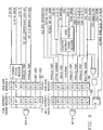
- FIG. 5 there is shown a block diagram of the audio path, excluding the audio interface.
- the audio path is shown to include both a receive path and a transmit path.
- the attenuator/mute 138 is a means to disable the receive path ahead of the voice/tone summing point.
- a programmable attenuator is used so that the signal can be turned off gradually. Muting is accomplished by programming the receive attenuator to an infinite attenuation. Programming minus infinity causes the ADPCM decoder to reset its recursive filters.
- the attenuator is programmed via a receive attenuator register.
- the voice/tone summing point 140 is a point at which the voice and tone signals are summed.
- the low-pass filter 142 is in the actually constructed embodiment of the present invention simply a standard 3400 Hz low-pass filter or the like.
- the interpolator 144 also in the actually constructed embodiment of the present invention, is a series of interpolators to increase the sample rate.
- the D/A converter 146 is a means for converting the signal from digital to analog.
- the transmit path In the transmit path are an A/D converter 148, a decimator 150, a filters and attenuator block 152, and a voice/tone summing point 154.
- the A/D converter 148 is a second order sigma/delta converter or the like which can be used to digitize the input.
- the decimator 150 is hardware which decimates the output of the A/D converter 148.
- the filters and attenuator block 152 includes an attenuator mute, a low-pass filter, a high-pass filter, and a DC reject filter.
- the attenuator/mute portion is a means to disable the transmit path ahead of the voice/tone summing point.
- a programmable attenuator may be used so that the signal can be turned off gradually.
- Muting is accomplished by programming the attenuator to infinite attenuation.
- the attenuator is programmed via a transmit attenuator register.
- the low-pass filter portion of the block 152 is a standard 3400 Hz low-pass filter.
- the high-pass filter portion of the block 152 is a 50/60 Hz rejection filter.
- Such a filter has a programmable enable control, that is, a DSP control register.
- the DC reject filter portion of block 152 removes DC offset. This filter cannot be disabled.
- the voice/tone summing point 154 is a point at which voice and tone signals are summed.
- the test logic interface to the "PCM port” contains a parallel to serial and a serial to parallel shift register pair.
- the interface to the serial I/O port module is serial, with the codec module providing the parallel to serial and serial to parallel conversion, data clock (one eight-cycle burst per frame at 512 kHz), and frame sync clock (8 kHz).
- the DSP control register controls all DSP related functions, including the ADPCM module.
- the ADPCM portion of the audio path provides a full-duplex ADPCM transcoder (linear PCM to ADPCM and ADPCM to linear PCM).
- the transcoder sits between the codec and the FIFOs/B channel I/O.
- the codec and ADPCM have been generally referred to together and with reference numeral 84.
- a test mode allows A-Law encoding and decoding to be added to the signal path for compatibility testing.
- a test mode is provided allowing access to the ADPCM portion of the audio path.
- This allows the ADPCM transcoder to be tested independent of the audio interface and filters (A-Law PCM into ADPCM out and ADPCM into A-Law PCM out).
- This mode breaks the connection between the codec and the ADPCM transcoder, providing a connection point for a 64 kbps A-Law PCM bit stream.
- the test mode is implemented by multiplexing the PCM data I/O and clock functions onto pins normally used for the serial I/O port (the B/D channel I/O port is used for the 32 kbps ADPCM connection).
- a single programming bit is provided for enabling the DSP and audio interface. This bit is the same bit that is used to enable the codec transmit and receive paths, and is located in a module enable control register 0.
- the actually constructed embodiment of the present invention complies with CCITT G. 721 bit-for-bit.
- the ADPCM transcoder function is microcode executed by the DSP engine. It should be noted that the input to the encoder and the output from the decoder is in linear format (not compounded PCM because the A-Law compression and expansion blocks are not used in normal operation).
- the ADPCM module connects to the FIFO/B channel data multiplexer.
- the input to the decoder and output from the encoder is in four-bit nibbles.
- the data routing on the codec side reference should be made to the block diagram of the audio path, FIG. 5.
- the loopback 2 and test mode switches are controlled via the DSP control register, discussed in the Audio Path--Codec section above.
- a tone generator capable of generating two simultaneous tones is used in the actually constructed embodiment of the present invention.
- the output of the generator is individually summed into the transmit and receive paths, with independently controlled amplitudes.
- the transmit and receive paths feeding the summing point can be muted, allowing only the tones to be output.
- the tone generator may be seen to consist of a tone 1 generation block 156, a tone 2 generation block 158, a receive path tone attenuator 160, and a transmit path tone attenuator 162.
- tone 1 and tone 2 generators 156, 158 the interface to each of these generators consists of four bytes of programming, three that specify the frequency and one that specifies the amplitude.
- Writing the tone 2 amplitude register causes all eight bytes to be loaded into the DSP, thus changing the tones. This also starts the tone generation.
- the tone generation is terminated by writing the zero amplitude value to the desired amplitude register (to turn off tone 1, the tone 1 amplitude register must be written with the zero amplitude coefficient, followed by a write to the tone 2 amplitude register to trigger the update of all 8 registers).
- Each of the two tone generators 156, 158 operates independently.
- the outputs of the two tone generators 156, 158 are summed together.
- the combined signal sums into the receive and transmit speech paths via the two attenuators 156, 158.
- the transmit and receive speech signals pass through their own programmable attenuators 164, 166 prior to reaching the summing point. This allows independent adjustment of the relative tone/speech levels for the transmit path and the receive path.
- the tone ringer (element 98 in FIGs 3a and 4) is capable of generating multiple single frequency sequential square wave tones with minimal transients when switching between frequencies.
- the tone ringer function is capable of operating whether the codec/ADPCM 84 function is enabled or disabled.
- the tone ringer hardware consists of a tone ringer frequency register, a tone ringer amplitude register, a counter/divider, and an attenuator.
- the tone ringer 98 consists of a programmable eight-bit polynomial counter and associated control logic.
- the input clock is 288 kHz.
- the output feeds the tone ringer input buffer/attenuator located in the audio interface module.
- a control bit located in the clock generator module turns the tone ringer 98 on and off by starting and stopping the clock. This bit also disables the tone ringer attenuator and buffer.
- the system control functions in the cordless telephone application of the present invention which is described herein are performed by the microcontroller 40, the clock generator module 82, the address decoder module 86, the interrupt controller module 86, the watchdog timer/reset module 46, a parallel port module 168, a serial port module 94 (see FIG. 3a), a keypad scanner functions module 88 (see FIG. 3b), a real-time clock module 74 (see FIG. 3a), and a battery level detector module 80 (see FIG. 3a).
- an 8-bit microcontroller providing the functions of the 80C32T2 member of the 80C51 family of Advanced Micro Devices (AMD) products is integrated on-chip. It may be noted, however, that a few functions of the 80C32T2 are not implemented on the IC. For example, the oscillator function of the 80C32T2 is replaced by a clock input and the reset generator of the 80C32T2 is replaced by a reset input. Additionally, the external address select (EA/) is internally tied low, selecting off-chip ROM. In addition to the microcontroller, additional RAM as well as a demultiplexed form of the address bus is provided.
- the PSEN/pin assumes a high impedance state.
- Port O it is used in connection with multiplexed address/data bus bits 7-0.
- Port 1 is used for general I/O lines. These lines are mapped to specific control functions by software.
- the Port 1 I/O lines contain a weak pull-up. Disabling the weak pull-up is accomplished by setting a corresponding port control register bit (PCRB) to an appropriate value. After RESET, the Port 1 weak pull-ups are enabled. During emulation mode, the weak pull-ups are disabled and the port pins assume a high impedance state.
- PCB port control register bit
- Port 2 is used for address lines 15-18.
- the Port 2 I/O lines contain a weak pull-up. Disabling the weak pull-up is accomplished by setting a corresponding port control register bit (PCRB) to an appropriate value. After RESET, the Port 2 weak pull-ups are enabled. During emulation mode, the weak pull-ups are disabled and the port pins assume a high impedance state.
- PCB port control register bit
- P3.0 is used as either the microcontroller serial port receive data input (RxD) or as a general purpose I/O pin.
- P3.1 is used as either the microcontroller serial port transmit data output (TxD) or as a general purpose I/O pin.
- P3.2 is used internally as an interrupt input from the internal interrupt controller (INT0/).
- P3. 3 is used internally as an interrupt input from the internal interrupt controller (INT1/).
- P3. 4 is used as the internal timer 0 clock input. This pin is not available external to the IC.
- P3. 5 is used as the internal timer 1 clock input. This pin is not available external to the IC.
- P3. 6 is the WR/ strobe for the address/data bus.
- P3. 7 is the RD/ strobe for the address/data bus.
- the Port 3 I/O lines contain a weak pull-up. Disabling the weak pull-up is accomplished by setting a corresponding port control register bit (PCRB) to an appropriate value. After RESET, the Port 3 weak pull-ups are enabled. During emulation mode, the weak pull-ups are disabled and the port pins assume a high impedance state.
- PCB port control register bit
- the Port 1, 2, and 3 I/O buffers are capable of disabling the weak p-channel pull-up through software control.
- the necessity of this function permits the buffers to eliminate current sourcing when the buffer is driven low by an external signal.
- this weak pull-up disabling feature of embodiments of the present invention eliminates undesirable power consumption increases.
- the AMD 80C32T2 lacks such a mechanism. After reset, all of the Port 1, 2, and 3 I/O buffers are held "high" by the weak pull-up. This state is functionally compatible with the 80C32T2 microcontroller.
- the software must first disable each bit by configuring the port pin with the corresponding port control register bit.
- the corresponding port control register bit resides at the same address as the port SFR bit.
- Port 1 resides at SFR memory location 90H.
- the Port 1 control register also resides at SFR memory location 90H. Modification of the Port 1 Control Register is only accomplished when the PCRA bit in the PCFIG SFR is set to a "1". When the PCRA bit is cleared, an operation to the Port SFR address results in the Port SFR getting updated.
- Port 0 Since only Ports 1, 2 and 3 contain weak pull-ups, Port 0 is exempt from this feature.
- PCRB PORT BIT FUNCTION 0 0 Drives a "0" output, no pull-up (80C51 compatible) 0 1 Drives a "1" for 2 cycle, weak pull-up is on. (80C51 compatible) 1 0 Drives a "0" output, no pull-up 1 1 Input only, (no pull-up, high impedance input)
- the PCRA bit Upon power-up, the PCRA bit is disabled and any writes to the ports result in the port SFR being updated. Once the PCRA bit in the PCFIG register is set, it becomes possible for each port bit to have the weak p-channel device turned off. After each port bit is appropriately configured, the user must clear the PCRA bit before writing to the ports.
- the port pin may not return to a "1" immediately. This condition is similar to the 80C51 when an external device drives the input signal low and then allows the pin to "float” back to a "1". This rise time of the signal is dependent on the loading of the pin and may take several microseconds to return to a stable "1".
- the 80C32T2 has 256 bytes of RAM located in the "Internal Data RAM” space. 1024 bytes of additional "on-chip” RAM is located in “External Data RAM” space. All of the 1024 bytes of on-chip RAM is backed up by the real-time clock's back-up battery. The backed up RAM can support read and write accesses down to 2. 2 Volts. The backed up RAM can retain data down to 1. 8 Volts.
- interrupt enable during shut-down in the actually constructed embodiment of the present invention, if the IC is in a shut-down mode and the microcontroller is in an idle mode, the condition of the microcontroller' s interrupt mask bits (TCON register bits 7, 2, and 0) is ignored, enabling the INT0/ and INT1/ interrupts. The actual TCON bits are not changed to safeguard against the IC entering a shut-down mode with interrupts disabled.
- the ALE I/O pin is multiplexed with the general output bit 9.
- the INT0/OUT and INT1/0UT pins are multiplexed with the external I/O 0 and external RAM chip select outputs, respectively, from the address decoder module 76. During the in-circuit emulation mode, these pins always provide the ALE-OUT, INT0/, and INT1/0UTPUT functions.
- the ALE pin can be either ALE OUT or general output 9. Selection is programmed in the address decoder module. The INT0/ and INT1/ pins are always used as chip select outputs in normal operation.
- a demultiplexed form of the 80C32T2' s address bus is constructed by latching the low-order address byte, providing the LATCHED ADDRESS 7-0 pins. The address is latched off of the A/D 7-0 bus on the falling edge of ALE.
- internal timing accounts for the delays associated with bringing A/D 7-0 and ALE on chip when the IC is in in-circuit emulation mode.
- PO. 7-PO. 0 is the microcontroller I/O port 0. This port provides the multiplexed D7-0 and A7-0 bus.
- the pins When the IC is in reset the pins are held weakly high. In shut-down, the pins will either be held strongly low or weakly high. In in-circuit emulation mode the pins are high impedance.
- P1. 7-P1. 0 is the microcontroller I/O port 1. This port provides the eight general purpose I/O pins associated with the parallel port module. When the IC is in reset the pins are held weakly high. In shut-down, the pins hold their programmed state. In in-circuit emulation mode the pins are high impedance.
- P2. 7-P2. 0 is the microcontroller I/O port 2. This port provides the high order eight bits of the address bus (A15-8). When the IC is in reset or shut-down, the pins are held weakly high. In in-circuit emulation mode the pins are high impedance.
- P3. 7 is the microcontroller I/O port 3. 7. This pin provides the microcontroller RD/ (read, active low) strobe. In in-circuit emulation mode the pin is high impedance. In shut-down or during reset the pin is held weakly high.
- P3. 6 is the microcontroller I/O port 3. 6. This pin provides the microcontroller WR/ (write, active low) strobe. In in-circuit emulation mode the pin is high impedance. In shut-down or during reset the pin is held weakly high.
- P3. 1 is the microcontroller I/O port 3. 1. This pin provides the microcontroller' s internal serial port transmit data output. The pin can also be used as a general purpose I/O port. In in-circuit emulation mode the pin is high impedance. In reset the pin is held weakly high. In shut-down the pin holds its programmed state.
- P3. 0 is the microcontroller I/O port 3. 0.
- This pin provides the microcontroller' s internal serial port receive data input.
- the pin can also be used as a general purpose I/O port. In in-circuit emulation mode the pin is high impedance. In reset the pin is held weakly high. In shut-down the pin holds its programmed state.
- PSEN/ is the program store enable. When active, the address on ports 0 and 2 pertains to code space. PSEN/ is placed in a high impedance state in in-circuit emulation mode, and is an output in normal mode. In reset, PSEN/ is held weakly high. In shut-down the pin is held strongly high.
- ALE is the address latch enable. This signal is used to latch the address off of the A/D 7-0 bus. ALE is high impedance during in-circuit emulation mode. ALE is an output, multiplexed with OUT9 during normal mode. In shut-down or reset the pin is held strongly high.
- LATCHED ADDRESS 7-0 is the output of the address latch, providing the non-multiplexed LA7-0 bus. At reset, shut-down, and in in-circuit emulation mode these pins are driven strongly.
- the clock generator 82 (see FIG. 3a) provides the crystal oscillator, power mode control, module enable control, and clock dividers for the IC.
- the IC is placed into shut-down mode by setting a bit in a shut-down/microcontroller clock control register. After the bit is set the oscillator 72 continues to run for 3. 56 - 7. 12 milliseconds in order for software to place itself in its idle mode, then all clocks, including the CPUCLK are stopped. In the actually constructed embodiment of the present invention, the IC terminates the shut-down cycle if an interrupt is received after the enable bit is set, and before the CPU clock is stopped.
- shut-down/microcontroller clock control register access to the shut-down/microcontroller clock control register is protected by an interlock mechanism to reduce the risk of accidental clock stoppage due to software problems.
- This mechanism requires the software to write to a special access control register, and then write the shut-down/microcontroller clock control register. This double-write procedure must be done twice before the clock speed control register is updated.
- Wake-up comes from reset, an any-key-down indication from the keypad scanner 88, the real-time clock interrupt (if not masked within the real-time clock 74), or any non-masked interrupt.
- the oscillator is re-started. A delay of approximately 3.56 milliseconds is required for the oscillator to stabilize. After this delay, the microcontroller 44 and watchdog timer 46 clocks are re-started. The microcontroller clock re-starts at the previously programmed rate.
- the keypad any-key-down and real-time clock interrupts are enabled, even if the associated interrupt enable bits are cleared, i.e., even if the interrupts are disabled.
- the actual interrupt enable bits are not changed.
- the real-time clock interrupts can still be masked within the real-time clock module 74 in the actually constructed embodiment of the present invention.
- the actually employed microcontroller clock has a programmable divider with an input of 18. 432 MHz.
- the programmable rates are divided by 2, 4, 8, 16, 32, 64, 128, and 256.
- the CPU clock returns to the speed programmed in the control register.
- the CPUCLK can be turned off by placing the IC in shut-down mode.
- the transition to the new frequency is accomplished without producing clock pulses that violate the 80C32T2, or other such appropriate product, data sheet timing specifications.
- the microcontroller clock also has a selectable automatic speed-up mode. If the automatic speed-up option is selected, all interrupts force the microcontroller clock divider to the divide by two state. After the clock is sped-up, it will remain at the divided by two frequency until the speed is reprogrammed to a lower value. No illegally short pulses are allowed at the frequency transition point.
- the processor clock continues to run for between 3. 56 and 7. 12 milliseconds before being stopped.
- the clocks to each module are provided by the clock generator module 82. Control bits are provided to allow software to turn on and off specific modules. When a module is turned off, its clock is stopped and held low.
- the serial port 94 supports data rates of 288 kHz, 144 kHz, and 36 kHz.
- the clock provided to the serial port module is divided down to the desired data rate by the clock generator module 82.
- the clock speed is selected via the serial port timing control register.
- the serial port module and this clock are enabled via a module enable control register 0. When the module is disabled, the clock is stopped low.
- FIG. 7 is a block diagram of the clock generator module.
- the clock generator module directly or indirectly comprises the oscillator 70, shut-down mode control logic 170, microcontroller clock control logic 172, module enables 174, and a module clock divider 176. Each of these is described further in an individual paragraph immediately below.
- the oscillator 70 is designed to run at 18. 432 MHz, using a parallel resonant mode crystal. Start-up capacitors are required; however, the actually constructed embodiment minimizes capacitance value to save power.
- the shut-down mode/microcontroller clock control logic 170, 172 controls the entry into shut-down, microcontroller clock frequency, and automatic speed-up.
- register bits to turn on and off specific modules within the IC are located in the clock generator module 82. These bits also stop the clock outputs to their respective modules.
- the module clock divider logic 176 is a divider chain that produces the clock frequencies required by each module.
- the clock generator module 82 has three pins.
- Pin MCLK XTAL is the master clock crystal pin 1. This pin is for input and is on the input side of the oscillator 70.
- the oscillator 70 is designed to work with either a parallel resonant crystal or an external logic level input.
- the MCLK XTAL 2 pin is the master clock crystal pin 2. This pin is for output and is on the output side of the oscillator 70. If a crystal is used, this pin is connected to the crystal. If an external logic level signal is used, this pin is left unconnected.
- the CPUCLKOUT pin is connected to the same clock that feeds the microcontroller 40. It is an output that can be routed off chip. In in-circuit emulation mode, the CPUCLKOUT is always active.
- this clock is multiplexed with the CSOUT2/ signal from the parallel I/O port module.
- the multiplexer control is located in the address decoder module 76 (see FIG. 3b). In reset, this pin defaults to the CSOUT2/ function, and is held high. At shut-down, if the pin is programmed for CPUCLK operation it is held low.
- the actually constructed clock controller module 82 contains the following programmable registers: a shut-down/microcontroller clock control register; a shut-down/microcontroller clock access; a protection register; a module enable control register 1; a module enable control register 2; and a serial port timing control register.
- the addresses of all internal registers as well as the on-chip RAM and the three external chip selects are decoded by the address decoder module 76. Enable signals are generated when internal registers or internal RAM is accessed by the microcontroller. Chip selects outputs are generated when external RAM space or either of the two external I/O spaces are accessed.
- the actually constructed address decoder module 76 includes a CSOUT0/pin, a CSOUT1/pin and a CSOUT2/pin.
- the CSOUT0/pin carries a signal which is multiplexed with the INT0/OUT signal. This pin also provides the chip select function when the IC is not in in-circuit emulation mode.
- the CSOUT0/signal is active (low) when a MOVX instruction is executed to the external I/O 1 space. In reset or shut-down this pin is held high.
- the CSOUT1/pin carries a signal which is multiplexed with the INT1/OUT signal. This pin also provides the chip select function when the IC is not in in-circuit emulation mode.
- the CSOUT1/ signal is active (low) when a MOVX instruction is executed to the external RAM space. In reset or shut-down this pin is held high.
- the CSOUT2/pin carries a signal which is multiplexed with the CPUCLKOUT signal. This pin also provides the chip select function when the IC is not in in-circuit emulation mode and the CSOUT2/ enable bit is set in a chip select control register.
- the CSOUT2/ signal is active (low) when a MOVX instruction is executed to the external I/O 2 space. In reset, this pin is held high. If the pin is programmed for CSOUT2/ mode, it is held high in shut-down.
- the aforementioned chip select control register is the only user visible register in the address decoder module 76.
- the actually constructed address decoder module 76 includes an address latch and an associated pin.
- the address latch provides the latched form of the low order eight address bits (LADDR 7-0).
- the latched address bus (LADDR 7-0) pins are outputs when the IC is in normal, shut-down, or in-circuit emulation modes. When the IC is in shut-down, the pins are driven strongly with the last value before entering shut-down. The outputs change on the falling edge of ALE.
- the interrupt controller 86 gathers interrupt requests from various sources internal and external to the IC and generates an interrupt to the microcontroller 40 (INT0/ and INT1/).
- the interrupt system employed in the actually constructed embodiment of the present invention has a multilevel structure, including interrupt causes and status registers, a local mask, a local interrupt source register, a main interrupt mask register, and a main interrupt source register. Each of these elements is discussed further in an individual paragraph immediately below.
- interrupt causes and status registers With regard to interrupt causes and status registers, the causes of the interrupts form the lowest level, and are local to each module. These causes can be inputs to pins, conditions such as empty or full data buffers, and the like. The causes are reported in "status registers". A status register, when read by software, always returns the current state of cause signal (for example, the current logic level on an input pin). The bits in a status register are not affected by interrupt masking.
- the cause signals are ANDed with associated mask signals from an "interrupt mask register".
- the output of these AND gates connect to a "local interrupt source register".
- the mask register is located in the module that contains the associated cause signals.
- the local interrupt source register is used by software to determine the cause of an interrupt.
- the bits in the interrupt source register can be set by either rising edge, falling edge, or both edges of the non-masked cause signal.
- the bits in interrupt source registers are cleared separately from each other. In general, each bit is cleared when software responds to the cause. This response can be reading a receive buffer, reading an input port status register, or the like.
- the outputs of each of the register bits is ORed together to produce one interrupt request signal. This signal is sent to the interrupt controller module.
- the source register is located in the module that contains the associated cause signals.
- the interrupt request signals are ANDed with associated mask signals from the "main interrupt mask register" (located in the interrupt controller module 86).
- the output of these AND gates connect to a "main local interrupt source register".
- the main interrupt source register is used by software to determine the cause of an interrupt.
- the bits in the interrupt source register reflect the logic level of the interrupt request signals, provided they are not masked. In general, each interrupt request is cleared when software responds to the specific interrupt cause.
- the outputs of the main interrupt source register are ORed together and forwarded to the microcontroller.
- FIG. 8 shows the structure of the interrupt controller 86.
- Interrupt requests from the logic module 96 see FIG. 3a
- external interrupt inputs such as hookswitch/lock-ups
- the serial I/O 94 the parallel I/O (see FIG. 13 and the accompanying discussion)
- keypad scanner 88 and the real-time clock 74 modules feed the two main interrupt source registers 178, 180.
- a master interrupt mask function is provided in the microcontroller in the form of a main mask register 0 182, and a main mask register 1 184.
- Figure 9 shows the structure of the status, mask, and source registers necessary to handle interrupt cause signals from the logic module 96.
- the interrupt controller module 86 is comprised of seven user-accessible registers: a main interrupt source register 0 186; a main interrupt mask register 0 188; a main interrupt source register 1 190; a main interrupt mask register 1 192; a D-channel status register 194; a CHM/SYNC mask register 196; and a CHM/SYNC interrupt source register 198.
- the interrupt controller 86 includes an INT0/OUT pin, and an INT1/OUT pin.
- the INT0/OUT signal is an output from the interrupt controller 86 to the microcontroller 40. It is routed off-chip via the INT0/OUT pins. It is used only in in-circuit emulation mode. When the IC is not in in-circuit emulation mode, this pin is used for the chip select zero (CSOUT0) output.
- the INT1/OUT pin carries a signal which is an output from the interrupt controller 86 to the microcontroller 40. It is routed off-chip via the INT1/OUT pin. It is used only in in-circuit emulation mode. When the IC is not in in-circuit emulation mode, this pin is used for the chip select one (CSOUT1) output.
- User accessible registers in the interrupt controller module include the main interrupt source register 0 186; the main interrupt source register 1 190; the main interrupt mask register 0 188; the main interrupt mask register 1 192; the D channel status register; the CHM/Sync interrupt source register 198; and the CHM/Sync mask register 196.
- the watchdog timer 46 detects if the microcontroller software becomes hung-up or lost, and generates a hardware reset to the IC as well as the rest of the system. A hardware reset is generated if an internal counter is not cleared every two seconds. The counter is cleared by the microcontroller 40 writing a specific code sequence to an internal watchdog key register. It should be noted that the watchdog timer 46 is not operational in shut-down or in-circuit emulation modes.
- Figure 10 is a state diagram of the watchdog timer and the reset output mechanism.
- the actually constructed watchdog timer 46 generates a 1. 78 ms pulse on the RESET/ (active low) pin if it times out.
- Hardware internal to the IC is also reset by a watchdog timer time-out; the result is identical to activating the RESET/pin.
- the time-out value is approximately 1. 78 seconds.
- a specific key sequence must be written to the aforementioned internal watchdog key register within this 1. 78 seconds after reset, and within 1. 78 seconds of the previous update, to prevent time-out.
- the key sequence is a two stage function starting from reset.
- the watchdog timer 46 starts in stage one, waiting for a write to the watchdog key register. If the value written to the watchdog key register is anything but an ASH, a system reset is generated (just as if the terminal count had been reached). If the write was an A5H, stage two is entered. In stage two, the watchdog timer 46 waits for another write. If the write is a 5AH, the timer is reset and stage one is re-entered. If the write is something other than a 5AH, a system reset is generated.
- FIG 11 shows the organization of the watchdog timer used in the actually constructed embodiment of the present invention.
- the timer chain comprises a two second counter 200 and a two millisecond pulse generator 202.
- a 1 kHz clock is received from the clock generator module 82 and fed to the disable control block.
- the clock output signal feeds the two millisecond pulse generator 202 and the two second counter 200.
- the terminal count output of the two second counter 200 is fed to the pulse generator 202 to initiate the generation of a two millisecond pulse.
- the watchdog key mechanism consists of a user visible register 204 and a state machine 206.
- the user visible register 204 is written periodically by software to indicate that the software is functioning normally.
- the state machine 206 verifies that the register is updated correctly, generating a clear strobe to the two second counter 200 if all is well, and an error strobe to the two millisecond counter 202 if the register is updated incorrectly.
- the watchdog key register 204 is the access point where software clears the watchdog timer 46. A sequence of two writes is required to clear the timer 46. In the actually constructed embodiment of the present invention, this sequence must be performed every two seconds to prevent the generation of a system reset.
- the actually constructed parallel I/O port consists of the micro-controller port 1 interrupt structure, a 11-bit general purpose output latch, 2 tri-level input pins, and three external interrupt inputs.
- the RxD and TxD pins in microcontroller port 3 can also operate as general purpose I/O ports. These ports are organized as discussed immediately below.
- maskable interrupts are programmably generated on one edge of each pin.
- the pins are divided into three separate interrupt source registers, one for P1. 7-4, one for P1. 3-2, and one for P1. 1-0.
- the general purpose outputs are programmed via the general purpose outputs registers 0 and 1.
- the outputs all default high.
- the two tri-level input single pins can report three input states, high, low, or open. Typical applications are dial type selection and factory test mode selection. Additionally, as discussed in considerable detail above, TRI-LEVEL IN1 is used to select in-circuit emulation mode.
- three input pins are provided that generate interrupt requests on both rising and falling edges. These pins can be used for hookswitch, channel synthesizer lock-up, and modem synthesizer lock-up inputs.
- FIG. 12 shows the basic structure of the interrupt function.
- the output latch provides 11 general purpose output pins for controlling external functions.
- This is a simple pair of registers (one 7-bit and one 4-bit) residing on the microcontroller data bus. When a bit is set in one of the registers (by software), the corresponding output pin is also set. When the bit is cleared, the pin is cleared. All pins that provide one of the general purpose outputs as their default state, default to a high level.
- the multiplexing control for all pins except the keypad (OUT 6,7) and tri-level input (OUT 10) is located in the module where their other function originates, not in the parallel port module (designated by reference numeral 208 in FIG. 12).
- the keypad and tri-level multiplexing is controlled in general purpose output register 1.
- two pins are provided that can detect three distinct input states: high, low, and open, or no connect.
- the state of the input is reported in an external interrupt status register. These pins do not generate interrupt requests.
- the TRI-LEVEL IN1 pin is used primarily for selecting the operating mode of the IC after the RESET pin goes inactive.
- the TRI-LEVEL IN1 pin can be used as a general input in slight variations of the actually constructed embodiment of the present invention, but extreme care should be taken since a reset could cause the IC to enter the in-circuit emulation mode.
- three interrupt inputs are provided that generate interrupt requests on both rising and falling transitions.
- the status of each input pin is reported in a separate one-bit register. If a pin changes state since the last time its status register was read or reset, an interrupt request is latched and sent to the interrupt controller module. Reading the source register clears the latch and thus the interrupt request.
- the 11 outputs are independently controlled by their respective bits in the general purpose output control registers 0 and 1. Further, the input pins are pulled to mid-supply (Vcc/2) by pull-up and pull-down resistors when read. The pins each feed a separate pair of comparators. One is biased to produce a high at its output if the input is high, and one is biased to produce a high at its output if the input is low. If the input is open, both comparators output a low state. Still further, it may be noted that the pin logic should be designed to disable the pull-up and pull-down resistors when the state of the pin is not being evaluated. This is a power saving feature.
- the maximum resistance of the external input with respect to Vcc or Vss is 50 Ohms (when the input is high or low). The maximum capacitance is 50 pF.
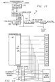
- FIG. 13 there is shown a more detailed view of the external interrupt input structure. It may be seen therein that this structure comprises three input pins 220, 222, 224, three status registers 226, 228, 230, and three transition detector latches 232, 234, 236.
- the three external interrupt input status registers 226, 228, 230 which are one-bit registers, report the current status of the external interrupt input pins 220, 222, 224.
- the status bit changes as the pins change. Reading one of the registers clears the associated transition detector latch 232, 234, 236.
- the output of each latch 232, 234, 236 is fed to the interrupt controller module 86 where it is ANDed with an enable bit.
- the serial interface is a combination of four serial channels. In the actually constructed embodiment of the present invention, these channels provide communication with frequency synthesizers, an LCD controller, an EEPROM, and a PCM codec test equipment.
- a combined set of transmit, receive, and clock logic is used to support the synthesizer, LCD, EEPROM, and PCM interfaces (see FIG. 14 wherein the transmit, receive and clock logic are generally designated by reference numerals 240, 242 and 246, respectively). This combined set of hardware is referred to as the SI/O interface.
- a serial interface is provided for communicating between the on-chip microcontroller and an NEC ⁇ PD7225 LCD controller IC, or the like. This is also a one direction interface, with communication going only from the IC to the LCD controller.
- the actually constructed EEPROM interface is bidirectional, and is compatible with 8- and 16-bit devices that support the National, General Instruments, Exel interface. Additionally, support for devices that output data on the falling edge of the clock is required. Thus, for compatibility with a wide variety of devices, the port can be programmed to receive data on the rising or falling edge.
- codec test mode the Data In pin becomes the 64 kbps codec receive input
- Data Out pin becomes the 64 kbps codec transmit output
- Clock pin becomes a gated 512 kHz PCM data clock output (bursts of eight cycles at the 8 kHz frame rate).
- the Data In pin becomes the 64 kbps ADPCM transmit input (PCM data input)
- the Data Out pin becomes the 64 kbps ADPCM receive output (PCM data output)
- the Clock pin becomes the 512 kHz PCM data clock output (eight bit bursts at the 8 kHz frame rate).
- the B/D channel port provides the 8 kHz frame sync clock.
- the 64 kHz data clock must be synchronized to the 8 kHz frame sync.
- the actually constructed PCM test port does not use the serial I/O port' s transmit buffer, receive buffer, or clock generator.
- the audio path logic provides the clock and a serial transmit bit stream, and receives the receive data in serial form.
- the PCM test function uses the serial I/O port pins, but the logic to support clock generation, clock synchronization, serial to parallel, and parallel conversion is handled within the audio path logic.
- the actually constructed keypad scanner provides the ability to support keypads of up to 36 keys. This keypad scanner operates in two modes: 1) activity detect, and 2) normal.
- the activity detect mode it is not necessary to determine which key is depressed, only that a key has been depressed. This allows the IC to wake up from shut-down mode when the user presses a key. An output is generated to the clock generator module 82 when activity is detected while the IC is in shut-down mode.
- an interrupt is generated when activity is detected, e.g., when a key is closed.
- the user responds to the interrupt by masking the keypad interrupt, setting a microcontroller timer (debounce time is typically 4 to 16 milliseconds), and returning from the interrupt.
- a microcontroller timer debounce time is typically 4 to 16 milliseconds
- an interrupt is generated.
- FIG. 15 shows a block diagram of the keypad scanner.
- the module is comprised of the scanner unit 250 and the keypad status register 252.
- the scanner 250 contains row and column input pins and comparators, and a block of logic 254 that detects the no keys down, multiple keys down, and any key down conditions.
- the status logic formats the inputs from the scanner, and presents this status to the user. More specifically, keypad status logic comprises the following: Inputs
- a real-time clock is provided on the actually constructed IC.
- This clock 74 (see FIG. 3a) operates from the normal IC supply while the IC is powered on, and from a dedicated battery when the IC is powered down.
- a 32. 768 kHz crystal is connected to the real-time clock.
- a 1k byte block of RAM is provided.
- This "on-chip" RAM is independent from the real-time clock except that it is powered from the real-time clock's BATT IN pin.
- Figure 16 show a block diagram of the actually constructed real-time clock module 74.
- the actually constructed IC includes a mechanism providing a digital representation of the power supply (i.e. battery) voltage level over a range of 2.7 to 5.5 volts.
- the power supply i.e. battery
- the battery voltage monitor circuit compares the voltage on a Vcc pin to an internal threshold voltage. If Vcc is above the threshold voltage, the comparator output is high. If Vcc is below the threshold, the comparator output is low.
- the internal threshold voltage is programmable via a 4-bit code from 2.7 Volts to 5.4 Volts, with an accuracy of ⁇ 5%.
- FIG. 17 is a block diagram of the actually constructed battery level detector module.
- the CT2 portion of the IC's accordi ng to the teachings of the present invention includes the following modules: FIFOs 90, a B/D Channel Port (see FIG. 3b), a transmit modem 100, an RSSI A/D Converter 92, and a logic module 96.
- two unidirectional FIFOs 260, 262 are provided between the ADPCM block 84, the B channel I/O 264, and the frame formatter 96, with one in the transmit direction and one in the receive direction 262 (see FIG. 18).
- These FIFOs provide an elastic store between the 72 kbps radio burst rate and the constant 32 kbps ADPCM, B channel port rate.
- the FIFOs appear to be serial when viewed from the frame formatter 96, and 4 bits wide when viewed by the ADPCM block 84 because the ADPCM operates on nibbles.
- the actually constructed FIFO module 90 builds 512 kHz, 32 kHz, and 8 kHz clocks from either a 1. 152 MHz clock from the logic module 96, (specifically, a PLL1152) or a fixed 1. 152 MHz clock from the clock generator module 82.
- the actually constructed B/D Channel I/O Port module 264 provides six I/O pins that are multiplexed to serve four separate functions: a B channel I/O port, including encryption; a D channel I/O port; a single transmit (Tx Modulator I/O); and six general purpose output ports.
- the transmit modulator 100 accepts serial data from the CT2 logic module 96 and converts it to a quadrature pair of single-ended analog outputs.
- the outputs generated in the actually constructed embodiment of the present invention are intended to be externally mixed with an IF carrier and summed to obtain the desired frequency modulated signal.
- FIG. 19 A block diagram of the modulator 100 is shown in FIG. 19.
- the heart of the modulator 100 is a look-up ROM 270 addressed by a data dependent state machine address generator 272 and followed by a series of synchronizing latches 274.
- Two identical 6-bit + sign DAC's followed by buffers drive the analog outputs.
- test mode is provided in embodiments of the present invention to simplify spectral measurements.
- the receive signal strength indication (RSSI) module 92 provides a digital representation of the RF receive signal level. Functionally, current to voltage translation, input range, and microprocessor access of the RSSI A/D converter are noteworthy. With respect to current to voltage translation, an external FSK demodulator generates an analog signal that' s current is proportional to the receive signal strength. This output current is terminated in an external resistor to translate it into a voltage. With respect to input range, the input range of the A/D converter is determined primarily by the common mode voltage swing of the input comparator.
- the A/D converter must be enabled (e.g., via a bit in a module enable control register in the clock generator module) and a conversion must be requested. Requests can be made via software.
- a frame controller which comprises a receive timing recovery, a frame timing generator, a SYNC channel handler, a B channel handler, a D channel handler, and a modem timing adjustment.
- FIG. 20 is a block diagram of the frame controller, including the receive timing recovery, frame timing generator, SYNC channel handler, B channel handler, D channel handler.
- bit synchronized timing from the receive data (Rx Data) is generated and fed to the various functions.
- the SYN channel handler receives a burst signal and the PLLed clock from the receive clock generator (DPLL) and it gives received sync information to the frame timing generator and the CPU. It also receives transmit timing pulses from the frame timing generator, transmit data from the B channel handler and the D channel handler and it generates a transmit burst signal.
- DPLL receive clock generator
- the frame timing generator receives received synchronization information from the syn channel handler when the system is receiving a signal, gives all the necessary receive and transmit timing pulses to the B channel handler, the D channel handler, the SYN channel handler of the transmit portions, MODEM timing adjustment, and any other blocks where those pulses are required.
- the modem timing adjustment measures the delay of the modem and the RF section when they are transmitting and receiving a reference signal from the modem.
Landscapes
- Engineering & Computer Science (AREA)
- Computer Networks & Wireless Communication (AREA)
- Signal Processing (AREA)
- Mobile Radio Communication Systems (AREA)
- Telephone Function (AREA)
Abstract
Description
- This application is related to the following copending US and equivalent European Patent Applications filed today:
US Application No European Patent Application No Our Reference 07/917,497 HRW/TT0139/BEP 07/917,489 HRW/TT0140/BEP 07/917,488 PCCS/TT0141/SMP 07/917,503 PCCS/TT0142/SMP 07/918,626 PCCS/TT0144/SMP 07/918,625 PCCS/TT0145/SMP 07/918,624 PCCS/TT0146/SMP 07/918,631 HRW/TT0147/BEP 07/918,632 PCCS/TT0148/SMP 07/918,622 PCCS/TT0149/SMP 07/918,621 PCSS/TT0150/SMP - All of the related applications are hereby incorporated herein in their entirety by this reference thereto.
- The present invention relates to integrated circuits (IC's), such as IC's involved with the speech, control channel, or microcontroller portions of a modem, or with the man-machine interface functions of a cordless telephone.
- The standard telephone consists of a base unit and a handset unit connected to each other by an electrical cord. The base unit itself is connected by another cord to a receptacle on a wall, telephone pole or a similar immovable structure to which the telephone network line extends. Because of this connection to an immovable structure, the range of movement of the operator of the telephone is quite limited. Even when the cords connecting the handset unit to the base unit and the based unit to the wall are long, it can be cumbersome either to move the entire telephone around to make calls from difference locations or to walk around with the handset unit once a call has been placed. The simple fact that there is always a continuous physical connection between the person making the phone call and the immovable wall or other fixed structure can be a great inconvenience.
- The cordless telephone represents a significant improvement over the standard telephone. In the conventional cordless telephone, the base unit is still connected to the receptacle on the immovable wall or the like by a cord so that message signals from the telephone network line may be received and transmitted. However, the handset unit of the cordless telephone is an independently operative unit from which calls may be made and by which calls may be received with no physical connection to the base unit. The handset unit has a transmitting/receiving system or transceiver, a loudspeaker in an earpiece and a microphone in a mouthpiece. The base unit and the handset unit of the cordless telephone communicate with each other over a communication channel established by the transmission and reception of electromagnetic waves, conventionally radio waves. The handset unit may then be taken considerable distances from the base unit while still making and receiving telephone calls. Since there is no telephone cord extending between the handset unit and the base unit, the operator is free to move about without hindrance.
- Heretofore, integrated circuits have been developed and used in cordless telephones to perform various functions. For example, U.S. Patent 5,005,150 to Dent et al. discloses a digital signal processor incorporated in an integrated circuit to convert pulse code modulated (PCM) signals to adaptive differential pulse code modulation (ADPCM) signals in cordless telephones. As pointed out in that patent, however, cordless telephone IC development has been hampered because of power consumption considerations. Cordless telephones have to be battery-powered if they are to be mobile and heretofore conventional microprocessors or microcomputers have been considered to consume too much energy to be used, in a practical manner, in mass-produced cordless telephones. Additionally, conventional microprocessors or microcomputers have been considered to be too expensive for such applications.
- Notwithstanding the problems associated with developing IC' s for cordless telephones, there are a number of aspects of such phones that can be improved by intelligent use of IC' s. Examples of these aspects include having an IC that supports an in-circuit emulation mode, having a keypad reporting mechanism with reduced software overhead and simplified hardware, having advanced noise suppression mechanisms, having a low power emergency mode, and having a low cost serial control bus. Other examples of such aspects include having a generally useful interrupt mechanism added to port pins, having advanced power saving mechanisms, having test mode means to simplify spectral measurements, having a shut down mode to extend idle time operability, and having a pull-up disabling mechanism to avoid unnecessary power consumption during input mode. Each of these examples are discussed in individual paragraphs immediately below.
- With regard to the first example mentioned above, having an IC that supports an in-circuit emulation mode, such an aspect facilitates development of software to run on the IC. As is known to those skilled in the art, in-circuit emulators literally replace microcontrollers with hardware to allow software developers to develop and debug their software. This replacement is easily effected when a microcontroller is kept separate from the rest of the system, that is, when it is not incorporated into an IC. The replacement is not easily effected when a microcontroller is incorporated into an IC. Providing an IC with an in-circuit emulation mode is a way to facilitate replacement in the latter case.
- The second example mentioned above, relating to keypad reporting, arises because of economics and the universality of keypads. It is desirable to have reduced costs of hardware associated with keypads; likewise, it is desirable to be able to monitor keyboards with a minimal amount of software. Reduced hardware and minimal software reduces processor costs and required clock speeds.
- As is well known to those skilled in the art, when digital information is sent via radio bit error rates tend to be bad. It is not uncommon for there to be 32 errors per second dealing with typical speech in a conventional working system. These errors can cause loud, distracting pops and cracks. Because of the noise problem, and because errors cannot yet be wholly eliminated, those skilled in the art recognize noise suppression to be an area in which improvements can and should continually be made.
- The next example mentioned above, having a low power emergency mode, is useful because AC wall power can occasionally be interrupted cutting off power to the cordless telephone base station. In such circumstances it is still desired for an operator to be able to place a call using the handset associated with the base station. Power needs to be provided to a number of telephone systems, but at reduced level, otherwise power necessary to place telephone calls will rapidly dissipate.
- Having a low cost serial control bus is important because of the universality of serial interfaces to industry standard external devices and the lack heretofore of an extremely simple, flexible, and low cost serial control bus.
- The next example mentioned above, having a generally useful interrupt mechanism added to port pins, arises because of the incorporation of a microcontroller into an IC. When a microcontroller is incorporated into an IC, interrupts must be sent to it. Heretofore, those skilled in the art have lacked knowledge of structure that can be added to a microcontroller/IC to cause port pins that have been defined as inputs to generate interrupts to the microcontroller.
- As previously mentioned, the fact that cordless telephone handsets are battery powered requires judicious use of power. Heretofore, those skilled in the art have made a number of developments to save power in microcontroller/microprocessor based systems. However, it is critical that cordless telephones employ the most advanced power saving mechanisms. Many memory accesses are made in cordless telephone applications. It is a shortcoming and deficiency of the prior art that power consumption has not yet been minimized for such accesses.
- Having test mode means to simplify spectral measurements is desirable to enable or to facilitate testing of a finally produced cordless telephone.
- As those skilled in the art are well aware, it is desirable for cordless telephone idle time, that is, the period of time between uses, to be as long as possible before the battery or batteries run down. Heretofore, there has been a need for a simply implemented way to effect an extension of idle time, without having an adverse impact on any other cordless telephone functional areas.
- The last example mentioned above, having a pull-up disabling mechanism to avoid unnecessary power consumption during input mode, relates to the quasi-bidirectional buffers on an Advanced Micro Devices 80C51 or derivative product. As those skilled in the art are aware, those buffers are designed with a weak pull-up on the
port - Based upon all of the foregoing, those skilled in the art should now perceive that there are a multitude of aspects of cordless telephones that can be improved. It is a shortcoming and deficiency of the prior art that a solution to each and every one of the problems addressed above has not yet been conceived.
- We will describe
an integrated circuit especially designed to be installed in both the base unit and handset unit of a cordless telephone. We will describe single IC that integrates the speech, control channels, and microcontroller portions of a modem, and the man-machine interface functions of a cordless telephone. Preferred IC' s according to the present invention include one or more of a number of aspects including an in-circuit emulation mechanism, a simplified keypad reporting mechanism, advanced noise suppression mechanisms, a low power emergency mode mechanism, a low cost serial control bus, a port pin interrupt mechanism, advanced power saving mechanisms, spectral measurement test mode means, a novel shut down mechanism, and a pull-up disabling mechanism. - We will describe
an IC that can inexpensively provide advanced functions to cordless telephones, - We will describe
an IC that can be used in both the base unit and handset unit of a cordless telephone. - We will describe
an IC with low power consumption requirements. - We will describe
an IC into which a microcontroller is well incorporated. - We will describe
a cordless telephone with low power consumption requirements. - For a more complete understanding of the present invention, and for further objects and advantages thereof, reference may now be had to the following detailed description taken in conjunction with the accompanying drawings wherein:
- FIG. 1 is a block diagram of a handset unit of a cordless telephone into which an IC according to the teachings of the present invention has been installed;
- FIG. 2 is a block diagram of a base unit of a cordless telephone into which an IC according to the teachings of the present invention has been installed;
- FIG. 3 (which consists of FIG. 3a and FIG. 3b) is a block diagram of an IC according to the teachings of the present invention;
- FIG. 4 is a block diagram of an audio interface of a cordless telephone into which IC' s according to the teachings of the present invention have been incorporated (hereinafter, "a cordless telephone");
- FIG. 5 is a block diagram of the audio path of a cordless telephone, excluding the analog interface;
- FIG. 6 is a block diagram of a microcontroller system that may form part of an IC according to the teachings of the present invention;
- FIG. 7 is a block diagram of a clock generator module that may form part of an IC according to the teachings of the present invention;
- FIG. 8 shows a possible structure for an interrupt controller that may form part of an IC according to the teachings of the present invention;
- FIG. 9 shows a possible structure of the status, mask, and source registers necessary to handle interrupt cause signals from a logic module in an IC according to the teachings of the present invention;
- FIG. 10 shows a state diagram of a watchdog timer and a reset output mechanism that may form part of an IC according to the teachings of the present invention;
- FIG. 11 shows a possible organization of a watchdog timer that may form part of an IC according to the teachings of the present invention;
- FIG. 12 shows a possible basic structure of an interrupt function mechanism that may form part of an IC according to the teachings of the present invention;
- FIG. 13 shows an external interrupt input structure that may be present in embodiments of the present invention;
- FIG. 14 shows a block diagram of a serial interface that may be present in embodiments of the present invention;
- FIG. 15 is a block diagram of a keypad scanner that may form part of an IC according to the teachings of the present invention;
- FIG. 16 is a block diagram of a real-time clock module that may form part of an IC according to the teachings of the present invention;
- FIG. 17 is a block diagram of a battery level detector that may form part of an IC according to the teachings of the present invention;
- FIG. 18 shows various CT2 modules that may form part of an IC according to the teachings of the present invention;
- FIG. 19 is a block diagram of a transmit modulator that may form part of an IC according to the teachings of the present invention; and
- FIG. 20 is a block diagram of a frame controller that may form part of an IC according to the teachings of the present invention.
- The present invention, in its IC form, was the result of a project to build a single IC that integrates the speech, control channel, and microcontroller portions of a modem, and the man-machine interface functions of a cordless telephone. The goal of the project was to build an IC especially suitable for use in a cordless telephone.
- In the detailed description that follows, to facilitate understanding of use of an embodiment of the present invention, and as an example only, an embodiment of the present invention which is incorporated into a cordless telephone system is precisely described. It should be expressly understood that embodiments of the present invention are not necessarily limited to that application, although such embodiments have been found to work especially well in actual practice when so used. Further, it should also be expressly understood that a multitude of different embodiments of the present invention could be employed in the particular application described; as is typical and understood, the present invention is limited solely by the scope of the appended claims.
- Referring now to the drawings wherein for convenience and clarity like or similar elements are generally referred to with the same reference numeral throughout the several views, and initially to FIGs. 1 and 2, shown therein is a cordless telephone of a type into which IC' s according to the teachings of the present invention may be incorporated. Such a cordless telephone includes a handset or terminal unit 2 (shown in FIG. 1) and a base unit or base station 4 (shown in FIG. 2).
Base unit 4 is connected by a telephone cord to an outlet or receptacle in a wall, a telephone pole, or another fixed structure, so that it may both receive and transmit telephone message signals through atelephone network line 6 and so that it also may be powered thereby. Anantenna 8 on thehandset 2, and a correspondingantenna 10 on thebase station 4 are used to create a communication channel between the two units by the transmission and reception of radio waves. As is conventional,handset unit 2 includes akeypad 12 for making or dialing outgoing calls, and a mouthpiece and an earpiece, with which amicrophone 14 and aloudspeaker 16 are, respectively, associated. A telephone number may be entered on thekeypad 12, and corresponding information is transmitted over the communication channel tobase unit 4, and thence to thetelephone network line 6. Alternatively, whenbase unit 4 receives a message signal from thetelephone network line 6 indicating that an incoming call is present, a signal frombase unit 4 causes a ringing sound inhandset unit 2 and a second ringing sound inbase unit 4 to indicate the existence of the incoming call. - The standard maximum separation of such a
handset unit 2 andbase unit 4, which is called the service area, is about 300 meters, and is set by the Federal Communications Commission (FCC). Typically, there are ten duplex channels permitted for each system with the upper channel having a frequency in the 49 MHz band and the lower channel having a frequency in the 46 MHz band. Of course, such operating parameters are set by the FCC and do not form a part of the present invention. - As may be seen in FIGs. 1 and 2, an IC according to the teachings of the present invention is used in both the
handset unit 2 and thebase station 4. The IC is designated byreference numeral 18 in FIG. 1 and byreference numeral 20 in FIG. 2. - It should be recognized that normal telephone practices and conventional telephone equipment mechanisms are not readily applicable to the cordless telephone area. For example, it is common in standard telephone development practice to implement features in a switch instead of in a telephone in order to reduce the cost of the telephone. In a cordless telephone, on the other hand, the consumer must buy both the base station and the handset. Thus, the cost of the handset cannot effectively be reduced at the expense of the base station; the cost of both must be minimized.
- Referring again to FIGs. 1 and 2, it may be seen that the
base station 4, like thehandset 2, comprises amicrophone 22, anear piece 24, and akeypad 26. Likewise, both thehandset 2 and thebase station 4 include aROM EPROM controller - Referring now to FIG. 3, there is shown a block diagram of an IC according to the teachings of the present invention. Pertinent elements of this IC will be discussed hereinbelow.
- Generally describing the IC shown in FIG. 3, it may be noted initially that the IC has three basic modes of operation. Those three modes are an in-circuit emulation mode, a normal mode, and a test mode. The in-circuit emulation mode capability is an important aspect of the present invention which will be described in greater detail below. At this point, however, it may be noted that the in-circuit emulation mode disables the on-chip microcontroller (designated by
reference numeral 40 in FIG. 3), allowing an external in-circuit emulator to be used for software development. The normal mode is the mode in which the product containing the IC is operated by the end user. As discussed further below, the normal mode is further subdivided into an active mode and a shut-down mode. The final mode of operation, the test mode, is basically the same as the normal mode, except that in the test mode it is possible to also enable internal test functions of the IC. - Entry into the three operating modes is controlled by the state of the
reset pin 42 and the tri-level IN1 (TRI1)pin 44. Although thosepins reset pin 42 goes inactive. If the TRI1 is low, for example, the in-circuit emulation mode could be activated. At a mid supply or no-connect point, the test mode could be activated. Finally, when the TRI1 pin is high and, again, when thereset pin 42 goes inactive, the IC could operate in the normal mode. - Thus, it should be understood that an IC according to the teachings of the present invention may support an in-circuit emulation mode that disables the on-
chip microcontroller 40 allowing an external emulator to function in its place. In such a case, all internal signals that connect to the microcontroller must work with the timing delays inherent in having the microcontroller or emulator off chip. In an actually constructed embodiment of the present invention, the emulation mode is entered at reset if, when thereset pin 42 goes high, thetri-level input 1pin 44 is low. All internal connections to I/O ports are routed off chip with the exception of the clock connected to thetime 0 andtime 1 inputs (and it should be noted that this clock can be built externally). ALE and PSEN/ become inputs. The clock input to the microcontroller, which is routed off chip, is forced on at reset in emulation mode. The watchdog timer (element 46 in FIG. 3) does not operate in the in-circuit emulation mode. - When the IC shown in FIG. 3 (which IC, it should be noted, depicts the actually constructed embodiment of the present invention mentioned above) is placed in the in-circuit emulation mode, a number of pins shown in FIG. 3 change function. Specifically, in the in-circuit emulation mode, pin 48 shown in FIG. 3 functions as an INT0/OUT, pin 50 functions as an INT1/OUT, pin 52 functions as a CPUCLKOUT, pin 54 functions as an ALE input, pin 56 functions as an RD/input, pin 58 functions as a WR/input, pin 60 functions as an ADDR15-8 inputs, pin 62 functions as an ADDR/DATA7-1 - addresses = inputs data I/O = O/I, pin 64 functions as high-Z, pin 66 functions as input, and pin 68 functions as high-Z.
- With regard to normal operating modes of the IC shown in FIG. 3, as previously mentioned, there are two power modes, shut-down and active. In the shut-down mode, the 16.432 MHz oscillators (see
element 70 in FIG. 1 andelement 72 in FIG. 2) and all clocks derived from those oscillators are stopped. All modules are disabled with the exception of the real time clock (which is shown aselement 74 in FIG. 3). All analog pins are placed in their OFF state as though the IC was being reset. Thereal time clock 74 is not affected by the shut-down mode. In the actually constructed embodiment of the present invention, thewatchdog timer 46 is disabled in the shut-down mode. - Continuing to describe the actually constructed embodiment of the present invention depicted in FIG. 3, entry into the shut-down mode is under software control. Entry into the shut-down mode is protected by an access control mechanism to avoid placing the IC in shut-down inadvertently. After being programmed in the shut-down mode, the microcontroller' s clock runs for between 3.56 and 7.2 milliseconds before being stopped. This allows the microcontroller to be programmed to its idle state.
- Wake up from the shut-down mode comes from reset, an any-key-down indication from the keypad scanner, or any non-mask interrupt. All of these conditions cause an interrupt request to be generated. In response to a request to wake-up, the 18.432 MHz oscillator is turned on. Once it becomes stable, the microcontroller clock is turned on at its previously programmed frequency. Once the microcontroller clock is stable, the interrupt request is generated to the microcontroller. This interrupt causes the microcontroller to leave its idle state.
- With regard to the active mode, in the active mode the oscillator is running. Each module in the IC can be programmably turned on or off via a register.
- Because of the level of sophistication of those skilled in the art and the degree of detail shown in FIGs. 1-3, no attempt will be made herein to precisely describe the functions of each pin and register within the IC shown. Such description is simply not necessary for those skilled in the relevant art to.obtain a full understanding of all of the inventive aspects of the present invention. However, for the convenience of those skilled in the art, and to facilitate further discussion hereinbelow, it may be useful at this point to identify the various user accessible registers within the IC shown in FIG. 3. These user visible or accessible registers include an
address decoder 76, anaudio interface 78, abattery level detector 80, aclock generator 82, a codec with an associatedADPCM 84, an interruptcontroller 86, akeypad scanner 88,FIFOs 90, thereal time clock 74, an RSSI-A/D converter 92, aserial port 94, alogic module 96, atone ringer 98, atransmitter modem 100, and a reset associated with thewatchdog timer 102. - At this point it is appropriate to describe the audio path of an IC according to the teachings of the present invention. The audio path in the actually constructed embodiment of the present invention is comprised of the
audio interface 78, the codec and associatedADPCM 84, a dual-tone generator (see FIG. 5), and thetone ringer 98. The codec, ADPCM, and dual-tone generator functions are implemented with the same digital signal processing (DSP) engine. - Generally, the
audio interface 78 connects the analog side of thecodec 84 and thetone ringer 98 to the off chip microphone (e.g.,element 22 in FIG. 2), ear piece (e.g.,element 24 in FIG. 2), speaker (e.g.,element 24 in FIG. 2), PSTN (e.g.,element 6 in FIG. 2), and so on. Software controls the signal routing and amplitudes. - The
audio interface 78 consists of a series of analog inputs, analog outputs, and a multiplexer connecting them, as shown in the block diagram in FIG. 4. FIG. 4, and all of the other FIGS. herein, depict all or part of the actually constructed embodiment of the present invention heretofore mentioned. Thus, all of the FIGS in this application, as well as the discussion accompanying them, should be understood to describe the actually constructed embodiment of the present invention. With that understood, the various gains, attenuations, and interconnections arising during operation of the embodiment of the present invention shown in FIG. 4 are all software programmable. Each input buffer and output driver can be independently disabled to save power. - Referring still further to FIG. 4, it may be seen that the audio mux has five inputs (two
pins sidetone 108; thetone ringer 98; and a codec D/A 112; threepins - Those skilled in the art will notice with reference to FIG. 4 that a sidetone path is provided from the
AI2 input 106 to theA03 output 118. In the actually constructed embodiment of the present invention, the gain is programmable from 0 dB to -42 dB in 3 dB steps. - With respect to the pins shown in FIG. 4, as those skilled in the art should be well aware, pins All and AI2 are analog input pins and pins A01, A02, and A03 are analog output pins. There are nine user visible registers associated with the audio interface and shown in FIG. 4, those being an
A01 MUX control 122, anA02 MUX control 124, an A03 MUX control 126, a codec A/D MUX control 128, anA12 control register 130, a sidetoneAI1 control register 132, a toneringer amplitude register 134, and an A02,A03 attenuator control 136. - The codec portion of the audio path is located between the ADPCM transcoder (heretofore identified as codec/ADPCM 84) and the audio interface 78 (See FIG. 3a). The codec portion of the audio path provides a codec function, a DTMF-only mode function, an A-Law test mode function, a
loopback 2 function, and a codec/ADPCM enable control function. Each of these functions is discussed briefly in individual paragraphs immediately below. - When the codec portion of the audio path provides a codec function, an analog to linear PCM and/or an A-Law PCM codec is provided.
- With regard to the DTMF-only mode, the DSP engine has a DTMF-only mode that turns off all DSP functions but the dual-tone generator and those portions of the codec necessary to produce an output DTMF tones. In the actually constructed embodiment of the present invention, this mode is controlled via a bit in the DSP control register.
- In the A-Law test mode, access is provided to the codec function allowing the codec to be tested (analog into A-Law PCM out and A-Law PCM into analog out). This test mode breaks the connection between the codec and the ADPCM transcoder, performs linear to A-Law PCM and A-Law PCM to linear conversion, and provides an access point to the 64 kbps A-Law PCM bit stream. This test mode is implemented by multiplexing the PCM data I/O and clock functions onto pins normally used for the serial I/O port. In the actually constructed embodiment of the present invention, the data is transmitted and received in eight-bit bursts using a 512 kHz clock.
- With respect to the
loopback 2 function, a loopback point is provided connecting the output of the transmit path (input to the ADPCM encoder) to the input of the received path (input point from the ADPCM decoder). Data at this loopback, calledloopback 2, is in linear PCM format. - In the codec/ADPCM enable control function, a single bit, located in the clock generator module, is provided for enabling the transmit and receive codec paths. This bit is also used to enable the ADPCM transcoder transmit and receive paths, and the A/D summing amplifier in the audio interface.
- With respect to performance requirements, the codec should meet standard CCITT G.714 signal to distortion, gain tracking, frequency response, and idle channel noise specifications.
- Aside from enabling the codec, programming the desired paths, and optionally enabling the high-pass filter in the transmit path, the codec module in the actually constructed embodiment of the present invention operates without software intervention. The filters, summing points, and attenuators are implemented in microcode executed on the DSP engine.
- Referring now to FIG. 5, there is shown a block diagram of the audio path, excluding the audio interface. The audio path is shown to include both a receive path and a transmit path.
- Along the receive path are an attenuator/mute 138, a voice/tone summing point 140, a low-
pass filter 142, aninterpolator 144, and a D/A converter 146. The attenuator/mute 138 is a means to disable the receive path ahead of the voice/tone summing point. A programmable attenuator is used so that the signal can be turned off gradually. Muting is accomplished by programming the receive attenuator to an infinite attenuation. Programming minus infinity causes the ADPCM decoder to reset its recursive filters. The attenuator is programmed via a receive attenuator register. The voice/tone summing point 140 is a point at which the voice and tone signals are summed. The low-pass filter 142 is in the actually constructed embodiment of the present invention simply a standard 3400 Hz low-pass filter or the like. Theinterpolator 144, also in the actually constructed embodiment of the present invention, is a series of interpolators to increase the sample rate. The D/A converter 146 is a means for converting the signal from digital to analog. - In the transmit path are an A/
D converter 148, adecimator 150, a filters andattenuator block 152, and a voice/tone summing point 154. The A/D converter 148 is a second order sigma/delta converter or the like which can be used to digitize the input. Thedecimator 150 is hardware which decimates the output of the A/D converter 148. The filters andattenuator block 152 includes an attenuator mute, a low-pass filter, a high-pass filter, and a DC reject filter. The attenuator/mute portion is a means to disable the transmit path ahead of the voice/tone summing point. A programmable attenuator may be used so that the signal can be turned off gradually. Muting is accomplished by programming the attenuator to infinite attenuation. The attenuator is programmed via a transmit attenuator register. The low-pass filter portion of theblock 152 is a standard 3400 Hz low-pass filter. The high-pass filter portion of theblock 152 is a 50/60 Hz rejection filter. Such a filter has a programmable enable control, that is, a DSP control register. The DC reject filter portion ofblock 152 removes DC offset. This filter cannot be disabled. The voice/tone summing point 154 is a point at which voice and tone signals are summed. - The test logic interface to the "PCM port" (see FIG. 14 and the accompanying description hereinbelow) contains a parallel to serial and a serial to parallel shift register pair. The interface to the serial I/O port module is serial, with the codec module providing the parallel to serial and serial to parallel conversion, data clock (one eight-cycle burst per frame at 512 kHz), and frame sync clock (8 kHz).
- There are three registers in the codec module that are user visible, those being the DSP control register, a transmit attenuator register, and a receive attenuator register. The DSP control register controls all DSP related functions, including the ADPCM module.
- The ADPCM portion of the audio path provides a full-duplex ADPCM transcoder (linear PCM to ADPCM and ADPCM to linear PCM). The transcoder sits between the codec and the FIFOs/B channel I/O. Hereinabove, the codec and ADPCM have been generally referred to together and with
reference numeral 84. In the actually constructed embodiment of the present invention, a test mode allows A-Law encoding and decoding to be added to the signal path for compatibility testing. - Further, with respect to the actually constructed embodiment of the present invention, a test mode is provided allowing access to the ADPCM portion of the audio path. This allows the ADPCM transcoder to be tested independent of the audio interface and filters (A-Law PCM into ADPCM out and ADPCM into A-Law PCM out). This mode breaks the connection between the codec and the ADPCM transcoder, providing a connection point for a 64 kbps A-Law PCM bit stream. The test mode is implemented by multiplexing the PCM data I/O and clock functions onto pins normally used for the serial I/O port (the B/D channel I/O port is used for the 32 kbps ADPCM connection).
- A single programming bit is provided for enabling the DSP and audio interface. This bit is the same bit that is used to enable the codec transmit and receive paths, and is located in a module enable
control register 0. - The actually constructed embodiment of the present invention complies with CCITT G. 721 bit-for-bit.
- The ADPCM transcoder function is microcode executed by the DSP engine. It should be noted that the input to the encoder and the output from the decoder is in linear format (not compounded PCM because the A-Law compression and expansion blocks are not used in normal operation).
- With regard to data routing on the FIFO side, the ADPCM module connects to the FIFO/B channel data multiplexer. The input to the decoder and output from the encoder is in four-bit nibbles. With regard to the data routing on the codec side, reference should be made to the block diagram of the audio path, FIG. 5. The
loopback 2 and test mode switches are controlled via the DSP control register, discussed in the Audio Path--Codec section above. - A tone generator capable of generating two simultaneous tones is used in the actually constructed embodiment of the present invention. The output of the generator is individually summed into the transmit and receive paths, with independently controlled amplitudes. Under software control, the transmit and receive paths feeding the summing point can be muted, allowing only the tones to be output.
- Referring to FIG. 5, the tone generator may be seen to consist of a
tone 1generation block 156, atone 2generation block 158, a receivepath tone attenuator 160, and a transmitpath tone attenuator 162. - With respect to the
tone 1 andtone 2generators tone 2 amplitude register causes all eight bytes to be loaded into the DSP, thus changing the tones. This also starts the tone generation. The tone generation is terminated by writing the zero amplitude value to the desired amplitude register (to turn offtone 1, thetone 1 amplitude register must be written with the zero amplitude coefficient, followed by a write to thetone 2 amplitude register to trigger the update of all 8 registers). Each of the twotone generators - With respect to the receive path and transmit
path attenuators tone generators attenuators programmable attenuators - There are ten user visible registers in the dual-tone generator module. Two pairs of four registers specify the frequency and amplitude of the two tone generators, and two control the transmit tone and receive tone attenuators.
- The tone ringer (
element 98 in FIGs 3a and 4) is capable of generating multiple single frequency sequential square wave tones with minimal transients when switching between frequencies. The tone ringer function is capable of operating whether the codec/ADPCM 84 function is enabled or disabled. - Software programs the tone ringer with the desired frequency and amplitude, and then enables the desired audio path. The tone ringer hardware consists of a tone ringer frequency register, a tone ringer amplitude register, a counter/divider, and an attenuator. When the tone ringer is running and a new frequency is programmed into the tone ringer frequency register, the change over to the new frequency takes place only on cycle boundaries.
- In the actually constructed embodiment of the present invention, the
tone ringer 98 consists of a programmable eight-bit polynomial counter and associated control logic. The input clock is 288 kHz. The output feeds the tone ringer input buffer/attenuator located in the audio interface module. A control bit located in the clock generator module turns thetone ringer 98 on and off by starting and stopping the clock. This bit also disables the tone ringer attenuator and buffer. - Referring now to FIG. 6, the system control functions in the cordless telephone application of the present invention which is described herein are performed by the
microcontroller 40, theclock generator module 82, theaddress decoder module 86, the interruptcontroller module 86, the watchdog timer/reset module 46, aparallel port module 168, a serial port module 94 (see FIG. 3a), a keypad scanner functions module 88 (see FIG. 3b), a real-time clock module 74 (see FIG. 3a), and a battery level detector module 80 (see FIG. 3a). - In the actually constructed embodiment of the present invention, an 8-bit microcontroller providing the functions of the 80C32T2 member of the 80C51 family of Advanced Micro Devices (AMD) products is integrated on-chip. It may be noted, however, that a few functions of the 80C32T2 are not implemented on the IC. For example, the oscillator function of the 80C32T2 is replaced by a clock input and the reset generator of the 80C32T2 is replaced by a reset input. Additionally, the external address select (EA/) is internally tied low, selecting off-chip ROM. In addition to the microcontroller, additional RAM as well as a demultiplexed form of the address bus is provided.
- In the actually constructed embodiment of the present invention, during emulation mode the PSEN/pin assumes a high impedance state.
- As part of a functional view of the system control, it is appropriate now to discuss I/O port utilization. Accordingly, how each of the four I/O ports is used in the actually constructed embodiment of the present invention is discussed immediately below.
- With regard to Port O, it is used in connection with multiplexed address/data bus bits 7-0.
-
Port 1 is used for general I/O lines. These lines are mapped to specific control functions by software. The Port 1 I/O lines contain a weak pull-up. Disabling the weak pull-up is accomplished by setting a corresponding port control register bit (PCRB) to an appropriate value. After RESET, thePort 1 weak pull-ups are enabled. During emulation mode, the weak pull-ups are disabled and the port pins assume a high impedance state. -
Port 2 is used for address lines 15-18. The Port 2 I/O lines contain a weak pull-up. Disabling the weak pull-up is accomplished by setting a corresponding port control register bit (PCRB) to an appropriate value. After RESET, thePort 2 weak pull-ups are enabled. During emulation mode, the weak pull-ups are disabled and the port pins assume a high impedance state. - With regard now to
Port 3, P3.0, P3.1, P3.2, P3.3, P3.4, P3.5, P3.6, and P3.7 need to be discussed. - P3.0 is used as either the microcontroller serial port receive data input (RxD) or as a general purpose I/O pin. P3.1 is used as either the microcontroller serial port transmit data output (TxD) or as a general purpose I/O pin. P3.2 is used internally as an interrupt input from the internal interrupt controller (INT0/). P3. 3 is used internally as an interrupt input from the internal interrupt controller (INT1/). P3. 4 is used as the
internal timer 0 clock input. This pin is not available external to the IC. P3. 5 is used as theinternal timer 1 clock input. This pin is not available external to the IC. P3. 6 is the WR/ strobe for the address/data bus. P3. 7 is the RD/ strobe for the address/data bus. The Port 3 I/O lines contain a weak pull-up. Disabling the weak pull-up is accomplished by setting a corresponding port control register bit (PCRB) to an appropriate value. After RESET, thePort 3 weak pull-ups are enabled. During emulation mode, the weak pull-ups are disabled and the port pins assume a high impedance state. - Discussing now I/O buffer configuration, in the actually constructed embodiment of the present invention, the
Port Port Port 1 resides at SFR memory location 90H. ThePort 1 control register also resides at SFR memory location 90H. Modification of thePort 1 Control Register is only accomplished when the PCRA bit in the PCFIG SFR is set to a "1". When the PCRA bit is cleared, an operation to the Port SFR address results in the Port SFR getting updated. - Since only
Ports Port 0 is exempt from this feature. - The following table describes the different combinations of the port setup.
PCRB PORT BIT FUNCTION 0 0 Drives a "0" output, no pull-up (80C51 compatible) 0 1 Drives a "1" for 2 cycle, weak pull-up is on. (80C51 compatible) 1 0 Drives a "0" output, no pull- up 1 1 Input only, (no pull-up, high impedance input) - Upon power-up, the PCRA bit is disabled and any writes to the ports result in the port SFR being updated. Once the PCRA bit in the PCFIG register is set, it becomes possible for each port bit to have the weak p-channel device turned off. After each port bit is appropriately configured, the user must clear the PCRA bit before writing to the ports.
- If the user turns on the weak p-channel device after it is disabled, the port pin may not return to a "1" immediately. This condition is similar to the 80C51 when an external device drives the input signal low and then allows the pin to "float" back to a "1". This rise time of the signal is dependent on the loading of the pin and may take several microseconds to return to a stable "1".
- Discussing now the interface to on-chip peripheral bus in the actually constructed embodiment of the present invention, all user visible registers and on-chip RAM reside on an internal version of the microcontroller address/data bus. In order to reduce power consumption, this bus does not change state during accesses to program memory space. When the IC is in an in-circuit emulation mode, this power saving feature is not available, and the on-chip peripheral bus will transition during accesses to program memory space.
- Discussing now on-chip RAM in the actually constructed embodiment of the present invention, the 80C32T2 has 256 bytes of RAM located in the "Internal Data RAM" space. 1024 bytes of additional "on-chip" RAM is located in "External Data RAM" space. All of the 1024 bytes of on-chip RAM is backed up by the real-time clock's back-up battery. The backed up RAM can support read and write accesses down to 2. 2 Volts. The backed up RAM can retain data down to 1. 8 Volts.
- Discussing now interrupt enable during shut-down in the actually constructed embodiment of the present invention, if the IC is in a shut-down mode and the microcontroller is in an idle mode, the condition of the microcontroller' s interrupt mask bits (
TCON register bits - If should also be noted that in the actually constructed embodiment of the present invention, anytime that the CPUCLK speed is programmed to be less than 9. 216 MHz the length of the PSEN pulse is shortened by one cycle of CPUCLK (that is, the falling edge is delayed by one CPUCLK cycle). This reduces the power consumed by the external memory devices when the CPUCLK is slowed down.
- Those skilled in the art should take note with reference to FIG. 6 that the ALE I/O pin is multiplexed with the
general output bit 9. The INT0/OUT and INT1/0UT pins are multiplexed with the external I/O 0 and external RAM chip select outputs, respectively, from theaddress decoder module 76. During the in-circuit emulation mode, these pins always provide the ALE-OUT, INT0/, and INT1/0UTPUT functions. During normal operation, the ALE pin can be either ALE OUT orgeneral output 9. Selection is programmed in the address decoder module. The INT0/ and INT1/ pins are always used as chip select outputs in normal operation. - Those skilled in the art should take further note with reference to FIG. 6 that a demultiplexed form of the 80C32T2' s address bus is constructed by latching the low-order address byte, providing the LATCHED ADDRESS 7-0 pins. The address is latched off of the A/D 7-0 bus on the falling edge of ALE. In the actually constructed embodiment of the present invention, internal timing accounts for the delays associated with bringing A/D 7-0 and ALE on chip when the IC is in in-circuit emulation mode.
- To facilitate a complete understanding of the microcontroller shown in FIG. 6 and its role in embodiments of the IC of the present invention, a brief discussion of each pin shown therein follows.
- PO. 7-PO. 0 is the microcontroller I/
O port 0. This port provides the multiplexed D7-0 and A7-0 bus. When the IC is in reset the pins are held weakly high. In shut-down, the pins will either be held strongly low or weakly high. In in-circuit emulation mode the pins are high impedance. - P1. 7-P1. 0 is the microcontroller I/
O port 1. This port provides the eight general purpose I/O pins associated with the parallel port module. When the IC is in reset the pins are held weakly high. In shut-down, the pins hold their programmed state. In in-circuit emulation mode the pins are high impedance. - P2. 7-P2. 0 is the microcontroller I/
O port 2. This port provides the high order eight bits of the address bus (A15-8). When the IC is in reset or shut-down, the pins are held weakly high. In in-circuit emulation mode the pins are high impedance. - P3. 7 is the microcontroller I/
O port 3. 7. This pin provides the microcontroller RD/ (read, active low) strobe. In in-circuit emulation mode the pin is high impedance. In shut-down or during reset the pin is held weakly high. - P3. 6 is the microcontroller I/
O port 3. 6. This pin provides the microcontroller WR/ (write, active low) strobe. In in-circuit emulation mode the pin is high impedance. In shut-down or during reset the pin is held weakly high. - P3. 1 is the microcontroller I/
O port 3. 1. This pin provides the microcontroller' s internal serial port transmit data output. The pin can also be used as a general purpose I/O port. In in-circuit emulation mode the pin is high impedance. In reset the pin is held weakly high. In shut-down the pin holds its programmed state. - P3. 0 is the microcontroller I/
O port 3. 0. This pin provides the microcontroller' s internal serial port receive data input. The pin can also be used as a general purpose I/O port. In in-circuit emulation mode the pin is high impedance. In reset the pin is held weakly high. In shut-down the pin holds its programmed state. - PSEN/ is the program store enable. When active, the address on
ports - ALE is the address latch enable. This signal is used to latch the address off of the A/D 7-0 bus. ALE is high impedance during in-circuit emulation mode. ALE is an output, multiplexed with OUT9 during normal mode. In shut-down or reset the pin is held strongly high.
- LATCHED ADDRESS 7-0 is the output of the address latch, providing the non-multiplexed LA7-0 bus. At reset, shut-down, and in in-circuit emulation mode these pins are driven strongly.
- The clock generator 82 (see FIG. 3a) provides the crystal oscillator, power mode control, module enable control, and clock dividers for the IC.
- When the IC is placed in shut-down mode the 18. 432 MHz oscillator (e.g.,
oscillator 72 in FIG. 2) and all clocks derived from it are stopped. All modules are disabled except the real-time clock 74. All analog pins are placed in their off state, that is, the same state as when the IC is in reset. - The IC is placed into shut-down mode by setting a bit in a shut-down/microcontroller clock control register. After the bit is set the
oscillator 72 continues to run for 3. 56 - 7. 12 milliseconds in order for software to place itself in its idle mode, then all clocks, including the CPUCLK are stopped. In the actually constructed embodiment of the present invention, the IC terminates the shut-down cycle if an interrupt is received after the enable bit is set, and before the CPU clock is stopped. - Continuing to discuss the actually constructed embodiment of the present invention, access to the shut-down/microcontroller clock control register is protected by an interlock mechanism to reduce the risk of accidental clock stoppage due to software problems. This mechanism requires the software to write to a special access control register, and then write the shut-down/microcontroller clock control register. This double-write procedure must be done twice before the clock speed control register is updated.
- Wake-up comes from reset, an any-key-down indication from the
keypad scanner 88, the real-time clock interrupt (if not masked within the real-time clock 74), or any non-masked interrupt. When the IC leaves shut-down mode the oscillator is re-started. A delay of approximately 3.56 milliseconds is required for the oscillator to stabilize. After this delay, themicrocontroller 44 andwatchdog timer 46 clocks are re-started. The microcontroller clock re-starts at the previously programmed rate. - When the IC is in shut-down, the keypad any-key-down and real-time clock interrupts are enabled, even if the associated interrupt enable bits are cleared, i.e., even if the interrupts are disabled. The actual interrupt enable bits are not changed. Also, it should be noted that the real-time clock interrupts can still be masked within the real-
time clock module 74 in the actually constructed embodiment of the present invention. - The actually employed microcontroller clock has a programmable divider with an input of 18. 432 MHz. The programmable rates are divided by 2, 4, 8, 16, 32, 64, 128, and 256. When the IC leaves the shut-down mode, the CPU clock returns to the speed programmed in the control register. The CPUCLK can be turned off by placing the IC in shut-down mode.
- When the clock speed is changed, the transition to the new frequency is accomplished without producing clock pulses that violate the 80C32T2, or other such appropriate product, data sheet timing specifications.
- The microcontroller clock also has a selectable automatic speed-up mode. If the automatic speed-up option is selected, all interrupts force the microcontroller clock divider to the divide by two state. After the clock is sped-up, it will remain at the divided by two frequency until the speed is reprogrammed to a lower value. No illegally short pulses are allowed at the frequency transition point.
- Once the command is issued by the microcontroller to enter shut-down, the processor clock continues to run for between 3. 56 and 7. 12 milliseconds before being stopped.
- The clocks to each module are provided by the
clock generator module 82. Control bits are provided to allow software to turn on and off specific modules. When a module is turned off, its clock is stopped and held low. - The
serial port 94 supports data rates of 288 kHz, 144 kHz, and 36 kHz. The clock provided to the serial port module is divided down to the desired data rate by theclock generator module 82. The clock speed is selected via the serial port timing control register. The serial port module and this clock are enabled via a module enablecontrol register 0. When the module is disabled, the clock is stopped low. - FIG. 7 is a block diagram of the clock generator module. As may be seen in FIG. 7, the clock generator module directly or indirectly comprises the
oscillator 70, shut-downmode control logic 170, microcontrollerclock control logic 172, module enables 174, and amodule clock divider 176. Each of these is described further in an individual paragraph immediately below. - The
oscillator 70 is designed to run at 18. 432 MHz, using a parallel resonant mode crystal. Start-up capacitors are required; however, the actually constructed embodiment minimizes capacitance value to save power. - The shut-down mode/microcontroller
clock control logic - With respect to the module enables 174, register bits to turn on and off specific modules within the IC are located in the
clock generator module 82. These bits also stop the clock outputs to their respective modules. - The module
clock divider logic 176 is a divider chain that produces the clock frequencies required by each module. - The
clock generator module 82 has three pins. Pin MCLK XTAL is the masterclock crystal pin 1. This pin is for input and is on the input side of theoscillator 70. Theoscillator 70 is designed to work with either a parallel resonant crystal or an external logic level input. TheMCLK XTAL 2 pin is the masterclock crystal pin 2. This pin is for output and is on the output side of theoscillator 70. If a crystal is used, this pin is connected to the crystal. If an external logic level signal is used, this pin is left unconnected. The CPUCLKOUT pin is connected to the same clock that feeds themicrocontroller 40. It is an output that can be routed off chip. In in-circuit emulation mode, the CPUCLKOUT is always active. When the IC is not in in-circuit emulation mode, this clock is multiplexed with the CSOUT2/ signal from the parallel I/O port module. The multiplexer control is located in the address decoder module 76 (see FIG. 3b). In reset, this pin defaults to the CSOUT2/ function, and is held high. At shut-down, if the pin is programmed for CPUCLK operation it is held low. - The actually constructed
clock controller module 82 contains the following programmable registers: a shut-down/microcontroller clock control register; a shut-down/microcontroller clock access; a protection register; a module enablecontrol register 1; a module enablecontrol register 2; and a serial port timing control register. - The addresses of all internal registers as well as the on-chip RAM and the three external chip selects are decoded by the
address decoder module 76. Enable signals are generated when internal registers or internal RAM is accessed by the microcontroller. Chip selects outputs are generated when external RAM space or either of the two external I/O spaces are accessed. - The actually constructed
address decoder module 76 includes a CSOUT0/pin, a CSOUT1/pin and a CSOUT2/pin. The CSOUT0/pin carries a signal which is multiplexed with the INT0/OUT signal. This pin also provides the chip select function when the IC is not in in-circuit emulation mode. The CSOUT0/signal is active (low) when a MOVX instruction is executed to the external I/O 1 space. In reset or shut-down this pin is held high. The CSOUT1/pin carries a signal which is multiplexed with the INT1/OUT signal. This pin also provides the chip select function when the IC is not in in-circuit emulation mode. The CSOUT1/ signal is active (low) when a MOVX instruction is executed to the external RAM space. In reset or shut-down this pin is held high. The CSOUT2/pin carries a signal which is multiplexed with the CPUCLKOUT signal. This pin also provides the chip select function when the IC is not in in-circuit emulation mode and the CSOUT2/ enable bit is set in a chip select control register. The CSOUT2/ signal is active (low) when a MOVX instruction is executed to the external I/O 2 space. In reset, this pin is held high. If the pin is programmed for CSOUT2/ mode, it is held high in shut-down. - The aforementioned chip select control register is the only user visible register in the
address decoder module 76. - It may also be noted that the actually constructed
address decoder module 76 includes an address latch and an associated pin. The address latch provides the latched form of the low order eight address bits (LADDR 7-0). The latched address bus (LADDR 7-0) pins are outputs when the IC is in normal, shut-down, or in-circuit emulation modes. When the IC is in shut-down, the pins are driven strongly with the last value before entering shut-down. The outputs change on the falling edge of ALE. - The interrupt
controller 86 gathers interrupt requests from various sources internal and external to the IC and generates an interrupt to the microcontroller 40 (INT0/ and INT1/). - The interrupt system employed in the actually constructed embodiment of the present invention has a multilevel structure, including interrupt causes and status registers, a local mask, a local interrupt source register, a main interrupt mask register, and a main interrupt source register. Each of these elements is discussed further in an individual paragraph immediately below.
- With regard to interrupt causes and status registers, the causes of the interrupts form the lowest level, and are local to each module. These causes can be inputs to pins, conditions such as empty or full data buffers, and the like. The causes are reported in "status registers". A status register, when read by software, always returns the current state of cause signal (for example, the current logic level on an input pin). The bits in a status register are not affected by interrupt masking.
- Discussing now the local mask, the cause signals are ANDed with associated mask signals from an "interrupt mask register". The output of these AND gates connect to a "local interrupt source register". The mask register is located in the module that contains the associated cause signals.
- The local interrupt source register is used by software to determine the cause of an interrupt. The bits in the interrupt source register can be set by either rising edge, falling edge, or both edges of the non-masked cause signal. The bits in interrupt source registers are cleared separately from each other. In general, each bit is cleared when software responds to the cause. This response can be reading a receive buffer, reading an input port status register, or the like. The outputs of each of the register bits is ORed together to produce one interrupt request signal. This signal is sent to the interrupt controller module. The source register is located in the module that contains the associated cause signals.
- With respect to the main interrupt mask register, the interrupt request signals are ANDed with associated mask signals from the "main interrupt mask register" (located in the interrupt controller module 86). The output of these AND gates connect to a "main local interrupt source register".
- The main interrupt source register is used by software to determine the cause of an interrupt. The bits in the interrupt source register reflect the logic level of the interrupt request signals, provided they are not masked. In general, each interrupt request is cleared when software responds to the specific interrupt cause. The outputs of the main interrupt source register are ORed together and forwarded to the microcontroller.
- Figure 8 shows the structure of the interrupt
controller 86. Interrupt requests from the logic module 96 (see FIG. 3a), external interrupt inputs (such as hookswitch/lock-ups), the serial I/O 94, the parallel I/O (see FIG. 13 and the accompanying discussion),keypad scanner 88, and the real-time clock 74 modules feed the two main interrupt source registers 178, 180. A master interrupt mask function is provided in the microcontroller in the form of amain mask register 0 182, and amain mask register 1 184. - By way of example only, set forth immediately below is a list of interrupt causes in the actually constructed embodiment of the present invention employed in a cordless telephone application.
INTERRUPT CAUSE SET/CLEARED D channel receive SET: Receive buffer contains 6 bytes of data CLEARED: When receive buffer is read D channel receive error SET: Error detected in received D channel data CLEARED: D Channel Status Register is read D channel transmit SET: Transmit buffer empty CLEARED: When transmit buffer is loaded SI/O receive SET: Receive buffer full CLEARED: Reading receive buffer SI/O transmit SET: Transmit buffer empty CLEARED: When transmit buffer is loaded RTC timer SET: Timer bit set (and not masked) in RTC Source Register CLEARED: Reading RTC Source Register RTC alarm SET: Alarm bit set (and not masked) in RTC Source Register CLEARED: Reading RTC Source Register RTC update end SET: Update end bit set (and not masked) in RTC Source Register CLEARED: Reading RTC Source Register PI/O P1. 0-P1. 1 SET: Programmed edge of non-masked port 1 pin CLEARED: Reading PI/O Interrupt Source Register 0 PI/O P1. 2-P1. 3 SET: Programmed edge of non-masked port 1 pin CLEARED: Reading PI/O Interrupt Source Register 1 PI/O P1. 4-P1. 7 SET: Programmed edge of non-masked port 1 pin CLEARED: Reading PI/O Interrupt Source Register 2 Keypad status SET: Change in Keypad Status Register CLEARED: Reading Keypad Status Register Keypad any key down SET: Key closure when IC is in shut-down mode CLEARED: Reading Main Interrupt Source Register 1 External interrupt inputs 1, 2 and 3 SET: Any transition of the external interrupt input pins (normally used for hookswitch, synthesizer lockup, and modulator lock-up CLEARED: Reading the indicated External Interrupt Status Register (one register for each input) CHM SET: Rising edge of CHM signal CLEARED: Reading CHM/Sync Source Register SYNC SET: Rising edge of sync signal CLEARED: Reading CHM/Sync Source Register SYNC-D SET: Rising edge of sync-D signal CLEARED: Reading CHM/Sync Source Register Sync error SET: Rising edge of sync error signal CLEARED: Reading CHM/Sync Source Register - Figure 9 shows the structure of the status, mask, and source registers necessary to handle interrupt cause signals from the
logic module 96. - The interrupt
controller module 86 is comprised of seven user-accessible registers: a main interrupt source register 0 186; a main interrupt mask register 0 188; a main interrupt source register 1 190; a main interrupt mask register 1 192; a D-channel status register 194; a CHM/SYNC mask register 196; and a CHM/SYNC interrupt source register 198. - The interrupt
controller 86 includes an INT0/OUT pin, and an INT1/OUT pin. The INT0/OUT signal is an output from the interruptcontroller 86 to themicrocontroller 40. It is routed off-chip via the INT0/OUT pins. It is used only in in-circuit emulation mode. When the IC is not in in-circuit emulation mode, this pin is used for the chip select zero (CSOUT0) output. The INT1/OUT pin carries a signal which is an output from the interruptcontroller 86 to themicrocontroller 40. It is routed off-chip via the INT1/OUT pin. It is used only in in-circuit emulation mode. When the IC is not in in-circuit emulation mode, this pin is used for the chip select one (CSOUT1) output. - User accessible registers in the interrupt controller module include the main interrupt source register 0 186; the main interrupt source register 1 190; the main interrupt mask register 0 188; the main interrupt mask register 1 192; the D channel status register; the CHM/Sync interrupt source register 198; and the CHM/
Sync mask register 196. - The
watchdog timer 46 detects if the microcontroller software becomes hung-up or lost, and generates a hardware reset to the IC as well as the rest of the system. A hardware reset is generated if an internal counter is not cleared every two seconds. The counter is cleared by themicrocontroller 40 writing a specific code sequence to an internal watchdog key register. It should be noted that thewatchdog timer 46 is not operational in shut-down or in-circuit emulation modes. - Figure 10 is a state diagram of the watchdog timer and the reset output mechanism.
- The actually constructed
watchdog timer 46 generates a 1. 78 ms pulse on the RESET/ (active low) pin if it times out. Hardware internal to the IC is also reset by a watchdog timer time-out; the result is identical to activating the RESET/pin. The time-out value is approximately 1. 78 seconds. A specific key sequence must be written to the aforementioned internal watchdog key register within this 1. 78 seconds after reset, and within 1. 78 seconds of the previous update, to prevent time-out. - The key sequence is a two stage function starting from reset. The
watchdog timer 46 starts in stage one, waiting for a write to the watchdog key register. If the value written to the watchdog key register is anything but an ASH, a system reset is generated (just as if the terminal count had been reached). If the write was an A5H, stage two is entered. In stage two, thewatchdog timer 46 waits for another write. If the write is a 5AH, the timer is reset and stage one is re-entered. If the write is something other than a 5AH, a system reset is generated. - Figure 11 shows the organization of the watchdog timer used in the actually constructed embodiment of the present invention.
- The timer chain comprises a two
second counter 200 and a twomillisecond pulse generator 202. A 1 kHz clock is received from theclock generator module 82 and fed to the disable control block. The clock output signal feeds the twomillisecond pulse generator 202 and the twosecond counter 200. The terminal count output of the twosecond counter 200 is fed to thepulse generator 202 to initiate the generation of a two millisecond pulse. - The watchdog key mechanism consists of a user
visible register 204 and astate machine 206. The uservisible register 204 is written periodically by software to indicate that the software is functioning normally. Thestate machine 206 verifies that the register is updated correctly, generating a clear strobe to the twosecond counter 200 if all is well, and an error strobe to the twomillisecond counter 202 if the register is updated incorrectly. - The watchdog
key register 204 is the access point where software clears thewatchdog timer 46. A sequence of two writes is required to clear thetimer 46. In the actually constructed embodiment of the present invention, this sequence must be performed every two seconds to prevent the generation of a system reset. - The actually constructed parallel I/O port consists of the
micro-controller port 1 interrupt structure, a 11-bit general purpose output latch, 2 tri-level input pins, and three external interrupt inputs. The RxD and TxD pins inmicrocontroller port 3 can also operate as general purpose I/O ports. These ports are organized as discussed immediately below. - With respect to the microcontroller port P1. 0 - P1. 7, maskable interrupts are programmably generated on one edge of each pin. In the actually constructed embodiment of the present invention, for interrupt reporting purposes, the pins are divided into three separate interrupt source registers, one for P1. 7-4, one for P1. 3-2, and one for P1. 1-0.
- The general purpose outputs, of which there are 11, are programmed via the general purpose outputs registers 0 and 1. The outputs all default high.
- The two tri-level input single pins can report three input states, high, low, or open. Typical applications are dial type selection and factory test mode selection. Additionally, as discussed in considerable detail above, TRI-LEVEL IN1 is used to select in-circuit emulation mode.
- With respect to the external interrupt inputs, three input pins are provided that generate interrupt requests on both rising and falling edges. These pins can be used for hookswitch, channel synthesizer lock-up, and modem synthesizer lock-up inputs.
- Functionally, all eight of the
port 1 pins, when programmed as inputs, can generate maskable interrupts on edge transitions. The interrupt function is implemented in hardware separate from the microcontroller. FIG. 12 shows the basic structure of the interrupt function. - Referring to FIG. 12, the output latch provides 11 general purpose output pins for controlling external functions. This is a simple pair of registers (one 7-bit and one 4-bit) residing on the microcontroller data bus. When a bit is set in one of the registers (by software), the corresponding output pin is also set. When the bit is cleared, the pin is cleared. All pins that provide one of the general purpose outputs as their default state, default to a high level.
- The multiplexing control for all pins except the keypad (OUT 6,7) and tri-level input (OUT 10) is located in the module where their other function originates, not in the parallel port module (designated by
reference numeral 208 in FIG. 12). The keypad and tri-level multiplexing is controlled in generalpurpose output register 1. - When the parallel I/O port is disabled, via a module enable control register 0 located in the
clock generator module 82, all pins that are operating as general purpose outputs are placed in a high impedance state. - Continuing to refer to FIG. 12, two pins are provided that can detect three distinct input states: high, low, and open, or no connect. The state of the input is reported in an external interrupt status register. These pins do not generate interrupt requests. The TRI-LEVEL IN1 pin is used primarily for selecting the operating mode of the IC after the RESET pin goes inactive. The TRI-LEVEL IN1 pin can be used as a general input in slight variations of the actually constructed embodiment of the present invention, but extreme care should be taken since a reset could cause the IC to enter the in-circuit emulation mode.
- Referring still further to FIG. 12, three interrupt inputs are provided that generate interrupt requests on both rising and falling transitions. The status of each input pin is reported in a separate one-bit register. If a pin changes state since the last time its status register was read or reset, an interrupt request is latched and sent to the interrupt controller module. Reading the source register clears the latch and thus the interrupt request.
- In general, in FIG. 12, it may be seen that the 11 outputs are independently controlled by their respective bits in the general purpose
output control registers - Referring now to FIG. 13, there is shown a more detailed view of the external interrupt input structure. It may be seen therein that this structure comprises three
input pins status registers - The three external interrupt input status registers 226, 228, 230, which are one-bit registers, report the current status of the external interrupt input pins 220, 222, 224. The status bit changes as the pins change. Reading one of the registers clears the associated
transition detector latch latch controller module 86 where it is ANDed with an enable bit. - The serial interface is a combination of four serial channels. In the actually constructed embodiment of the present invention, these channels provide communication with frequency synthesizers, an LCD controller, an EEPROM, and a PCM codec test equipment. A combined set of transmit, receive, and clock logic is used to support the synthesizer, LCD, EEPROM, and PCM interfaces (see FIG. 14 wherein the transmit, receive and clock logic are generally designated by
reference numerals - With respect to the actually constructed synthesizer interface, it may be noted that communication between the IC and a synthesizer chip, e.g., an MB1501 synthesizer chip, is unidirectional. Communication goes only from the IC to the synthesizer.
- With respect to the actually constructed LCD interface, a serial interface is provided for communicating between the on-chip microcontroller and an NEC µPD7225 LCD controller IC, or the like. This is also a one direction interface, with communication going only from the IC to the LCD controller.
- The actually constructed EEPROM interface is bidirectional, and is compatible with 8- and 16-bit devices that support the National, General Instruments, Exel interface. Additionally, support for devices that output data on the falling edge of the clock is required. Thus, for compatibility with a wide variety of devices, the port can be programmed to receive data on the rising or falling edge.
- With respect to the actually constructed PCM test port, two special modes can be invoked from software that will convert the serial port to a codec or ADPCM transcoder test port. In codec test mode, the Data In pin becomes the 64 kbps codec receive input, the Data Out pin becomes the 64 kbps codec transmit output, and the Clock pin becomes a gated 512 kHz PCM data clock output (bursts of eight cycles at the 8 kHz frame rate). In ADPCM test mode the Data In pin becomes the 64 kbps ADPCM transmit input (PCM data input), the Data Out pin becomes the 64 kbps ADPCM receive output (PCM data output), and the Clock pin becomes the 512 kHz PCM data clock output (eight bit bursts at the 8 kHz frame rate). The B/D channel port provides the 8 kHz frame sync clock. The 64 kHz data clock must be synchronized to the 8 kHz frame sync.
- The actually constructed PCM test port does not use the serial I/O port' s transmit buffer, receive buffer, or clock generator. The audio path logic provides the clock and a serial transmit bit stream, and receives the receive data in serial form. In other words, the PCM test function uses the serial I/O port pins, but the logic to support clock generation, clock synchronization, serial to parallel, and parallel conversion is handled within the audio path logic.
- The actually constructed keypad scanner provides the ability to support keypads of up to 36 keys. This keypad scanner operates in two modes: 1) activity detect, and 2) normal.
- In the activity detect mode, it is not necessary to determine which key is depressed, only that a key has been depressed. This allows the IC to wake up from shut-down mode when the user presses a key. An output is generated to the
clock generator module 82 when activity is detected while the IC is in shut-down mode. - In normal mode, the identity of the depressed key is determined and reported. Debouncing is the responsibility of the user software. An interrupt is generated when activity is detected, e.g., when a key is closed. Typically, the user responds to the interrupt by masking the keypad interrupt, setting a microcontroller timer (debounce time is typically 4 to 16 milliseconds), and returning from the interrupt. When the timer expires an interrupt is generated. This causes the user to read a keypad status register, which at this time contains the stable identity of the depressed key. This status includes a no keys down code (00000000), a multiple keys down code (0XXXXXX1), and codes for each of the keys (0RRRCCC0); R = row code, C = column code, and X = don' t care.
- Figure 15 shows a block diagram of the keypad scanner. The module is comprised of the
scanner unit 250 and thekeypad status register 252. - The
scanner 250 contains row and column input pins and comparators, and a block oflogic 254 that detects the no keys down, multiple keys down, and any key down conditions. - The status logic formats the inputs from the scanner, and presents this status to the user. More specifically, keypad status logic comprises the following:
Inputs - · 6 row comparator outputs
- · 6 column comparator outputs
- · No keys down output
- · Multiple keys down output
- · microcontroller Read strobe
- · microcontroller data bus
- · Register select strobe from address decoder module
- · Register drives the internal data bus when accessed by the address decoder module.
- · An interrupt request is generated whenever the value of the register changes. This interrupt request is connected to interrupt controller.
- A real-time clock is provided on the actually constructed IC. This clock 74 (see FIG. 3a) operates from the normal IC supply while the IC is powered on, and from a dedicated battery when the IC is powered down. A 32. 768 kHz crystal is connected to the real-time clock. Additionally, a 1k byte block of RAM is provided. This "on-chip" RAM is independent from the real-time clock except that it is powered from the real-time clock's BATT IN pin.
- Figure 16 show a block diagram of the actually constructed real-
time clock module 74. - The actually constructed IC includes a mechanism providing a digital representation of the power supply (i.e. battery) voltage level over a range of 2.7 to 5.5 volts.
- Functionally, the battery voltage monitor circuit compares the voltage on a Vcc pin to an internal threshold voltage. If Vcc is above the threshold voltage, the comparator output is high. If Vcc is below the threshold, the comparator output is low. In the actually constructed embodiment of the present invention, the internal threshold voltage is programmable via a 4-bit code from 2.7 Volts to 5.4 Volts, with an accuracy of ±5%.
- FIG. 17 is a block diagram of the actually constructed battery level detector module.
- The CT2 portion of the IC's accordi ng to the teachings of the present invention includes the following modules:
FIFOs 90, a B/D Channel Port (see FIG. 3b), a transmitmodem 100, an RSSI A/D Converter 92, and alogic module 96. - In the actually constructed embodiment of the present invention, two
unidirectional FIFOs ADPCM block 84, the B channel I/O 264, and theframe formatter 96, with one in the transmit direction and one in the receive direction 262 (see FIG. 18). These FIFOs provide an elastic store between the 72 kbps radio burst rate and the constant 32 kbps ADPCM, B channel port rate. The FIFOs appear to be serial when viewed from theframe formatter ADPCM block 84 because the ADPCM operates on nibbles. - The actually constructed
FIFO module 90 builds 512 kHz, 32 kHz, and 8 kHz clocks from either a 1. 152 MHz clock from thelogic module 96, (specifically, a PLL1152) or a fixed 1. 152 MHz clock from theclock generator module 82. - The actually constructed B/D Channel I/
O Port module 264 provides six I/O pins that are multiplexed to serve four separate functions: a B channel I/O port, including encryption; a D channel I/O port; a single transmit (Tx Modulator I/O); and six general purpose output ports. - The transmit
modulator 100 accepts serial data from theCT2 logic module 96 and converts it to a quadrature pair of single-ended analog outputs. The outputs generated in the actually constructed embodiment of the present invention are intended to be externally mixed with an IF carrier and summed to obtain the desired frequency modulated signal. - A block diagram of the
modulator 100 is shown in FIG. 19. The heart of themodulator 100 is a look-upROM 270 addressed by a data dependent statemachine address generator 272 and followed by a series of synchronizing latches 274. Two identical 6-bit + sign DAC's followed by buffers drive the analog outputs. - As discussed in much greater detail in various of the related applications, a test mode is provided in embodiments of the present invention to simplify spectral measurements.
- The receive signal strength indication (RSSI)
module 92 provides a digital representation of the RF receive signal level. Functionally, current to voltage translation, input range, and microprocessor access of the RSSI A/D converter are noteworthy. With respect to current to voltage translation, an external FSK demodulator generates an analog signal that' s current is proportional to the receive signal strength. This output current is terminated in an external resistor to translate it into a voltage. With respect to input range, the input range of the A/D converter is determined primarily by the common mode voltage swing of the input comparator. Finally, with regard to microprocessor access, to enable an A/D conversion, the A/D converter must be enabled (e.g., via a bit in a module enable control register in the clock generator module) and a conversion must be requested. Requests can be made via software. - Discussing now generally the
logic module 96, a frame controller is provided which comprises a receive timing recovery, a frame timing generator, a SYNC channel handler, a B channel handler, a D channel handler, and a modem timing adjustment. - FIG. 20 is a block diagram of the frame controller, including the receive timing recovery, frame timing generator, SYNC channel handler, B channel handler, D channel handler.
- With regard to the receive timing recovery function, bit synchronized timing from the receive data (Rx Data) is generated and fed to the various functions.
- The SYN channel handler receives a burst signal and the PLLed clock from the receive clock generator (DPLL) and it gives received sync information to the frame timing generator and the CPU. It also receives transmit timing pulses from the frame timing generator, transmit data from the B channel handler and the D channel handler and it generates a transmit burst signal.
- The frame timing generator receives received synchronization information from the syn channel handler when the system is receiving a signal, gives all the necessary receive and transmit timing pulses to the B channel handler, the D channel handler, the SYN channel handler of the transmit portions, MODEM timing adjustment, and any other blocks where those pulses are required.
- The modem timing adjustment measures the delay of the modem and the RF section when they are transmitting and receiving a reference signal from the modem.
- Based upon the foregoing, those skilled in the art should now fully understand and appreciate the improvements made by the teachings herein. Those skilled in the art should also fully understand and appreciate the value and merits of the IC' s and cordless telephones described herein. On virtually every point made herein, however, further details may be found in the related cases listed in the cross-reference to related applications section above. Although those details are not necessary for those skilled in the art to practice the present invention or to comprehend its best mode of practice, those details may be useful to those skilled in the art and they may wish to refer to them.
- Obviously, numerous modifications and variations are possible in light of the teachings herein. Accordingly, within the scope of the appended claims, the present invention may be practiced otherwise than as specifically described above.
Outputs
Encoder
· The six row and six column signals are encoded into two three-bit words (octal to binary encoding). This is combined with The no keys down and multiple keys down indications to form a seven-bit word.
Claims (14)
- An integrated circuit comprising:(a) an external interface portion, said external interface portion comprising:(i) means for operatively connecting an external keypad thereto;(ii) means for operatively connecting an external memory thereto;(iii) means for operatively connecting an external oscillator thereto;(iv) means for operatively connecting an external transceiver thereto;(v) a serial port;(vi) a parallel port; and(vii) an audio interface subportion;(b) an audio path portion, said audio path portion comprising:(i) a codec, said codec operatively connected to said audio interface subportion;(ii) an ADPCM, said ADPCM directly connected to said codec to define a codec/ADPCM element which is further directly connected to said serial port;(iii) a first and a second FIFO operatively connected to said ADPCM; and(iv) a tone ringer operatively connected to said audio interface subportion; and(c) a system control portion, said system control portion comprising:(i) a microcontroller directly connected to said parallel port;(ii) a frame formatter operatively connected to said microcontroller;(iii) a battery level detector;(iv) a RSSI A/D converter;(v) a real time clock;(vii) means for scanning a keypad connected to said means for operatively connecting an external keypad thereto;(viii) an interrupt controller, said interrupt controller operatively connected between said microcontroller and said means for scanning a keypad; and(ix) a clock generator, said clock generator connected between said microcontroller and said means for Operatively connecting an external audio path portion thereto.
- An integrated circuit as recited in claim 1, further comprising means for stopping said clock generator to thereby place said integrated circuit into a shut-down mode.
- An integrated circuit as recited in claim 1, further comprising means for disabling said microcontroller, and means for enabling an external emulator to function for said microcontroller when it is disabled.
- An integrated circuit as recited in claim 1, wherein said means for scanning a keypad further comprises a keypad status register with a content changeable by keypad activity, means for generating an interrupt when the content of said keypad status register is changed, and means, responsive to an interrupt, for reading said keypad status register a predetermined period of time after said interrupt, to determine whether multiple keys are depressed or if a single key is depressed and released.
- An integrated circuit as recited in claim 1, further comprising means for detecting the likelihood of single bit errors in a signal, said means for detecting single bit errors generating a stream of pulses, and means for averaging said stream of pulses.
- An integrated circuit as recited in claim 5, further comprising means for attenuating said signal a predetermined amount in the event of a detected error, and means for stepping said signal back up a predetermined amount in the even of passage of a predetermined amount of time with no error.
- An integrated circuit as recited in claim 1, wherein said serial port comprises a receiver, a transmitter, a clock generator, and means for starting and stopping said clock generator.
- An integrated circuit as recited in claim 1, wherein said microcontroller has at least one port pin, and further comprising means for causing said at least one port pin to generate interrupts to said microcontroller, said means for causing comprising a first set of interrupt masks operatively associated with said at least one port pin to configure it, and a second set of interrupt masks to selectively hold off interrupts.
- An integrated circuit as recited in claim 1, further comprising means for verifying the spectral content of a transmitted output.
- An integrated circuit as recited in claim 1, wherein said microcontroller has at least one output buffer with a weak pull up, and further comprising means for disabling said pull up.
- A cordless telephone comprising:
a base unit connectable to a telephone network line for receiving and transmitting signals therethrough;
a handset unit selectively mountable upon and separable from said base unit;
said base and handset units including respective means for the transmission and reception of signals therebetween over electromagnetic waves; and
said base and handset units further including an individual, at least virtually identical, integrated circuit having a microcontroller incorporated therein. - A cordless telephone as recited in claim 11, wherein said base and handset units further include respective oscillators operatively connected to their respective microcontrollers, and still further include respective means for stopping and restarting said respective oscillators.
- A cordless telephone as recited in claim 11, wherein said base and handset units further include means for disabling their respective microcontrollers, and means for enabling external microcontrollers to function for their respective microcontrollers when they are disabled.
- A cordless telephone as recited in claim 11, wherein each of said individual, at least virtually identical, integrated circuits comprises:an external interface portion, said external interface portion comprising:(i) means for operatively connecting an external keypad thereto;(ii) means for operatively connecting an external memory thereto;(iii) means for operatively connecting an external oscillator thereto;(iv) means for operatively connecting an external transceiver thereto;(v) a serial port;(vi) a parallel port; and(vii) an audio interface subportion;(b) an audio path portion, said audio path portion comprising:(i) a codec, said codec operatively connected to said audio interface subportion;(ii) an ADPCM, said ADPCM directly connected to said codec to define a codec/ADPCM element which is further directly connected to said serial port; and(iii) a tone ringer, said tone ringer operatively connected to said audio interface subportion; and(c) a system control portion, said system control portion comprising:(i) a microcontroller directly connected to said parallel port;(ii) means for scanning a keypad connected to said means for operatively connecting an external keypad thereto;(iii) an interrupt controller, said interrupt controller operatively connected between said microcontroller and said means for scanning a keypad; and(iv) a clock generator, said clock generator connected between said microcontroller and said means for operatively connecting an external audio path portion thereto.
Applications Claiming Priority (2)
| Application Number | Priority Date | Filing Date | Title |
|---|---|---|---|
| US918627 | 1992-07-21 | ||
| US07/918,627 US5555287A (en) | 1992-07-21 | 1992-07-21 | Integrated circuit and cordless telephone using the integrated circuit |
Publications (2)
| Publication Number | Publication Date |
|---|---|
| EP0580341A2 true EP0580341A2 (en) | 1994-01-26 |
| EP0580341A3 EP0580341A3 (en) | 1995-04-05 |
Family
ID=25440693
Family Applications (1)
| Application Number | Title | Priority Date | Filing Date |
|---|---|---|---|
| EP93305466A Withdrawn EP0580341A3 (en) | 1992-07-21 | 1993-07-13 | Integrated circuit and cordless telephone using the integrated circuit. |
Country Status (5)
| Country | Link |
|---|---|
| US (1) | US5555287A (en) |
| EP (1) | EP0580341A3 (en) |
| JP (1) | JPH06169280A (en) |
| KR (1) | KR940003264A (en) |
| CN (1) | CN1059058C (en) |
Cited By (15)
| Publication number | Priority date | Publication date | Assignee | Title |
|---|---|---|---|---|
| EP0666654A2 (en) * | 1994-02-04 | 1995-08-09 | Advanced Micro Devices, Inc. | Receiver quality measurement circuits for use in digital cordless telephones |
| GB2298993A (en) * | 1995-03-17 | 1996-09-18 | Motorola Inc | Telecommunication device with microcontroller for caller identification |
| WO1997030540A1 (en) * | 1996-02-15 | 1997-08-21 | Advanced Micro Devices, Inc. | Apparatus and method for protocol interface |
| EP0813322A2 (en) * | 1996-06-11 | 1997-12-17 | Vlsi Technology, Inc. | Asynchronous timing generator |
| WO1998014023A1 (en) * | 1996-09-25 | 1998-04-02 | Advanced Micro Devices, Inc. | Configurable digital wireless and wired communications system architecture |
| US5809466A (en) * | 1994-11-02 | 1998-09-15 | Advanced Micro Devices, Inc. | Audio processing chip with external serial port |
| WO1999022297A1 (en) * | 1997-10-24 | 1999-05-06 | Dspecialists Gesellschaft Für Innovative Signalverarbeitung Mbh | Circuit for intermittently deactivating a monitoring circuit for a microprocessor |
| AU706570B2 (en) * | 1994-12-30 | 1999-06-17 | Alcatel N.V. | PCM multiline interface |
| EP0979557A1 (en) * | 1997-04-30 | 2000-02-16 | Motorola, Inc. | Configurable single-chip transceiver integrated circuit architecture |
| GB2360910A (en) * | 2000-03-27 | 2001-10-03 | Maxon Telecom Co Ltd | ASIC for a Family Radio Service Wireless Communication Unit |
| US6307480B1 (en) | 1995-12-29 | 2001-10-23 | Legerity, Inc. | Integrated circuit reset incorporating battery monitor and watchdog timer |
| WO2007009465A2 (en) * | 2005-07-19 | 2007-01-25 | Audioasics A/S | Programmable microphone |
| US9318974B2 (en) | 2014-03-26 | 2016-04-19 | Solaredge Technologies Ltd. | Multi-level inverter with flying capacitor topology |
| US9941813B2 (en) | 2013-03-14 | 2018-04-10 | Solaredge Technologies Ltd. | High frequency multi-level inverter |
| WO2021214010A1 (en) * | 2020-04-20 | 2021-10-28 | Continental Automotive Gmbh | Electronic device and method of responding to a trigger to wake up |
Families Citing this family (20)
| Publication number | Priority date | Publication date | Assignee | Title |
|---|---|---|---|---|
| US5619531A (en) * | 1994-11-14 | 1997-04-08 | Research In Motion Limited | Wireless radio modem with minimal interdevice RF interference |
| US5978688A (en) * | 1995-12-29 | 1999-11-02 | Advanced Micro Devices, Inc. | Apparatus and method for protocol interface |
| US6125139A (en) * | 1995-12-29 | 2000-09-26 | Advanced Micro Devices, Inc. | Narrowband digital cordless telephone |
| US5752048A (en) * | 1996-02-12 | 1998-05-12 | Motorola, Inc. | Device and method for providing a simulation of an idle UART to prevent computer lockup |
| US6597924B1 (en) * | 1996-02-20 | 2003-07-22 | Texas Instruments Incorporated | Coupled portable telephone/interface module |
| US6144853A (en) * | 1997-04-17 | 2000-11-07 | Lucent Technologies Inc. | Method and apparatus for digital cordless telephony |
| US6259709B1 (en) * | 1997-05-02 | 2001-07-10 | Legerity, Inc. | Training preamble added to CT2 muxes in a CT2 wireless telecommunications system |
| US6459896B1 (en) | 1999-10-18 | 2002-10-01 | Gateway, Inc. | Notification of low-battery in a wireless network |
| DE10138918A1 (en) * | 2001-08-08 | 2003-03-06 | Infineon Technologies Ag | Program controlled unit |
| US20030060185A1 (en) * | 2001-09-14 | 2003-03-27 | Fisher Richard J. | Wireless control and/or data acquisition system in an integrated circuit package |
| CN101208657B (en) * | 2003-04-11 | 2017-11-14 | 富意科技 | A kind of portable integrated circuit memory equipment and its operation method |
| US7183854B2 (en) * | 2004-08-17 | 2007-02-27 | National Instruments Corporation | Programmable gain instrumentation amplifier including a composite amplifier for level shifting and improved signal-to-noise ratio |
| US7949311B2 (en) * | 2008-05-12 | 2011-05-24 | Broadcom Corporation | RF integrated circuit with transmitter and multipurpose output ports and methods for use therewith |
| US10028054B2 (en) | 2013-10-21 | 2018-07-17 | Knowles Electronics, Llc | Apparatus and method for frequency detection |
| US20180317019A1 (en) | 2013-05-23 | 2018-11-01 | Knowles Electronics, Llc | Acoustic activity detecting microphone |
| CN105379308B (en) * | 2013-05-23 | 2019-06-25 | 美商楼氏电子有限公司 | Microphone, microphone system and the method for operating microphone |
| US10020008B2 (en) | 2013-05-23 | 2018-07-10 | Knowles Electronics, Llc | Microphone and corresponding digital interface |
| WO2016112113A1 (en) | 2015-01-07 | 2016-07-14 | Knowles Electronics, Llc | Utilizing digital microphones for low power keyword detection and noise suppression |
| CN106301644B (en) * | 2015-05-18 | 2018-03-30 | 深圳市中兴微电子技术有限公司 | A kind of synchronous method and apparatus of voice |
| CN109726163B (en) * | 2018-12-30 | 2020-12-11 | 广东大普通信技术有限公司 | SPI-based communication system, method, equipment and storage medium |
Citations (1)
| Publication number | Priority date | Publication date | Assignee | Title |
|---|---|---|---|---|
| EP0465054A1 (en) * | 1990-07-06 | 1992-01-08 | Advanced Micro Devices, Inc. | Communications processor |
Family Cites Families (9)
| Publication number | Priority date | Publication date | Assignee | Title |
|---|---|---|---|---|
| US4550425A (en) * | 1982-09-20 | 1985-10-29 | Sperry Corporation | Speech sampling and companding device |
| GB2212030A (en) * | 1987-11-02 | 1989-07-12 | Philips Nv | Cellular telephone apparatus |
| US5204986A (en) * | 1988-02-25 | 1993-04-20 | Kabushiki Kaisha Toahiba | Battery powered radio devices having a battery saving function |
| JPH01241929A (en) * | 1988-03-23 | 1989-09-26 | Sony Corp | Cordless telephone set |
| US4928306A (en) * | 1989-02-28 | 1990-05-22 | International Business Machines Corporation | Dynamically configurable telephone |
| US5163153A (en) * | 1989-06-12 | 1992-11-10 | Grid Systems Corporation | Low-power, standby mode computer |
| SG68663A1 (en) * | 1990-06-04 | 1999-11-16 | Motorola Inc | Battery saving method and apparatus for providing selective receiving power switching |
| TW327488U (en) * | 1991-05-29 | 1998-02-21 | Video Tech Eng | Digital cordless telephone apparatus |
| US5384807A (en) * | 1992-07-02 | 1995-01-24 | Motorola, Inc. | ADPCM transcoder with integral tone generation and method therefor |
-
1992
- 1992-07-21 US US07/918,627 patent/US5555287A/en not_active Expired - Lifetime
-
1993
- 1993-07-08 JP JP5168791A patent/JPH06169280A/en active Pending
- 1993-07-13 EP EP93305466A patent/EP0580341A3/en not_active Withdrawn
- 1993-07-20 KR KR1019930013660A patent/KR940003264A/en not_active Application Discontinuation
- 1993-07-21 CN CN93108707A patent/CN1059058C/en not_active Expired - Fee Related
Patent Citations (1)
| Publication number | Priority date | Publication date | Assignee | Title |
|---|---|---|---|---|
| EP0465054A1 (en) * | 1990-07-06 | 1992-01-08 | Advanced Micro Devices, Inc. | Communications processor |
Non-Patent Citations (7)
| Title |
|---|
| ASCOM TECHNISCHE MITTEILUNGEN, no.3/4, 1991, BERN (CH) pages 9 - 13 WILDING 'Entscheidende Verbesserungen bei der Schnurlostelefonie' * |
| ELECTRONIC DESIGN, vol.39, 26 September 1991, CLEVELAND OHIO (US) pages 155 - 159 GOSCH 'Software Programmable DSP Chip takes on Communication Jobs' * |
| FUNKSCHAU, vol.62, no.12, 1 June 1990, MUNCHEN (DE) pages 64 - 68 LEYRER 'Mega-chips f}rs Taschentelefon' * |
| FUNKSCHAU, vol.63, no.24, 15 November 1991, MUNCHEN pages 96 - 99 STRAUB 'Flinke Bausteine in der Mobilfunktechnik' * |
| IEEE TRANSACTIONS ON CONSUMER ELECTRONICS, vol.37, no.1, February 1991, NEW YORK pages 32 - 38 HART ET AL 'A Low Cost Approach to Cellular Mobile Telephones' * |
| IEEE TRANSACTIONS ON CONSUMER ELECTRONICS, vol.37, no.3, August 1991, NEW YORK pages 560 - 565 NISHINO ET AL 'ISDN Telephone sets with advanced voice functions' * |
| NACHRICHTENTECHNIK ELEKTRONIK, vol.41, no.4, July 1991, BERLIN pages 144 - 150 DRUDE 'Chipsatz vereinfacht den Entwurf von Funktelefonen' * |
Cited By (31)
| Publication number | Priority date | Publication date | Assignee | Title |
|---|---|---|---|---|
| US5839061A (en) * | 1994-02-04 | 1998-11-17 | Advanced Micro Devices, Inc. | Receiver quality measurement system for use in digital cordless telephones and like apparatus |
| EP0666654A3 (en) * | 1994-02-04 | 1997-07-30 | Advanced Micro Devices Inc | Receiver quality measurement circuits for use in digital cordless telephones. |
| EP0666654A2 (en) * | 1994-02-04 | 1995-08-09 | Advanced Micro Devices, Inc. | Receiver quality measurement circuits for use in digital cordless telephones |
| US5809466A (en) * | 1994-11-02 | 1998-09-15 | Advanced Micro Devices, Inc. | Audio processing chip with external serial port |
| AU706570B2 (en) * | 1994-12-30 | 1999-06-17 | Alcatel N.V. | PCM multiline interface |
| GB2298993A (en) * | 1995-03-17 | 1996-09-18 | Motorola Inc | Telecommunication device with microcontroller for caller identification |
| GB2298993B (en) * | 1995-03-17 | 1999-09-01 | Motorola Inc | Microcontroller with a caller indentification unit |
| US6307480B1 (en) | 1995-12-29 | 2001-10-23 | Legerity, Inc. | Integrated circuit reset incorporating battery monitor and watchdog timer |
| WO1997030540A1 (en) * | 1996-02-15 | 1997-08-21 | Advanced Micro Devices, Inc. | Apparatus and method for protocol interface |
| EP0813322A2 (en) * | 1996-06-11 | 1997-12-17 | Vlsi Technology, Inc. | Asynchronous timing generator |
| EP0813322A3 (en) * | 1996-06-11 | 1999-11-24 | Vlsi Technology, Inc. | Asynchronous timing generator |
| WO1998014023A1 (en) * | 1996-09-25 | 1998-04-02 | Advanced Micro Devices, Inc. | Configurable digital wireless and wired communications system architecture |
| EP0979557A1 (en) * | 1997-04-30 | 2000-02-16 | Motorola, Inc. | Configurable single-chip transceiver integrated circuit architecture |
| EP0979557A4 (en) * | 1997-04-30 | 2003-05-07 | Motorola Inc | Configurable single-chip transceiver integrated circuit architecture |
| WO1999022297A1 (en) * | 1997-10-24 | 1999-05-06 | Dspecialists Gesellschaft Für Innovative Signalverarbeitung Mbh | Circuit for intermittently deactivating a monitoring circuit for a microprocessor |
| GB2360910A (en) * | 2000-03-27 | 2001-10-03 | Maxon Telecom Co Ltd | ASIC for a Family Radio Service Wireless Communication Unit |
| US8170237B2 (en) | 2005-07-19 | 2012-05-01 | Audioasics A/S | Programmable microphone |
| WO2007009465A2 (en) * | 2005-07-19 | 2007-01-25 | Audioasics A/S | Programmable microphone |
| US8447049B2 (en) | 2005-07-19 | 2013-05-21 | Audioasics A/S | Programmable microphone |
| US8515100B2 (en) | 2005-07-19 | 2013-08-20 | Analog Devices, Inc. | Programmable microphone |
| WO2007009465A3 (en) * | 2005-07-19 | 2007-04-12 | Audioasics As | Programmable microphone |
| US11545912B2 (en) | 2013-03-14 | 2023-01-03 | Solaredge Technologies Ltd. | High frequency multi-level inverter |
| US11742777B2 (en) | 2013-03-14 | 2023-08-29 | Solaredge Technologies Ltd. | High frequency multi-level inverter |
| US9941813B2 (en) | 2013-03-14 | 2018-04-10 | Solaredge Technologies Ltd. | High frequency multi-level inverter |
| US10886832B2 (en) | 2014-03-26 | 2021-01-05 | Solaredge Technologies Ltd. | Multi-level inverter |
| US11296590B2 (en) | 2014-03-26 | 2022-04-05 | Solaredge Technologies Ltd. | Multi-level inverter |
| US10886831B2 (en) | 2014-03-26 | 2021-01-05 | Solaredge Technologies Ltd. | Multi-level inverter |
| US11632058B2 (en) | 2014-03-26 | 2023-04-18 | Solaredge Technologies Ltd. | Multi-level inverter |
| US9318974B2 (en) | 2014-03-26 | 2016-04-19 | Solaredge Technologies Ltd. | Multi-level inverter with flying capacitor topology |
| US11855552B2 (en) | 2014-03-26 | 2023-12-26 | Solaredge Technologies Ltd. | Multi-level inverter |
| WO2021214010A1 (en) * | 2020-04-20 | 2021-10-28 | Continental Automotive Gmbh | Electronic device and method of responding to a trigger to wake up |
Also Published As
| Publication number | Publication date |
|---|---|
| KR940003264A (en) | 1994-02-21 |
| EP0580341A3 (en) | 1995-04-05 |
| CN1059058C (en) | 2000-11-29 |
| CN1083639A (en) | 1994-03-09 |
| JPH06169280A (en) | 1994-06-14 |
| US5555287A (en) | 1996-09-10 |
Similar Documents
| Publication | Publication Date | Title |
|---|---|---|
| US5555287A (en) | Integrated circuit and cordless telephone using the integrated circuit | |
| EP0580347B1 (en) | Keypad scanners | |
| US5396653A (en) | Cellular telephone signalling circuit operable with different cellular telephone systems | |
| US6125139A (en) | Narrowband digital cordless telephone | |
| US5606597A (en) | User programmable configuration of a telephone | |
| EP1894432B1 (en) | Performing diagnostics in a wireless system | |
| EP0582392B1 (en) | Microcontroller with provisions for emulation | |
| WO1998058453A1 (en) | Apparatus and method for shut down of wireless communications mobile station with multiple clocks | |
| US7103129B2 (en) | System and method for rate adaptation in a wireless communication system | |
| US20020141441A1 (en) | Master-slave processor for dual mode mobile telephone | |
| US5978688A (en) | Apparatus and method for protocol interface | |
| KR20050063424A (en) | System on chip development appratus for wireline and wirelessline internet phone | |
| US5722086A (en) | Method and apparatus for reducing power consumption in a communications system | |
| EP0580337A2 (en) | Pull-up disable mechanisms for microcontrollers in integrated circuits | |
| US5495530A (en) | Low power emergency telephone mode | |
| US6298107B1 (en) | Narrowband digital cordless telephone with a logic high weak driver and a logic low strong driver for keypad interface | |
| US7020187B1 (en) | Integrated modem and line-isolation circuitry with HDLC framing and associated method | |
| US6047036A (en) | System and method for implementing a mute voice signal upon reception of a ADPCM zero nibble in wireless communications | |
| KR0154714B1 (en) | Computer module device | |
| EP0666673A2 (en) | Cordless telephone controller with external data processing | |
| JP3123329B2 (en) | Portable handheld speakerphone device | |
| US6768776B1 (en) | Transcoder-codec circuit arrangement and method that supports voice-switched hands-free radio operation | |
| JP2000022564A (en) | Receiver, cordless telephone set slave unit, facsimile equipment with cordless telephone set and cordless automatic answering telephone set | |
| KR100424632B1 (en) | Method for setting day and night modes in keyphone system | |
| KR950012596B1 (en) | A wireless phone |
Legal Events
| Date | Code | Title | Description |
|---|---|---|---|
| PUAI | Public reference made under article 153(3) epc to a published international application that has entered the european phase |
Free format text: ORIGINAL CODE: 0009012 |
|
| AK | Designated contracting states |
Kind code of ref document: A2 Designated state(s): BE DE DK ES FR GB GR IE IT LU NL PT |
|
| PUAL | Search report despatched |
Free format text: ORIGINAL CODE: 0009013 |
|
| AK | Designated contracting states |
Kind code of ref document: A3 Designated state(s): BE DE DK ES FR GB GR IE IT LU NL PT |
|
| 17P | Request for examination filed |
Effective date: 19950710 |
|
| 17Q | First examination report despatched |
Effective date: 19981019 |
|
| GRAG | Despatch of communication of intention to grant |
Free format text: ORIGINAL CODE: EPIDOS AGRA |
|
| GRAG | Despatch of communication of intention to grant |
Free format text: ORIGINAL CODE: EPIDOS AGRA |
|
| GRAH | Despatch of communication of intention to grant a patent |
Free format text: ORIGINAL CODE: EPIDOS IGRA |
|
| STAA | Information on the status of an ep patent application or granted ep patent |
Free format text: STATUS: THE APPLICATION IS DEEMED TO BE WITHDRAWN |
|
| 18D | Application deemed to be withdrawn |
Effective date: 20020301 |