EP0570655A1 - Audio amplifier on-off control circuit - Google Patents
Audio amplifier on-off control circuit Download PDFInfo
- Publication number
- EP0570655A1 EP0570655A1 EP92830254A EP92830254A EP0570655A1 EP 0570655 A1 EP0570655 A1 EP 0570655A1 EP 92830254 A EP92830254 A EP 92830254A EP 92830254 A EP92830254 A EP 92830254A EP 0570655 A1 EP0570655 A1 EP 0570655A1
- Authority
- EP
- European Patent Office
- Prior art keywords
- amplifier
- input
- output
- positive
- circuit
- Prior art date
- Legal status (The legal status is an assumption and is not a legal conclusion. Google has not performed a legal analysis and makes no representation as to the accuracy of the status listed.)
- Granted
Links
- 230000003213 activating effect Effects 0.000 claims description 11
- 238000000034 method Methods 0.000 claims description 3
- 239000003990 capacitor Substances 0.000 description 31
- 238000010586 diagram Methods 0.000 description 6
- 238000007599 discharging Methods 0.000 description 6
- 230000001052 transient effect Effects 0.000 description 4
- 238000004519 manufacturing process Methods 0.000 description 2
- 230000009467 reduction Effects 0.000 description 2
- 238000010521 absorption reaction Methods 0.000 description 1
- 230000008859 change Effects 0.000 description 1
- 230000010354 integration Effects 0.000 description 1
- 230000004044 response Effects 0.000 description 1
- 229920006395 saturated elastomer Polymers 0.000 description 1
- 230000005236 sound signal Effects 0.000 description 1
- 230000007704 transition Effects 0.000 description 1
Images


Classifications
-
- H—ELECTRICITY
- H03—ELECTRONIC CIRCUITRY
- H03G—CONTROL OF AMPLIFICATION
- H03G3/00—Gain control in amplifiers or frequency changers
- H03G3/20—Automatic control
- H03G3/30—Automatic control in amplifiers having semiconductor devices
- H03G3/34—Muting amplifier when no signal is present or when only weak signals are present, or caused by the presence of noise signals, e.g. squelch systems
- H03G3/348—Muting in response to a mechanical action or to power supply variations, e.g. during tuning; Click removal circuits
-
- H—ELECTRICITY
- H03—ELECTRONIC CIRCUITRY
- H03F—AMPLIFIERS
- H03F1/00—Details of amplifiers with only discharge tubes, only semiconductor devices or only unspecified devices as amplifying elements
- H03F1/30—Modifications of amplifiers to reduce influence of variations of temperature or supply voltage or other physical parameters
- H03F1/305—Modifications of amplifiers to reduce influence of variations of temperature or supply voltage or other physical parameters in case of switching on or off of a power supply
Definitions
- the present invention relates to an on-off control circuit for audio amplifiers, in particular, single-ended, single-feed types.
- Audio amplifiers at present are normally provided with a partial turn-off (or standby) function controlled by a pin on the amplifier integrating device as shown by way of example in Fig. 1, which shows a standard audio amplifier 1 having a positive input connected via capacitor 2 to the IN signal pin; an inverting input connected to the amplifier output via capacitor 9 and feedback resistor 3, and grounded via resistor 4; and a supply pin connected to the V CC voltage supply line.
- a capacitor 14 is provided between the supply line and ground, and the amplifier output supplies a loudspeaker 5 d.c.-decoupled by capacitor 13.
- Amplifier 1 also presents a standby input connected to a parallel RC network including a capacitor 6 and a resistor 7 (normally external) connected between the standby input and ground.
- a switch 8 is series connected to resistor 7 and opened and closed externally for charging capacitor 6 to a value corresponding to normal operation of the amplifier, or discharging it via resistor 7 for activating the standby function.
- the standby function which may be user controlled or activated automatically in the event of a change in the signal source for eliminating undesired signals in the loudspeakers, consists in turning off practically the whole of the audio amplifier circuit, in particular the portion strictly relating to the output, so that the signal at the IN input is not transferred to the loudspeakers, and the amplifier (and on-off circuit) absorbs a very low current.
- Fig.2 shows a simplified diagram of the turn-on circuit comprising capacitor 6, resistor 7 (having a low resistance R1) and switch 8, and in which the amplifier is represented solely by two resistors 10, 11 having the same resistance R, series connected between the supply and ground, and the mid point of which presents standby voltage V ST .
- capacitor 6 When switch 8 in the Fig.2 circuit is closed, capacitor 6 discharges into the total resistance of equivalent resistance R/2 parallel to resistance R1, i.e. into a resistance roughly equal to R1, thus setting the device to standby mode, whereas, when switch 8 is opened, capacitor 6 charges to the steady-state standby voltage via resistance R2 which is considerably greater than R1.
- an audio amplifier on-off control circuit as claimed in Claim 1.
- a controlled positive potential difference is generated between the negative and positive inputs of the amplifier so that the output remains grounded.
- said potential difference is maintained pending switching of all the sources on the amplifier, after which, it is eliminated gradually to allow the output to reach the steady-state value slowly and in controlled manner.
- the potential difference is applied gradually to allow the output to be grounded slowly before the amplifier is turned off.
- Fig.3 shows an audio amplifier 1, and an on-off control circuit 15 comprising capacitor 6, resistor 7 and switch 8, and in which node 16 common to both capacitor 6 and resistor 7 presents standby voltage V ST supplied to the input of audio amplifier 1 over a line not shown.
- Circuit 15 also comprises six comparators 20-25.
- the negative inputs of comparators 20 and 24 and the positive inputs of comparators 21-23 are connected to node 16; the positive inputs of comparators 20 and 24 and the negative inputs of comparators 21-23 are connected to respective reference voltages V1, V5, V2, V3, V4; and the negative and positive inputs of comparator 25 are connected respectively to the negative input of amplifier 1 and to reference voltage V6.
- Voltages V1-V5 are so selected that V1 ⁇ V2 ⁇ V3 ⁇ V4 ⁇ V5, whereas voltage V6 is generated separately and independently of the others, and is lower than the steady-state value of voltage V+ at the positive input of amplifier 1.
- Node 16 is also grounded via resistor 28, and connected to the supply via series connected resistor 29 and switch 30.
- the output of comparator 20 is connected to a first input of an OR circuit 31, the second, inverted, input of which is connected to the output of comparator 23 via inverter 41; the output of comparator 21 is connected to the ON input of amplifier 1; the output of comparator 22 is connected to the control terminal of a switch 32 series connected to a voltage source 33 supplying voltage V7, and located between the positive input of amplifier 1 and ground; in addition to inverter 41, the output of comparator 23 is also connected to the control terminal of a switch 37 series connected to a resistor 35 and capacitor 36 between the positive and negative inputs of amplifier 1; the output of comparator 24 is connected, via inverter 38, to the reset input of a ramp generator 39, and directly to the control terminal of a switch 40 between the output of ramp generator 39 and the negative input of amplifier 1; and the output of comparator 25 is connected to the control terminal of a switch 42 between node 16 and ground.
- OR circuit 31 The output of OR circuit 31 is connected to the start input of ramp generator 39, which is also connected to node 16.
- ramp generator 39 provides for generating an output voltage increasing from a minimum V MIN , equal to the instantaneous value of voltage V- at the negative input of amplifier 1, to a maximum V MAX , equal to V ST + 3V be (where V be is the typical base-emitter voltage drop of a normal transistor when on).
- Resistors 43 and 44 are provided between the positive and negative inputs respectively of amplifier 1 and ground.
- V ST ⁇ V1 and V- > V6 When V-, increased by the ramp voltage, exceeds V6, the output of comparator 25 switches to low, thus opening switch 42 and enabling an increase in V ST . 3) V ST > V1 The output of comparator 20 simply switches to low. 4) V ST > V2 The output of comparator 21 switches to high, thus turning on amplifier 1, the output of which however remains low by virtue of the higher potential at the negative as compared with the positive input. 5) V ST > V3 Comparator 22 switches, thus closing switch 32 and connecting voltage source 33 to the positive input of amplifier 1, which thus presents voltage V7. As V7, however, is lower than the voltage at the negative input (now equal to V MAX ), the output of amplifier 1 remains grounded.
- V ST > V4 The output of comparator 23 switches to high, so that switch 37 closes and capacitor 36 begins charging. Due to the positive voltage remaining between the negative and positive inputs of amplifier 1, however, the output of the amplifier remains low. 7) V ST > V5 Comparator 24 switches so as to reset ramp generator 39 and open switch 40; the negative input of amplifier 1, no longer forced to potential V MAX , tends towards potential V7 at the positive input; capacitor 36 discharges the voltage at its terminals via resistors 35 and 44; and the amplifier output gradually switches to the steady-state potential. Even so, however, voltage V-still remains higher than V6, so that switch 42 is kept open by comparator 25, thus enabling the standby voltage to reach the steady-state value, and normal operation of amplifier 1.
- V ST ⁇ V4 Comparator 23 switches, thus opening switch 37 and supplying the start signal to ramp generator 39, which supplies an output voltage increasing gradually from V MIN (equal to V7) to the negative input of amplifier 1, so that V- becomes greater than V+, and V o begins to fall.
- V ST ⁇ V3 Comparator 22 switches, thus opening switch 32, and the positive input of amplifier 1 is grounded, thus confirming V- > V+.
- V ST ⁇ V2 Comparator 21 switches, so as to turn off the internal sources of amplifier 1 and consequently also the amplifier itself, the zero output of which, however, results in no undesired noise. 6)
- V ST ⁇ V1 Comparator 20 switches, thus generating a start pulse for ramp generator 39, which, in the absence of the reset signal, nevertheless remains idle.
- V ST presents a very low value
- V+ 0 V
- the rise and fall time constant of the output is determined by the discharge and charge time constant of capacitor 6.
- Fig.6 shows one possible application of the Fig.3 configuration to a single-feed monophonic audio amplifier connected to a loudspeaker as shown in Fig.1. More specifically, Fig.6 shows audio amplifier 1 with equivalent internal resistance 50 between the output and negative input, and equivalent resistance 86 between the positive and negative inputs; components 6-8; feedback network 3, 4, 9; and loudspeaker 5.
- the Fig.6 circuit comprises a bias network 80 connected between the supply and a node 70 defined by the emitter of a PNP transistor 60 having its base connected to the negative input of amplifier 1, and its collector grounded.
- Node 70 is connected to one terminal of a chain of two diodes 61 and two resistors 62, 63, the other terminal of which is grounded.
- the node between resistors 62 and 63 is connected to a controlled current source 74 and to the base of an NPN transistor 64, the emitter of which is grounded, and the collector of which is connected to a node between a resistor 65 (also connected to the supply) and a current mirror circuit 66 also connected to the standby input.
- a current source 69 drives a differential stage comprising two PNP transistors 53 and 71.
- the base of transistor 71 is connected to a node between a resistor 81 (also connected to the supply) and a series of seven diodes 72 (also grounded).
- the collector of transistor 71 is grounded, and that of transistor 53 connected to the negative input of amplifier 1.
- the base of transistor 53 is connected to the emitter of a PNP transistor 54, the collector of which is grounded, and the base of which is connected to a node between a resistor 67 (also connected to the supply) and the cathode of a diode 55, the anode of which is connected to the standby input and to a grounded chain comprising, in succession, a resistor 57 and a series of four diodes 68, 58 and 59.
- the node between diodes 58 and 59 is connected to the base of an NPN transistor 73, the emitter of which is grounded, and the collector of which controls source 74.
- the same node is also connected to the base of an NPN transistor 85 (forming a current mirror with diode 59 and transistor 73), the emitter of which is grounded, and the collector of which is connected to the negative input of amplifier 1.
- the node between resistor 57 and diodes 68 is connected to the control terminal of a current source 56 driving the internal sources of amplifier 1.
- the positive input of amplifier 1 is connected to the signal input terminal via capacitor 82.
- comparator 20 is formed by components 53-55, 9 and 4; comparator 21 by components 56-59, 68; comparator 22, voltage source 33 and switch 32 by diodes 58, 59; comparator 23 by components 59, 60, 85; comparator 24 by transistor 60; comparator 25 by components 60-66; divider 29, 28 by components 67, 55, 57 and 68, 58, 59; ramp generator 39 by components 53-55, 9 and 4; and switch 42 by mirror circuit 66.
- Resistors 35, 43 and 44 are represented by internal resistance 86.
- the steady-state direct current offset of output voltage V o equals roughly half supply voltage V CC .
- Transistor 85 forming a 1:1 mirror with diode 59, conducts and supplies current I to resistor 50 also of value R.
- the Fig.6 circuit when switched on from standby mode, operates as follows.
- switch 8 is opened, so as to charge capacitor 6 slowly via fairly high resistor 67.
- transistor 60 is off, by virtue of its base presenting a potential of 3V be (potential V-) and its emitter the 3.5V be potential (of node 70) determined by the chain formed by diodes 61, transistor 64 (on in this phase) and resistor 62, the terminals of which present a voltage of 0.5V be as divided between resistors 62 and 63.
- transistor 64 is on, current mirror 66 is off, thus enabling charging of the standby voltage via capacitor 6 and resistor 67.
- the current sources of the amplifier are the first to be turned on (via resistor 57 and current source 56); and upon V ST reaching 2V be , diodes 68 are turned on and the positive input begins to rise.
- V ST Upon V ST reaching 4V be , diodes 58 and 59 are turned on; transistor 85 is turned on, thus absorbing the collector current of transistor 53 and the current from capacitor 9; and capacitor 9 begins discharging from the former 3V be + V ST value.
- V ST reaches 5V be and the emitters of transistors 53 and 71 present a voltage of 8V be , transistor 71 is turned on; differential stage 53, 71 is balanced; the current from source 69 is also supplied to transistor 71; and the current in transistor 53 falls, thus causing a further reduction in potential V- at the negative input.
- V ST > 5V be transistor 53 is turned off, and the current from source 69 is supplied solely to transistor 71.
- transistor 73 forming a current mirror with diode 59, turns on circuit 74, which in turn keeps transistor 64 on, so that current mirror circuit 66 remains definitely off, regardless of the potential at the base of transistor 60.
- transistor 53 is off, and the current from source 69 is supplied entirely to transistor 71. Subsequently, transistor 53 starts conducting to supply transistor 85 and capacitor 9. In this phase, the negative input does not increase immediately, but in controlled manner, by virtue of transistor 85; while the output falls by following the potential at the standby input, to which it is related as a function of the (in this case, falling) collector current of transistor 85.
- transistor 85 is turned off, diode 59 is turned off due to the reduction in V ST , so that the negative input increases more rapidly, while the potential at the positive input is zeroed, and the output of amplifier 1 switches to 0 V due to unbalancing of the inputs.
- the negative input increases further to 3V be , the amplifier sources, and consequently also the amplifier itself, remain on. When the sources are also turned off (V ST ⁇ 0 V), the amplifier is in standby mode.
- circuit according to the present invention provides for controlled on or off switching at all times of the output, thus preventing transients resulting in undesired noise (popping).
- the function described may be employed when the user equipment is set to standby mode, for reducing line absorption, when turning off the volume or switching the signal source.
- the same circuit may also be employed for a single-ended two-channel audio amplifier operating in the same manner, by simply duplicating a number of structures, i.e. via the addition of a small number of components.
- the same pin on the audio amplifier integrating device may be employed for supply voltage rejection (SVR) or standby, i.e. for performing two functions; and a single capacitor (component 6) is capable of performing both the SVR function as well as determining the time constant of the on and off phases.
- SVR supply voltage rejection
- standby i.e. for performing two functions
- a single capacitor component 6 is capable of performing both the SVR function as well as determining the time constant of the on and off phases.
- the circuit also provides for an excellent compromise in terms of transition time and the noise produced in the loudspeakers.
- circuit according to the present invention provides for a high degree of reliability, as well as troublefree manufacture and integration using current manufacturing techniques.
Landscapes
- Engineering & Computer Science (AREA)
- Power Engineering (AREA)
- Amplifiers (AREA)
- Control Of Amplification And Gain Control (AREA)
Abstract

Description
- The present invention relates to an on-off control circuit for audio amplifiers, in particular, single-ended, single-feed types.
- Audio amplifiers at present are normally provided with a partial turn-off (or standby) function controlled by a pin on the amplifier integrating device as shown by way of example in Fig. 1, which shows a
standard audio amplifier 1 having a positive input connected viacapacitor 2 to the IN signal pin; an inverting input connected to the amplifier output viacapacitor 9 andfeedback resistor 3, and grounded viaresistor 4; and a supply pin connected to the VCC voltage supply line. Acapacitor 14 is provided between the supply line and ground, and the amplifier output supplies aloudspeaker 5 d.c.-decoupled bycapacitor 13.Amplifier 1 also presents a standby input connected to a parallel RC network including acapacitor 6 and a resistor 7 (normally external) connected between the standby input and ground. Aswitch 8 is series connected toresistor 7 and opened and closed externally forcharging capacitor 6 to a value corresponding to normal operation of the amplifier, or discharging it viaresistor 7 for activating the standby function. - The standby function, which may be user controlled or activated automatically in the event of a change in the signal source for eliminating undesired signals in the loudspeakers, consists in turning off practically the whole of the audio amplifier circuit, in particular the portion strictly relating to the output, so that the signal at the IN input is not transferred to the loudspeakers, and the amplifier (and on-off circuit) absorbs a very low current.
- When switching from standby to on or off or vice versa, or from off to normal operation or vice versa, i.e. when the single-feed amplifier is turned on or off, the amplifier output undergoes considerable excursions (typically between 0 and 15 V in the case of a 30 V supply voltage) which are poorly controlled and comprise peaks in response to rapid transient states of the supply voltage or standby pin, which peaks are reproduced in the loudspeaker in the form of undesired noise (known in slang as "popping").
- One attempt to eliminate the above noise has been to employ high-value capacitors for slowing down variations in the supply and standby voltages at the turn-on phase. Though valid, providing the charge time constant of the capacitors is low enough (slow charge), such a solution fails to provide for rapid operation of the audio system as a whole, as required for obvious reasons by the user. Moreover, as regards transient supply voltage, only charging of the capacitor is controllable, discharging being invariably rapid by virtue of the capacitor discharging into the low-value equivalent resistor of the overall circuit. As for the standby function, discharge is invariably rapid for the reasons explained below with reference to Fig.2, which shows a simplified diagram of the turn-on
circuit comprising capacitor 6, resistor 7 (having a low resistance R₁) andswitch 8, and in which the amplifier is represented solely by tworesistors - When
switch 8 in the Fig.2 circuit is closed,capacitor 6 discharges into the total resistance of equivalent resistance R/2 parallel to resistance R₁, i.e. into a resistance roughly equal to R₁, thus setting the device to standby mode, whereas, whenswitch 8 is opened,capacitor 6 charges to the steady-state standby voltage via resistance R₂ which is considerably greater than R₁. - Consequently, whereas the capacitor may charge slowly, it discharges at a faster rate which cannot be slowed down on account of resistance R₁, which must necessarily be low to ensure that, in standby mode, voltage VST is low enough to keep the amplifier practically off. On the other hand, any increase in the capacitance of the capacitor would result in the amplifier being turned on again too slowly.
- It is an object of the present invention to provide a circuit designed to overcome the above problem by ensuring controlled transient output voltage of the operational amplifier during switching, and more specifically, when switching on from full turn-off or standby mode, and similarly when switching from normal operation to standby mode.
- According to the present invention, there is provided an audio amplifier on-off control circuit as claimed in
Claim 1. - In other words, according to the present invention, when the operating mode of the audio amplifier is so switched as to result in an uncontrolled variation of the output, a controlled positive potential difference is generated between the negative and positive inputs of the amplifier so that the output remains grounded. When the amplifier is turned on, said potential difference is maintained pending switching of all the sources on the amplifier, after which, it is eliminated gradually to allow the output to reach the steady-state value slowly and in controlled manner. Conversely, when the amplifier is turned off, the potential difference is applied gradually to allow the output to be grounded slowly before the amplifier is turned off.
- A preferred, non-limiting embodiment of the present invention will be described by way of example with reference to the accompanying drawings, in which:
- Fig.1 shows a simplified electric diagram of a known audio amplifier on-off control circuit;
- Fig.2 shows an equivalent circuit diagram of the Fig.1 circuit;
- Fig.3 shows a logic block diagram of the circuit according to the present invention;
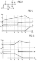
- Fig.s 4 and 5 show graphs of a number of electric quantities (not to scale) in the Fig.3 diagram as a function of standby voltage;
- Fig.6 shows a circuit diagram of the circuit according to the present invention.
- Fig.3 shows an
audio amplifier 1, and an on-off control circuit 15 comprisingcapacitor 6,resistor 7 andswitch 8, and in whichnode 16 common to bothcapacitor 6 andresistor 7 presents standby voltage VST supplied to the input ofaudio amplifier 1 over a line not shown.Circuit 15 also comprises six comparators 20-25. The negative inputs ofcomparators 20 and 24 and the positive inputs of comparators 21-23 are connected tonode 16; the positive inputs ofcomparators 20 and 24 and the negative inputs of comparators 21-23 are connected to respective reference voltages V₁, V₅, V₂, V₃, V₄; and the negative and positive inputs ofcomparator 25 are connected respectively to the negative input ofamplifier 1 and to reference voltage V₆. Voltages V₁-V₅ are so selected that V₁ < V₂ < V₃ < V₄ < V₅, whereas voltage V₆ is generated separately and independently of the others, and is lower than the steady-state value of voltage V+ at the positive input ofamplifier 1. -
Node 16 is also grounded via resistor 28, and connected to the supply via series connectedresistor 29 and switch 30. - The output of
comparator 20 is connected to a first input of anOR circuit 31, the second, inverted, input of which is connected to the output ofcomparator 23 viainverter 41; the output of comparator 21 is connected to the ON input ofamplifier 1; the output ofcomparator 22 is connected to the control terminal of aswitch 32 series connected to avoltage source 33 supplying voltage V₇, and located between the positive input ofamplifier 1 and ground; in addition toinverter 41, the output ofcomparator 23 is also connected to the control terminal of aswitch 37 series connected to aresistor 35 andcapacitor 36 between the positive and negative inputs ofamplifier 1; the output of comparator 24 is connected, viainverter 38, to the reset input of aramp generator 39, and directly to the control terminal of aswitch 40 between the output oframp generator 39 and the negative input ofamplifier 1; and the output ofcomparator 25 is connected to the control terminal of aswitch 42 betweennode 16 and ground. - The output of
OR circuit 31 is connected to the start input oframp generator 39, which is also connected tonode 16. When the start input is enabled,ramp generator 39 provides for generating an output voltage increasing from a minimum VMIN, equal to the instantaneous value of voltage V- at the negative input ofamplifier 1, to a maximum VMAX, equal to VST + 3Vbe (where Vbe is the typical base-emitter voltage drop of a normal transistor when on).Resistors amplifier 1 and ground. - With reference also to Fig. 4, off-on operation of
circuit 15 will now be described commencing from the full off condition wherein all the electric quantities are zeroed and supply voltage VCC is applied.

In this phase, the outputs ofcomparators 20 and 24 are high, so thatcomparator 20 supplies a start pulse toramp generator 39, comparator 24closes switch 40, and the voltage generated byramp generator 39 and increasing linearly from 0 V is applied to the negative input ofamplifier 1, thus increasing voltage V-. As long as V- remains lower than V₆, however, the output ofcomparator 25 remains high, so thatswitch 42 remains closed andnode 16 grounded.

When V-, increased by the ramp voltage, exceeds V₆, the output ofcomparator 25 switches to low, thus openingswitch 42 and enabling an increase in VST.

The output ofcomparator 20 simply switches to low.

The output of comparator 21 switches to high, thus turning onamplifier 1, the output of which however remains low by virtue of the higher potential at the negative as compared with the positive input.

Comparator 22 switches, thus closingswitch 32 and connectingvoltage source 33 to the positive input ofamplifier 1, which thus presents voltage V₇. As V₇, however, is lower than the voltage at the negative input (now equal to VMAX), the output ofamplifier 1 remains grounded.

The output ofcomparator 23 switches to high, so that switch 37 closes andcapacitor 36 begins charging. Due to the positive voltage remaining between the negative and positive inputs ofamplifier 1, however, the output of the amplifier remains low.

Comparator 24 switches so as to resetramp generator 39 and openswitch 40; the negative input ofamplifier 1, no longer forced to potential VMAX, tends towards potential V₇ at the positive input;capacitor 36 discharges the voltage at its terminals viaresistors switch 42 is kept open bycomparator 25, thus enabling the standby voltage to reach the steady-state value, and normal operation ofamplifier 1. - Operation as described above also applies when switching on from standby mode, by virtue of
switch 8, in standby mode, being closed and so maintaining a very low VST value of less than V₁. The only difference in this case is that, as opposed to zero, voltage V- at the negative input ofamplifier 1 presents a predetermined positive value, e.g. 3Vbe, so that, whenswitch 8 is opened, V- > V₆. Phase 1) is therefore skipped and operation commenced directly from phase 2). - Operation of the circuit will now be described relative to switching from normal operation to standby mode, for which purpose,
switch 8, which is normally open, is closed, andcapacitor 6 begins discharging so as to gradually reduce voltage VST.

In this phase, the outputs of comparators 21-23 are high, the outputs ofcomparators switches ramp generator 39 is reset; V- = V+ = V₇ and the output ofamplifier 1 operates normally.

Comparator 24 switches, thus closingswitch 40 and cancelling the reset signal to rampgenerator 39, which, in the absence of the start signal, however, remains idle.

Comparator 23 switches, thus openingswitch 37 and supplying the start signal to rampgenerator 39, which supplies an output voltage increasing gradually from VMIN (equal to V₇) to the negative input ofamplifier 1, so that V- becomes greater than V+, and Vo begins to fall.

Comparator 22 switches, thus openingswitch 32, and the positive input ofamplifier 1 is grounded, thus confirming V- > V+.

Comparator 21 switches, so as to turn off the internal sources ofamplifier 1 and consequently also the amplifier itself, the zero output of which, however, results in no undesired noise.

Comparator 20 switches, thus generating a start pulse forramp generator 39, which, in the absence of the reset signal, nevertheless remains idle. - The circuit therefore switches to standby mode wherein voltage VST presents a very low value, V+ = 0 V, and V- = VMAX = 3Vbe.
- For achieving the above timing, the Fig.3 voltages are preferably selected so that V₁ < 1 V; V₂ > 1.4 V; V₃ > 2.1 V; V₄ > 2.8 V; V₅ > 3.5 V; V₆ = 1 V; and V₇ = 1.4 V.
- The rise and fall time constant of the output is determined by the discharge and charge time constant of
capacitor 6. - Fig.6 shows one possible application of the Fig.3 configuration to a single-feed monophonic audio amplifier connected to a loudspeaker as shown in Fig.1. More specifically, Fig.6 shows
audio amplifier 1 with equivalentinternal resistance 50 between the output and negative input, andequivalent resistance 86 between the positive and negative inputs; components 6-8;feedback network loudspeaker 5. - The Fig.6 circuit comprises a
bias network 80 connected between the supply and anode 70 defined by the emitter of aPNP transistor 60 having its base connected to the negative input ofamplifier 1, and its collector grounded.Node 70 is connected to one terminal of a chain of twodiodes 61 and tworesistors resistors current source 74 and to the base of anNPN transistor 64, the emitter of which is grounded, and the collector of which is connected to a node between a resistor 65 (also connected to the supply) and acurrent mirror circuit 66 also connected to the standby input. Acurrent source 69 drives a differential stage comprising twoPNP transistors transistor 71 is connected to a node between a resistor 81 (also connected to the supply) and a series of seven diodes 72 (also grounded). The collector oftransistor 71 is grounded, and that oftransistor 53 connected to the negative input ofamplifier 1. The base oftransistor 53 is connected to the emitter of aPNP transistor 54, the collector of which is grounded, and the base of which is connected to a node between a resistor 67 (also connected to the supply) and the cathode of a diode 55, the anode of which is connected to the standby input and to a grounded chain comprising, in succession, aresistor 57 and a series of fourdiodes diodes NPN transistor 73, the emitter of which is grounded, and the collector of which controlssource 74. The same node is also connected to the base of an NPN transistor 85 (forming a current mirror withdiode 59 and transistor 73), the emitter of which is grounded, and the collector of which is connected to the negative input ofamplifier 1. The node betweenresistor 57 anddiodes 68 is connected to the control terminal of acurrent source 56 driving the internal sources ofamplifier 1. The positive input ofamplifier 1 is connected to the signal input terminal viacapacitor 82. - In the Fig.6 circuit,
comparator 20 is formed by components 53-55, 9 and 4; comparator 21 by components 56-59, 68;comparator 22,voltage source 33 and switch 32 bydiodes comparator 23 bycomponents transistor 60;comparator 25 by components 60-66;divider 29, 28 bycomponents ramp generator 39 by components 53-55, 9 and 4; and switch 42 bymirror circuit 66.Resistors internal resistance 86. - In the Fig.6 circuit, the steady-state direct current offset of output voltage Vo equals roughly half supply voltage VCC. In fact,
diode 59 is supplied with a predetermined current as a function of supply voltage, according to the equation:

where Vbe is the voltage drop ofdiodes resistors -
Transistor 85, forming a 1:1 mirror withdiode 59, conducts and supplies current I to resistor 50 also of value R. As the input stage ofamplifier 1 is formed by a differential amplifier and, for reasons of dynamics, the positive input is set to potential 2Vbe viadiodes


The steady-state standby potential equals

at which the current sources ofamplifier 1 are on; the amplifier is operative; and the audio signal at the IN input is transferred to the loudspeaker with a gain determined byfeedback network - When the circuit shown is switched from normal operation to standby mode, therefore, the output switches from VCC/2 to ground, and vice versa when the circuit is turned on, with a transient state controlled, according to the present invention, by applying a positive potential to the negative input in relation to the positive input, as described below.
- More specifically, when switched on from standby mode, the Fig.6 circuit operates as follows.
- In standby mode,
switch 8 is grounded by verylow resistor 7, so that the current sources of the amplifier are off; the current in the branch formed bycomponents transistors source 69 is high enough for the collector load oftransistor 53, this is saturated so that the collector connected to the negative input presents a potential of roughly 3Vbe. - To turn on the circuit,
switch 8 is opened, so as to chargecapacitor 6 slowly via fairlyhigh resistor 67. In this phase,transistor 60 is off, by virtue of its base presenting a potential of 3Vbe (potential V-) and its emitter the 3.5Vbe potential (of node 70) determined by the chain formed bydiodes 61, transistor 64 (on in this phase) andresistor 62, the terminals of which present a voltage of 0.5Vbe as divided betweenresistors transistor 64 is on,current mirror 66 is off, thus enabling charging of the standby voltage viacapacitor 6 andresistor 67. - As VST increases, the current sources of the amplifier are the first to be turned on (via
resistor 57 and current source 56); and upon VST reaching 2Vbe,diodes 68 are turned on and the positive input begins to rise. - Upon VST reaching 4Vbe,
diodes transistor 85 is turned on, thus absorbing the collector current oftransistor 53 and the current fromcapacitor 9; andcapacitor 9 begins discharging from the former 3Vbe + VST value. When VST reaches 5Vbe and the emitters oftransistors transistor 71 is turned on;differential stage source 69 is also supplied totransistor 71; and the current intransistor 53 falls, thus causing a further reduction in potential V- at the negative input. When VST > 5Vbe,transistor 53 is turned off, and the current fromsource 69 is supplied solely totransistor 71. In this phase,transistor 73, forming a current mirror withdiode 59, turns oncircuit 74, which in turn keepstransistor 64 on, so thatcurrent mirror circuit 66 remains definitely off, regardless of the potential at the base oftransistor 60. - The circuit is thus brought slowly up to the steady-state condition, but as long as V- > V+, output Vo of the amplifier remains grounded, despite the amplifier being turned on. Subsequently, as both the inputs of
amplifier 1 reach the same potential, thus balancing the amplifier, the output follows the standby voltage so as to switch to the steady-state value. - Operation of the circuit for switching from off to on is the same as described above, except that, in this case, voltage V- at the negative input of
amplifier 1 is initially zero, and is increased gradually by the charging ofcapacitor 9 bytransistor 53. In this phase, the potential at the base oftransistor 60 is low, so thattransistor 60 is turned on, thus lowering the voltage atnode 70; anddiodes 61 andtransistor 64 are off, so thatcurrent mirror 66 is on, thus maintaining a low potential at the standby input. This phase continues until V- exceeds 2.8Vbe, at which point,transistor 60 is turned off, andcomponent chain mirror 66 and so enabling an increase in voltage VST as described above. - Operation of the circuit will now be described relative to switching from normal operation to standby mode. When
switch 8 is closed,capacitor 6, charged to steady-state voltage
resistor 7. - As long as VST > 5Vbe,
transistor 53 is off, and the current fromsource 69 is supplied entirely totransistor 71. Subsequently,transistor 53 starts conducting to supplytransistor 85 andcapacitor 9. In this phase, the negative input does not increase immediately, but in controlled manner, by virtue oftransistor 85; while the output falls by following the potential at the standby input, to which it is related as a function of the (in this case, falling) collector current oftransistor 85. Whentransistor 85 is turned off,diode 59 is turned off due to the reduction in VST, so that the negative input increases more rapidly, while the potential at the positive input is zeroed, and the output ofamplifier 1 switches to 0 V due to unbalancing of the inputs. As the negative input increases further to 3Vbe, the amplifier sources, and consequently also the amplifier itself, remain on. When the sources are also turned off (VST ≃ 0 V), the amplifier is in standby mode. - It will be noted that the above sequences occur in the presence of supply voltage VCC, that is, in the presence of fixed references with the control circuits on.
- The advantages of the circuit according to the present invention will be clear from the foregoing description. In particular, it provides for controlled on or off switching at all times of the output, thus preventing transients resulting in undesired noise (popping).
- The function described may be employed when the user equipment is set to standby mode, for reducing line absorption, when turning off the volume or switching the signal source.
- The same circuit may also be employed for a single-ended two-channel audio amplifier operating in the same manner, by simply duplicating a number of structures, i.e. via the addition of a small number of components.
- The same pin on the audio amplifier integrating device may be employed for supply voltage rejection (SVR) or standby, i.e. for performing two functions; and a single capacitor (component 6) is capable of performing both the SVR function as well as determining the time constant of the on and off phases.
- The circuit also provides for an excellent compromise in terms of transition time and the noise produced in the loudspeakers.
- Finally, the circuit according to the present invention provides for a high degree of reliability, as well as troublefree manufacture and integration using current manufacturing techniques.
- To those skilled in the art it will be clear that changes may be made to the circuit as described and illustrated herein without, however, departing from the scope of the present invention.
Claims (9)
- A circuit (15) for on-off control of an audio amplifier (1) having a positive and negative input, and including current sources (56); characterized by the fact that it comprises voltage source means (20-24, 39, 40) for generating a controlled positive potential applicable to said negative input in relation to said positive input when said amplifier (1) is turned on or off.
- A circuit as claimed in Claim 1, characterized by the fact that said voltage source means comprise a first increasing voltage source (39) connectable to said inputs of said amplifier (1); first activating means (21) for generating a signal for turning on said current sources (56); first deactivating means (24) for deactivating said first voltage source (39); second activating means (20, VST) activated during the switch-on phase, for activating, in sequence, said first voltage source (39), said first activating means (21) and said first deactivating means (24); a second increasing voltage source (39) connectable to said inputs of said amplifier (1); second deactivating means (21) for deactivating said current sources (56); and third activating means (23, 24) activated during the switch-off phase, for activating, in sequence, said second voltage source (39) and said second deactivating means (21).
- A circuit as claimed in Claim 2, characterized by the fact that it also comprises a third voltage source (33) connectable to the positive input of said amplifier (1); and control means (22) activated by said second activating means (20, VST) subsequent to said first activating means (21), deactivated by said third activating means (23, 24) prior to said second deactivating means (21), and designed to activate said third voltage source (33).
- A circuit as claimed in Claim 3, characterized by the fact that said first (21), second (20) and third (23, 24) activating means, said first (24) and second (21) deactivating means, and said control means (22) consist of comparators.
- A circuit as claimed in any one of the foregoing Claims from 1 to 4, characterized by the fact that said first and second increasing voltage sources comprise a ramp generator (39).
- A circuit as claimed in any one of the foregoing Claims from 1 to 5 for an amplifier (1) having a standby input; characterized by the fact that it comprises a first (20), second (21), third (22), fourth (23), fifth (24) and sixth (25) comparator; said first (20) and fifth (24) comparators having a negative input connectable to said standby input, and said second (21), third (22) and fourth (23) comparators having a positive input connectable to said standby input; said first, second, third, fourth and fifth comparators having a second input connected to a respective gradually increasing reference voltage (V₁-V₅); said sixth comparator (25) having a negative input connectable to the negative input of said amplifier (1), and a positive input connected to a reference voltage (V₆); the output of said first comparator (20) driving a ramp generator (39) having its output connected to said negative input of said amplifier; the output of said second comparator (21) being connectable to a terminal enabling said current sources (56); the output of said third comparator (22) driving a first switch (32) between said positive input of said amplifier and a voltage source (33); the output of said fourth comparator (23) driving said ramp generator (39) and a second switch (37) on a line connecting said positive input to said negative input of said amplifier and including resistive means (35) and capacitive means (36); said fifth comparator (24) having its output connected to the reset input of said ramp generator (39) and to a third switch (40) between said output of said ramp generator (39) and said negative input of said amplifier (1); and said sixth comparator (25) having its output connected to a fourth switch (42) between said standby input and a reference potential line (ground).
- An amplifying circuit comprising an audio amplifier (1) and a circuit (15) for on-off control of said audio amplifier; said audio amplifier having a positive and a negative input, and including current sources (56); characterized by the fact that said on-off circuit (15) comprises voltage source means (20-24, 39, 40) for generating a controlled positive potential at said negative input in relation to said positive input when said amplifier (1) is switched on or off.
- An on-off method for an audio amplifier (1) having a positive input, a negative input, an output, and current sources (56); characterized by the fact that it comprises a phase wherein a controlled positive potential is generated at said negative input in relation to said positive input when said amplifier is turned on or off.
- A method as claimed in Claim 8, characterized by the fact that it comprises a turn-on phase and a turn-off phase; said turn-on phase comprising phases wherein a positive potential difference is generated between said negative input and said positive input of said amplifier, for maintaining said output at a reference potential; said current sources (56) are turned on, with said output at said reference potential; and said potential difference is reduced gradually for enabling said output to reach a steady-state value differing from said reference potential; said turn-off phase comprising phases wherein a positive potential difference is generated gradually between said negative input and said positive input of said amplifier, so as to bring said output gradually from said steady-state value to said reference potential, with said current sources (56) on, and turn off said current sources with said output at said reference potential.
Priority Applications (4)
| Application Number | Priority Date | Filing Date | Title |
|---|---|---|---|
| DE69231613T DE69231613T2 (en) | 1992-05-22 | 1992-05-22 | Control circuit for switching an audio amplifier on and off |
| EP92830254A EP0570655B1 (en) | 1992-05-22 | 1992-05-22 | Audio amplifier on-off control circuit |
| US08/065,633 US5363062A (en) | 1992-05-22 | 1993-05-21 | Audio amplifier on-off control circuit |
| JP5121547A JPH0637560A (en) | 1992-05-22 | 1993-05-24 | On-off control circuit and amplification circuit for audio amplifier and on-off method of audio amplifier |
Applications Claiming Priority (1)
| Application Number | Priority Date | Filing Date | Title |
|---|---|---|---|
| EP92830254A EP0570655B1 (en) | 1992-05-22 | 1992-05-22 | Audio amplifier on-off control circuit |
Publications (2)
| Publication Number | Publication Date |
|---|---|
| EP0570655A1 true EP0570655A1 (en) | 1993-11-24 |
| EP0570655B1 EP0570655B1 (en) | 2000-12-27 |
Family
ID=8212107
Family Applications (1)
| Application Number | Title | Priority Date | Filing Date |
|---|---|---|---|
| EP92830254A Expired - Lifetime EP0570655B1 (en) | 1992-05-22 | 1992-05-22 | Audio amplifier on-off control circuit |
Country Status (4)
| Country | Link |
|---|---|
| US (1) | US5363062A (en) |
| EP (1) | EP0570655B1 (en) |
| JP (1) | JPH0637560A (en) |
| DE (1) | DE69231613T2 (en) |
Cited By (5)
| Publication number | Priority date | Publication date | Assignee | Title |
|---|---|---|---|---|
| EP1071206A1 (en) * | 1999-07-20 | 2001-01-24 | STMicroelectronics S.r.l. | A receiver portion of a telephone |
| WO2002015388A2 (en) * | 2000-08-11 | 2002-02-21 | Maxim Integrated Products, Inc. | Amplifier circuits and methods to provide smooth transition of amplifier outputs during powering sequences |
| EP1899974A2 (en) * | 2005-06-29 | 2008-03-19 | Analog Devices, Inc. | Improved charge/discharge control circuit for audio device |
| WO2009099904A2 (en) * | 2008-01-31 | 2009-08-13 | Qualcomm Incorporated | System and method of reducing click and pop noise in audio playback devices |
| US8179192B2 (en) | 2007-03-07 | 2012-05-15 | Nxp B.V. | Signal processor comprising a reference voltage circuit |
Families Citing this family (17)
| Publication number | Priority date | Publication date | Assignee | Title |
|---|---|---|---|---|
| EP0678975B1 (en) * | 1994-04-15 | 1997-10-08 | STMicroelectronics S.r.l. | Low frequency amplifier |
| DE69413235T2 (en) | 1994-10-31 | 1999-01-28 | St Microelectronics Srl | Operational amplifier switchable in different configurations |
| US5648742A (en) * | 1995-10-23 | 1997-07-15 | National Semiconductor Corporation | Amplifier circuit with reduced turn-on and turn-off transients |
| US5642074A (en) * | 1995-10-13 | 1997-06-24 | National Semiconductor Corporation | Amplifier circuit with reduced turn-on and turn-off transients |
| US5939938A (en) * | 1995-10-13 | 1999-08-17 | National Semiconductor Corporation | Amplifier circuit with reduced DC power related turn-on and turn-off transients |
| US5703529A (en) * | 1995-10-13 | 1997-12-30 | National Semiconductor Corporation | Amplifier circuit with reduced DC power related transients |
| DE19547093A1 (en) * | 1995-12-16 | 1997-06-19 | Nokia Deutschland Gmbh | Circuit for improvement of noise immunity of audio signal |
| FR2853472B1 (en) * | 2003-04-01 | 2005-06-24 | St Microelectronics Sa | AUDIO AMPLIFIER CIRCUIT |
| US7283596B2 (en) * | 2003-07-08 | 2007-10-16 | Avago Technologies General Ip (Singapore) Pte Ltd | PAM-4 data slicer having symmetrical offset |
| TWI235543B (en) * | 2004-05-17 | 2005-07-01 | Analog And Power Electronics C | Amplifier circuit that prohibits instantaneous turn-on pop and method thereof |
| JP4535901B2 (en) * | 2005-02-16 | 2010-09-01 | 新日本無線株式会社 | Audio amplifier |
| JP4759015B2 (en) * | 2008-04-25 | 2011-08-31 | 株式会社リコー | Constant voltage circuit |
| WO2010111438A2 (en) | 2009-03-25 | 2010-09-30 | Pacid Technologies, Llc | System and method for protecting a secrets file |
| CN102324895B (en) * | 2011-07-01 | 2013-07-31 | 四川和芯微电子股份有限公司 | POP noise suppression circuit and method |
| US8779962B2 (en) * | 2012-04-10 | 2014-07-15 | Fairchild Semiconductor Corporation | Audio device switching with reduced pop and click |
| GB2560045B (en) * | 2017-02-28 | 2019-10-30 | Cirrus Logic Int Semiconductor Ltd | Amplifiers |
| CN116723451B (en) * | 2023-08-10 | 2023-11-03 | 上海海栎创科技股份有限公司 | Playback power supply control circuit and control method |
Citations (2)
| Publication number | Priority date | Publication date | Assignee | Title |
|---|---|---|---|---|
| EP0159079A2 (en) * | 1984-04-20 | 1985-10-23 | STMicroelectronics S.r.l. | Audio amplifier switch-on control circuit |
| EP0368528A2 (en) * | 1988-11-09 | 1990-05-16 | STMicroelectronics S.r.l. | Audio amplifier with mute and stand-by states |
-
1992
- 1992-05-22 EP EP92830254A patent/EP0570655B1/en not_active Expired - Lifetime
- 1992-05-22 DE DE69231613T patent/DE69231613T2/en not_active Expired - Fee Related
-
1993
- 1993-05-21 US US08/065,633 patent/US5363062A/en not_active Expired - Lifetime
- 1993-05-24 JP JP5121547A patent/JPH0637560A/en active Pending
Patent Citations (2)
| Publication number | Priority date | Publication date | Assignee | Title |
|---|---|---|---|---|
| EP0159079A2 (en) * | 1984-04-20 | 1985-10-23 | STMicroelectronics S.r.l. | Audio amplifier switch-on control circuit |
| EP0368528A2 (en) * | 1988-11-09 | 1990-05-16 | STMicroelectronics S.r.l. | Audio amplifier with mute and stand-by states |
Cited By (11)
| Publication number | Priority date | Publication date | Assignee | Title |
|---|---|---|---|---|
| EP1071206A1 (en) * | 1999-07-20 | 2001-01-24 | STMicroelectronics S.r.l. | A receiver portion of a telephone |
| US6535724B1 (en) | 1999-07-20 | 2003-03-18 | Stmicroelectronics S.R.L. | Receiver portion of a telephone |
| WO2002015388A2 (en) * | 2000-08-11 | 2002-02-21 | Maxim Integrated Products, Inc. | Amplifier circuits and methods to provide smooth transition of amplifier outputs during powering sequences |
| WO2002015388A3 (en) * | 2000-08-11 | 2003-08-21 | Maxim Integrated Products | Amplifier circuits and methods to provide smooth transition of amplifier outputs during powering sequences |
| EP1899974A2 (en) * | 2005-06-29 | 2008-03-19 | Analog Devices, Inc. | Improved charge/discharge control circuit for audio device |
| EP1899974A4 (en) * | 2005-06-29 | 2009-05-13 | Analog Devices Inc | Improved charge/discharge control circuit for audio device |
| US7991169B2 (en) | 2005-06-29 | 2011-08-02 | Analog Devices, Inc. | Charge/discharge control circuit for audio device |
| US8179192B2 (en) | 2007-03-07 | 2012-05-15 | Nxp B.V. | Signal processor comprising a reference voltage circuit |
| WO2009099904A2 (en) * | 2008-01-31 | 2009-08-13 | Qualcomm Incorporated | System and method of reducing click and pop noise in audio playback devices |
| WO2009099904A3 (en) * | 2008-01-31 | 2009-10-15 | Qualcomm Incorporated | System and method of reducing click and pop noise in audio playback devices |
| US9014396B2 (en) | 2008-01-31 | 2015-04-21 | Qualcomm Incorporated | System and method of reducing click and pop noise in audio playback devices |
Also Published As
| Publication number | Publication date |
|---|---|
| JPH0637560A (en) | 1994-02-10 |
| US5363062A (en) | 1994-11-08 |
| DE69231613D1 (en) | 2001-02-01 |
| EP0570655B1 (en) | 2000-12-27 |
| DE69231613T2 (en) | 2001-05-31 |
Similar Documents
| Publication | Publication Date | Title |
|---|---|---|
| EP0570655A1 (en) | Audio amplifier on-off control circuit | |
| US4983927A (en) | Integrated audio amplifier with combined regulation of the "mute" and "standby" functions and the switching transients | |
| US5939938A (en) | Amplifier circuit with reduced DC power related turn-on and turn-off transients | |
| US5796303A (en) | Popless amplifier | |
| US6445167B1 (en) | Linear regulator with a low series voltage drop | |
| EP1229639B1 (en) | Elimination of noise during power supply switching in an audio amplifier circuit | |
| US5436588A (en) | Click/pop free bias circuit | |
| US5307025A (en) | Audio power amplifier with noise prevention at turn-on and turn-off | |
| US7053704B2 (en) | Audio amplifier circuit with suppression of unwanted noise when starting from an off or standby state | |
| US6822884B1 (en) | Pulse width modulated charge pump | |
| US5220613A (en) | Audio amplifier circuit | |
| US7113031B2 (en) | Audio amplifier circuit with suppression of unwanted noise when powered on from standby | |
| JP2002330064A (en) | Boot strap circuit | |
| JP3323998B2 (en) | Power supply | |
| JPH08213849A (en) | Audio mute circuit | |
| WO2002015388A2 (en) | Amplifier circuits and methods to provide smooth transition of amplifier outputs during powering sequences | |
| JPH05198196A (en) | Method and apparatus for decreasing effect of sample-switch charge injection into plurality of series-connected sample-data comparators | |
| JPS6122345Y2 (en) | ||
| JPH03295472A (en) | Peak holding circuit | |
| JPH0955000A (en) | Generation circuit of recording and reproducing control signal and automatic control recording circuit | |
| JPH11163648A (en) | Sound muting circuit | |
| JPS61251302A (en) | Muting circuit | |
| KR920003804Y1 (en) | Simultaneous output circuit for high power amp | |
| JP2000194430A (en) | Power source circuit | |
| JPS58139193A (en) | Muting circuit for electronic musical instrument |
Legal Events
| Date | Code | Title | Description |
|---|---|---|---|
| PUAI | Public reference made under article 153(3) epc to a published international application that has entered the european phase |
Free format text: ORIGINAL CODE: 0009012 |
|
| AK | Designated contracting states |
Kind code of ref document: A1 Designated state(s): DE FR GB IT NL PT |
|
| 17P | Request for examination filed |
Effective date: 19940201 |
|
| 17Q | First examination report despatched |
Effective date: 19960311 |
|
| RAP3 | Party data changed (applicant data changed or rights of an application transferred) |
Owner name: STMICROELECTRONICS S.R.L. |
|
| GRAG | Despatch of communication of intention to grant |
Free format text: ORIGINAL CODE: EPIDOS AGRA |
|
| GRAG | Despatch of communication of intention to grant |
Free format text: ORIGINAL CODE: EPIDOS AGRA |
|
| GRAH | Despatch of communication of intention to grant a patent |
Free format text: ORIGINAL CODE: EPIDOS IGRA |
|
| GRAH | Despatch of communication of intention to grant a patent |
Free format text: ORIGINAL CODE: EPIDOS IGRA |
|
| GRAA | (expected) grant |
Free format text: ORIGINAL CODE: 0009210 |
|
| AK | Designated contracting states |
Kind code of ref document: B1 Designated state(s): DE FR GB IT NL PT |
|
| PG25 | Lapsed in a contracting state [announced via postgrant information from national office to epo] |
Ref country code: NL Free format text: LAPSE BECAUSE OF FAILURE TO SUBMIT A TRANSLATION OF THE DESCRIPTION OR TO PAY THE FEE WITHIN THE PRESCRIBED TIME-LIMIT Effective date: 20001227 |
|
| REF | Corresponds to: |
Ref document number: 69231613 Country of ref document: DE Date of ref document: 20010201 |
|
| ITF | It: translation for a ep patent filed |
Owner name: STUDIO TORTA S.R.L. |
|
| PG25 | Lapsed in a contracting state [announced via postgrant information from national office to epo] |
Ref country code: PT Free format text: LAPSE BECAUSE OF FAILURE TO SUBMIT A TRANSLATION OF THE DESCRIPTION OR TO PAY THE FEE WITHIN THE PRESCRIBED TIME-LIMIT Effective date: 20010327 |
|
| ET | Fr: translation filed | ||
| NLV1 | Nl: lapsed or annulled due to failure to fulfill the requirements of art. 29p and 29m of the patents act | ||
| PLBE | No opposition filed within time limit |
Free format text: ORIGINAL CODE: 0009261 |
|
| STAA | Information on the status of an ep patent application or granted ep patent |
Free format text: STATUS: NO OPPOSITION FILED WITHIN TIME LIMIT |
|
| 26N | No opposition filed | ||
| REG | Reference to a national code |
Ref country code: GB Ref legal event code: IF02 |
|
| PGFP | Annual fee paid to national office [announced via postgrant information from national office to epo] |
Ref country code: DE Payment date: 20020529 Year of fee payment: 11 |
|
| PG25 | Lapsed in a contracting state [announced via postgrant information from national office to epo] |
Ref country code: DE Free format text: LAPSE BECAUSE OF NON-PAYMENT OF DUE FEES Effective date: 20031202 |
|
| PGFP | Annual fee paid to national office [announced via postgrant information from national office to epo] |
Ref country code: FR Payment date: 20040510 Year of fee payment: 13 |
|
| PGFP | Annual fee paid to national office [announced via postgrant information from national office to epo] |
Ref country code: GB Payment date: 20040519 Year of fee payment: 13 |
|
| PG25 | Lapsed in a contracting state [announced via postgrant information from national office to epo] |
Ref country code: IT Free format text: LAPSE BECAUSE OF NON-PAYMENT OF DUE FEES;WARNING: LAPSES OF ITALIAN PATENTS WITH EFFECTIVE DATE BEFORE 2007 MAY HAVE OCCURRED AT ANY TIME BEFORE 2007. THE CORRECT EFFECTIVE DATE MAY BE DIFFERENT FROM THE ONE RECORDED. Effective date: 20050522 Ref country code: GB Free format text: LAPSE BECAUSE OF NON-PAYMENT OF DUE FEES Effective date: 20050522 |
|
| GBPC | Gb: european patent ceased through non-payment of renewal fee |
Effective date: 20050522 |
|
| PG25 | Lapsed in a contracting state [announced via postgrant information from national office to epo] |
Ref country code: FR Free format text: LAPSE BECAUSE OF NON-PAYMENT OF DUE FEES Effective date: 20060131 |
|
| REG | Reference to a national code |
Ref country code: FR Ref legal event code: ST Effective date: 20060131 |