EP0519649A2 - Single stage power factor corrected converter having isolated output - Google Patents
Single stage power factor corrected converter having isolated output Download PDFInfo
- Publication number
- EP0519649A2 EP0519649A2 EP92305366A EP92305366A EP0519649A2 EP 0519649 A2 EP0519649 A2 EP 0519649A2 EP 92305366 A EP92305366 A EP 92305366A EP 92305366 A EP92305366 A EP 92305366A EP 0519649 A2 EP0519649 A2 EP 0519649A2
- Authority
- EP
- European Patent Office
- Prior art keywords
- voltage
- power
- capacitor
- energy
- power converter
- Prior art date
- Legal status (The legal status is an assumption and is not a legal conclusion. Google has not performed a legal analysis and makes no representation as to the accuracy of the status listed.)
- Granted
Links
Images


Classifications
-
- H—ELECTRICITY
- H02—GENERATION; CONVERSION OR DISTRIBUTION OF ELECTRIC POWER
- H02M—APPARATUS FOR CONVERSION BETWEEN AC AND AC, BETWEEN AC AND DC, OR BETWEEN DC AND DC, AND FOR USE WITH MAINS OR SIMILAR POWER SUPPLY SYSTEMS; CONVERSION OF DC OR AC INPUT POWER INTO SURGE OUTPUT POWER; CONTROL OR REGULATION THEREOF
- H02M1/00—Details of apparatus for conversion
- H02M1/42—Circuits or arrangements for compensating for or adjusting power factor in converters or inverters
- H02M1/4208—Arrangements for improving power factor of AC input
- H02M1/4241—Arrangements for improving power factor of AC input using a resonant converter
-
- H—ELECTRICITY
- H02—GENERATION; CONVERSION OR DISTRIBUTION OF ELECTRIC POWER
- H02M—APPARATUS FOR CONVERSION BETWEEN AC AND AC, BETWEEN AC AND DC, OR BETWEEN DC AND DC, AND FOR USE WITH MAINS OR SIMILAR POWER SUPPLY SYSTEMS; CONVERSION OF DC OR AC INPUT POWER INTO SURGE OUTPUT POWER; CONTROL OR REGULATION THEREOF
- H02M3/00—Conversion of dc power input into dc power output
- H02M3/22—Conversion of dc power input into dc power output with intermediate conversion into ac
- H02M3/24—Conversion of dc power input into dc power output with intermediate conversion into ac by static converters
- H02M3/28—Conversion of dc power input into dc power output with intermediate conversion into ac by static converters using discharge tubes with control electrode or semiconductor devices with control electrode to produce the intermediate ac
- H02M3/325—Conversion of dc power input into dc power output with intermediate conversion into ac by static converters using discharge tubes with control electrode or semiconductor devices with control electrode to produce the intermediate ac using devices of a triode or a transistor type requiring continuous application of a control signal
- H02M3/335—Conversion of dc power input into dc power output with intermediate conversion into ac by static converters using discharge tubes with control electrode or semiconductor devices with control electrode to produce the intermediate ac using devices of a triode or a transistor type requiring continuous application of a control signal using semiconductor devices only
-
- H—ELECTRICITY
- H02—GENERATION; CONVERSION OR DISTRIBUTION OF ELECTRIC POWER
- H02M—APPARATUS FOR CONVERSION BETWEEN AC AND AC, BETWEEN AC AND DC, OR BETWEEN DC AND DC, AND FOR USE WITH MAINS OR SIMILAR POWER SUPPLY SYSTEMS; CONVERSION OF DC OR AC INPUT POWER INTO SURGE OUTPUT POWER; CONTROL OR REGULATION THEREOF
- H02M1/00—Details of apparatus for conversion
- H02M1/42—Circuits or arrangements for compensating for or adjusting power factor in converters or inverters
- H02M1/4208—Arrangements for improving power factor of AC input
- H02M1/4258—Arrangements for improving power factor of AC input using a single converter stage both for correction of AC input power factor and generation of a regulated and galvanically isolated DC output voltage
-
- Y—GENERAL TAGGING OF NEW TECHNOLOGICAL DEVELOPMENTS; GENERAL TAGGING OF CROSS-SECTIONAL TECHNOLOGIES SPANNING OVER SEVERAL SECTIONS OF THE IPC; TECHNICAL SUBJECTS COVERED BY FORMER USPC CROSS-REFERENCE ART COLLECTIONS [XRACs] AND DIGESTS
- Y02—TECHNOLOGIES OR APPLICATIONS FOR MITIGATION OR ADAPTATION AGAINST CLIMATE CHANGE
- Y02B—CLIMATE CHANGE MITIGATION TECHNOLOGIES RELATED TO BUILDINGS, e.g. HOUSING, HOUSE APPLIANCES OR RELATED END-USER APPLICATIONS
- Y02B70/00—Technologies for an efficient end-user side electric power management and consumption
- Y02B70/10—Technologies improving the efficiency by using switched-mode power supplies [SMPS], i.e. efficient power electronics conversion e.g. power factor correction or reduction of losses in power supplies or efficient standby modes
Landscapes
- Engineering & Computer Science (AREA)
- Power Engineering (AREA)
- Dc-Dc Converters (AREA)
- Rectifiers (AREA)
- Circuit Arrangements For Discharge Lamps (AREA)
- Ac-Ac Conversion (AREA)
Abstract
Description
- This invention relates to switching power converters and, in particular, to switching power converters having an input rectifier connected to an AC line source of energy and to arrangements to limit the generation of harmonics at the AC input.
- Switching power converters powered directly off of an AC power line are commonly designated as off line switchers (OLS). These converters rectify the AC voltage of the line and store it as a unipolar voltage on a voltage storage capacitor. This unipolar voltage, stored on the voltage storage capacitor, is applied to subsequent power switching circuitry for DC to DC power processing.
- The input impedance characteristics of an OLS are largely defined by its input rectifier and voltage storage capacitor. The voltage retention and the current sink characteristics of the voltage storage capacitor combine to make the line current conduction time of the rectifiers to be highly peaked and much shorter in duration than the half cycle duration of the input AC voltage waveform. Since the current waveforms are distorted from the desired sinusoidal waveforms the actual current waveforms induce a high harmonic content in the input current. These harmonic signals are returned to the input line and cause EMI problems to the supply network. The power factor at the input is significantly degraded, since the real power is extracted only from the waveform portion of the input current which is in phase with the applied voltage waveform.
- Filters are often used at the input of the power converter to block the application of harmonics to the AC line. The filter is normally tuned to eliminate the third and fifth harmonics. Many other harmonicas are generated however and hence, passive filters are limited in their ability to achieve very high power factors. Boost converters have also been used as an active filter input stage to reduce the harmonics at the AC input line where improved performance is required. The boost converter switch is modulated so that the line current waveform is maintained essentially at the fundamental frequency of the applied AC input voltage. A power conversion stage usually follows the boost converter and is needed to provide line isolation and regulation of the DC output signal. Thus, often two cascaded converters are required to achieve low harmonics at the input and achieve input output isolation between the AC input and the DC output.
- A particular power converter operative off of an AC power line to achieve high power factors and provide isolation between input and output is disclosed in assignees co-pending patent application serial number 07/59410 filed 09/28/91 and entitled "Single Conversion Power Factor Correction Using SEPIC Converter" This converter achieves high power factors, and hence, the current inertia characteristics of its energy storage inductor place large voltage stresses on the converter power switches.
- A power converter (OLS) is operative to reduce harmonics at its AC line input by controlling its power switching so that a current waveform in a switched inductor is maintained substantially identical to a waveform of a rectified version of the input AC voltage waveform. In one preferred embodiment of the invention, the voltage spikes induced by the switching of the inductor into a power train circuit that includes the leakage inductance of the power transformer are subdued by circuitry that absorbs the initial voltage spike temporarily and then delivers that energy to the output load of the power converter.
- In the Drawing:
- FIG. 1 is a schematic of a power train of a OLS embodying the principles of the invention; and
- FIG. 2 is a schematic of the OLS of FIG. 1 including the control circuitry controlling operation of the circuitry.
- FIGS. 3 and 4 show alternative arrangements of the power input circuitry for the power circuitry of FIGS. 2 and 3.
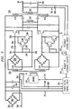
- The power train schematic of a power converter (OLS) powered off of an AC line voltage source and having power factor correction capabilities in accord with the principles of the invention is disclosed in FIG. 1. The
input terminals 101 and 102 are connected to an AC power line such as is provided by a commercial energy utility.Terminals 101 and 102 are connected to a full-wave rectifier 103 comprising the rectifyingdiodes full wave rectifier pass filter capacitor 110. Highpass filter capacitor 110 is selected to present a low impedance to the high frequency signals due to the switching of the converter's power switches and present a high impedance to signals at the AC power line frequency. - The high
pass filter capacitor 110 is connected by thesteering diode 111 to a power switching circuit comprisingFET power switches transient sink capacitor 112. Capacitor 112 has a charge acceptance capacity sufficient to sink anticipated transient spike energy due to converter power switching action. This spike energy is induced by distributed circuit loop inductances of the converter and by the power transformer leakage inductances. - A
circuit node 113 common to thediode 111 andcapacitor 112 is connected to acircuit node 114 of theFET switch 115 and the firstprimary winding 118 of thepower transformer 120.Lead 109 serves as a ground return from a secondprimary winding 119 of thepower transformer 120. - An
energy storage inductor 130 is connected between thecircuit nodes Circuit node 131 is common to theFET switch 115 and to aDC blocking capacitor 133,coupling node 131 to the firstprimary winding 118.Circuit node 132 is common to theFET switch 117 and to aDC blocking capacitor 134coupling node 132 to the secondprimary winding 119. - A
secondary winding 121 oftransformer 120 is coupled, viadiode 135, to acapacitor 136 which provides energy storage to smooth the output voltage supplied by theoutput terminals - In operation the input AC voltage at
terminals 101 and 102 is rectified by the full-wave rectifier 103. This rectified voltage is a unipolar half cycle sinusoid waveform voltage and as such is imposed on thecapacitor 110. The voltage waveform across thecapacitor 110 is a half sinusoid waveform with the half cycle waveform substantially identical to the half cycle waveform of the input voltage waveform. - The voltage on
capacitor 110 is coupled by adiode 111 to theFET power switches energy storage inductor 130, connected in series with the twoswitches voltage storage capacitor 110. A voltagetransient sink capacitor 112 shunts the the series connection of the twoswitches inductor 130 and is operative to reduce switching stress onswitches - Both the
FET switches capacitor 110 is applied to theinductor 130 and electrical energy is stored therein. The charging current flow through theinductor 130 causes a voltage drop therein with thenode 131 being positive with respect to thenode 132. During the subsequent non-conduction of the twoswitches inductor 130 is applied to the twoprimary windings power transformer 120.Node 131 is coupled to theprimary winding 118, via theDC blocking capacitor 133, andnode 132 is coupled to theprimary winding 119, via thedc blocking capacitor 134. Due to the current inertia characteristics of theinductor 130 the voltage atnode 131 is now negative with respect to thenode 132. Hence, current flow in thewindings secondary winding 121 is also positive at its polarity dot and hence, this voltage forward biases thediode 135 and the voltage of thewinding 121 is applied to theoutput terminals - The
transformer 120 includes a substantial amount of leakage inductance and when theinductor 130 is connected to thewindings inductor 130 to thewindings FET power switches - Two circuit paths, each including a steering diode (
diode voltage sink capacitor 112, respectively. The firstpath including diode 144 connects thenode 132 tonode 113.Diode 145 of the second path connectsnode 116 to thenode 131. Node 116 is in turn connected tolead 109 which is connected to the grounded plate of thesink capacitor 112. When the two FET switches 115 and 117 are biased into a non-conducting state, the inductor immediately reverses its voltage polarity as it attempts to maintain its current flow.Node 132 is at this instant positive with respect to thenode 131. Due to the leakage inductance of the primary windings oftransformer 120 the current ofinductor 130 can not immediately flow in a path including theprimary windings Diode 144 is forward biased by the positive voltage of thenode 132. The positive current output of theinductor 130 atnode 132 is transmitted by thediode 144 to the transientvoltage sink capacitor 112. The voltage ofnode 131 is now negative with respect to the ground voltage ofnode 116 thereby forward biasing thediode 145, and hence, a current flow is enabled from thenode 116 tonode 131. Thus, the immediate inertia current output of theinductor 130 is absorbed through thediodes voltage sink capacitor 112. Hence, the voltage stress across the FET switches 115 and 117 is significantly reduced. This current flow is of momentary duration until the current begins to flow through theprimary windings - A schematic of the power converter including the regulation and control circuitry is shown in FIG. 2. The AC line power is applied to the
input terminals full wave rectifier 203. The rectified voltage is stored on thevoltage storage capacitor 210 and is periodically coupled to theenergy storage inductor 230 by the conducting FET power switches 215 and 217, as described above with respect to the circuit of FIG.1. The energy stored in theenergy storage inductor 230 is delivered to the first and secondprimary windings transformer 220 while the FET power switches 215 and 217 are non-conducting. Output power is derived from the secondary winding 221 and coupled to a load byoutput terminals 241 and 242. - Feedback circuitry monitors the output voltage and power factor control circuitry monitors the voltage and current waveforms of the unipolar voltage output of the full-
wave rectifier 203. The waveform of the voltage stored on the voltage storage capacitor is monitored, via asensing lead 251 connected to the output of therectifier 203. Two sensing leads 258 and 259 are connected to sense a voltage due to current flow in aresistor 262 in the return lead connected to the full-wave rectifier 203. These sensing leads are all connected to a powerfactor control circuit 255 which responds to the above sensed signals and an error signal supplied from the converter secondary to generate a pulse width modulated drive signal for the power switches that optimizes power factor at the input by controlling a current waveform ininductor 230 and additionally regulates the output voltage. A suitable unit for thepower factor controller 255 is the commercially available integrated circuit designated as the UC1854 which is available from Unitrode. - The output voltage of the power converter is sensed, via the sensing leads 261 and 262. This sensed output voltage is connected to the
secondary control circuit 263. Here it is compared with a reference voltage and an error voltage proportional to a deviation of the output voltage from a desired regulated value is generated. This error voltage is coupled, vialead 266, to the primary tosecondary isolator 267, which couples it to the powerfactor control circuit 255. Theisolator 267 may comprise a signal transformer, an opto-isolator or some other suitable equivalent device. - The
power factor controller 255 multiplies the sensed rectifier input voltage onlead 251, derived from the input line voltage, with the error voltage derived from the output voltage and compares it to the voltage across leads 258 and 259 of the line current through theresistor 262. The resultant output of the power factor controller is a form of modulated drive pulses at a frequency greatly in excess of the AC line frequency. These drive pulses determine the switching frequency and duty cycle of the two FET power switches 215 and 217. - These modulated pulses supplied by the power
factor control circuit 255 are applied, vialead 271, to adriver circuit 272. The output of thedriver circuit 272 is a bipolar modulated drive pulse, whose pulse duration is modulated in response to the power factor control circuit 252. It is connected to the primary winding 273 of thedrive transformer 275.Transformer 275 includes twosecondary windings FET switch devices - The bias circuits for
FET switch switch 215 is discussed. The bipolar pulse output of the secondary winding 276 is rectified by the full-wave rectifier 278 producing a unipolar drive pulse having a pulse voltage such thatnode 291 is positive with respect tonode 292. This rectified pulse signal is coupled via thediode 279 andresistor 280 to thenode 293 common to the gate electrode of theFET switch 215 and to the emitter oftransistor 283 and the collector oftransistor 284. As long as thenode 291 is positive with respect tonode 292, the twotransistors node 291 fails in voltage with respect to the voltage ofnode 292 and thetransistors transistors FET 215 forcing it to turn off. - Different variations of the input circuitry of the converter are shown in the FIGS. 3, and 4 In the variation of FIG. 3 the high
pass filter capacitor 310 is connected across the input leads 301 and 302. No added dioded is necessary to separate thecapacitor resistor 491 andcapacitor 492 is connected across theenergy storage inductor 430. This particular variation permits the elimination of the twodiodes transient sink capacitor 112 shown in FIG. 1. - While a particular illustrative embodiment of the invention has been disclosed herein many variations may be devised by those skilled in the art without departing from the spirit and scope of the invention.
Claims (5)
- A power converter adapted to be energized by an AC line voltage source;
comprising:
means for accepting the AC line voltage and supplying a unipolar voltage derived from the AC line voltage;
a voltage transient sink capacitor connected to be charged by an output of the means for supplying;
a voltage storage capacitor coupled to the voltage transient sink capacitor by an isolating diode;
an output circuit for coupling energy to a load and including a transformer having first and second primary windings each having an inductive impedance at its energy receiving input;
an energy storage inductance;
CHARACTERIZED BY:
first and second power switches connected to opposite terminals of the inductor, and each connected substantially in parallel with the first and second primary windings respectively and operative when in a conducting mode to complete a continuous current path including the voltage storage capacitor and the energy storage inductance;
first and second unidirectional conduction paths operative when the first and second power switches are in a non-conducting mode to connect the energy storage inductance to the voltage transient sink capacitor. A power converter adapted to be energized by an AC line voltage source; - A power converter adapted to be energized by an AC line voltage source as claimed in claim 1;
CHARACTERIZED BY:
a switching circuitry control for forming alternate switching circuitry connections operative for alternately connecting the power converter in the conducting mode and the non-conducting mode of operation, in which the conduction mode is enabled by simultaneous conduction of the first and second power switches to enable energy flow from the voltage transient sink capacitor to the energy storage inductance while disconnecting the energy storage inductance from the power transformer and in which a the non-conducting mode is enabled by simultaneous non-conduction of the first and second power switches to enable a flow of energy stored in the energy storage inductance to the first and second primary windings of the power transformer. - A power converter adapted to be energized by an AC line voltage source as claimed in claim 2;
CHARACTERIZED BY:
the switching control circuitry including switch drive circuitry for driving the first and second power switches with a modulation scheme to control a current wave form of current in the energy storage inductor to have a waveform that enhances a power factor at the means for accepting. - A power converter adapted to be energized by an AC line voltage source as claimed in claim 3;
CHARACTERIZED BY:
unidirectional current conduction path enabled during the non-conduction mode for coupling initial voltage transients caused by the non-conduction mode to the the voltage transient sink capacitor. - A power converter adapted to be energized by an AC line voltage source as claimed in claim 4;
CHARACTERIZED BY:
the voltage transient sink capacitor having charge storage capacity sufficient for absorbing voltage spike energy and insufficient charge storage capacity for operably storing a sufficient charge to equal a voltage of the voltage storage capacitor.
Applications Claiming Priority (2)
| Application Number | Priority Date | Filing Date | Title |
|---|---|---|---|
| US07/716,464 US5146396A (en) | 1991-06-17 | 1991-06-17 | Single stage power factor corrected converter having isolated output |
| US716464 | 1991-06-17 |
Publications (3)
| Publication Number | Publication Date |
|---|---|
| EP0519649A2 true EP0519649A2 (en) | 1992-12-23 |
| EP0519649A3 EP0519649A3 (en) | 1993-01-27 |
| EP0519649B1 EP0519649B1 (en) | 1995-12-20 |
Family
ID=24878088
Family Applications (1)
| Application Number | Title | Priority Date | Filing Date |
|---|---|---|---|
| EP92305366A Expired - Lifetime EP0519649B1 (en) | 1991-06-17 | 1992-06-11 | Single stage power factor corrected converter having isolated output |
Country Status (9)
| Country | Link |
|---|---|
| US (1) | US5146396A (en) |
| EP (1) | EP0519649B1 (en) |
| KR (1) | KR930001554A (en) |
| DE (1) | DE69206894T2 (en) |
| ES (1) | ES2081568T3 (en) |
| FI (1) | FI922774A (en) |
| HK (1) | HK119396A (en) |
| NO (1) | NO922328L (en) |
| TW (1) | TW214021B (en) |
Cited By (1)
| Publication number | Priority date | Publication date | Assignee | Title |
|---|---|---|---|---|
| EP0928059A2 (en) * | 1998-01-05 | 1999-07-07 | Reinhard Kalfhaus | Current-voltage converter and relative control circuit |
Families Citing this family (13)
| Publication number | Priority date | Publication date | Assignee | Title |
|---|---|---|---|---|
| KR0115015Y1 (en) * | 1991-09-19 | 1998-10-01 | 이헌조 | Switching driving circuit |
| DE4135568A1 (en) * | 1991-10-29 | 1993-05-06 | Abb Patent Gmbh, 6800 Mannheim, De | SWITCH-OFF RELIEF NETWORK FOR POWER TRANSISTORS IN MULTI-TRANSISTOR CONVERTER |
| US5587892A (en) * | 1994-10-04 | 1996-12-24 | Delco Electronics Corp. | Multi-phase power converter with harmonic neutralization |
| JPH08168249A (en) * | 1994-10-11 | 1996-06-25 | Sony Corp | Current resonance switching power source circuit |
| US5610451A (en) * | 1995-11-30 | 1997-03-11 | Magnum Power Plc | Uninterruptible power supply with power factor correction |
| US5731969A (en) * | 1996-07-29 | 1998-03-24 | Small; Kenneth T. | Three-phase AC power converter with power factor correction |
| US5923152A (en) * | 1997-02-20 | 1999-07-13 | Astec International Limited | Power factor correction circuit with soft switched boost converter |
| US5790395A (en) * | 1997-02-27 | 1998-08-04 | Hagen; Thomas E. | Low in-rush current power factor control circuit |
| US5874809A (en) * | 1997-02-27 | 1999-02-23 | Hagen; Thomas E. | Constant light output ballast circuit |
| US6104172A (en) * | 1997-07-01 | 2000-08-15 | Power-One | Power factor corrector |
| US7034604B2 (en) * | 2003-03-17 | 2006-04-25 | Schweitzer Engineering Laboratories, Inc. | Communications device powered from host apparatus |
| US6853564B2 (en) * | 2003-03-25 | 2005-02-08 | Switching Power, Inc. | Switched linear inductor circuit for switched power supply |
| AT504961B1 (en) * | 2006-12-19 | 2010-01-15 | Siemens Ag Oesterreich | CIRCUIT ARRANGEMENT FOR REDUCED SWITCH LOAD |
Citations (1)
| Publication number | Priority date | Publication date | Assignee | Title |
|---|---|---|---|---|
| DE3004000B1 (en) * | 1980-02-04 | 1981-08-20 | Siemens AG, 1000 Berlin und 8000 München | Clocked power supply |
Family Cites Families (12)
| Publication number | Priority date | Publication date | Assignee | Title |
|---|---|---|---|---|
| US4184197A (en) * | 1977-09-28 | 1980-01-15 | California Institute Of Technology | DC-to-DC switching converter |
| US4384321A (en) * | 1980-04-29 | 1983-05-17 | California Institute Of Technology | Unity power factor switching regulator |
| US4403269A (en) * | 1982-03-05 | 1983-09-06 | International Business Machines Corporation | Non-dissipative snubber circuit apparatus |
| JPS58215970A (en) * | 1982-06-10 | 1983-12-15 | Fujitsu Ltd | Switching power source |
| US4618919A (en) * | 1984-10-04 | 1986-10-21 | Sperry Corporation | Topology for miniature power supply with low voltage and low ripple requirements |
| US4594649A (en) * | 1985-03-01 | 1986-06-10 | Ncr Corporation | Bootstrap drive for a two-transistor forward converter |
| JPS62163568A (en) * | 1986-01-14 | 1987-07-20 | Kikusui Denshi Kogyo Kk | Switching power source circuit |
| US4868730A (en) * | 1986-07-15 | 1989-09-19 | Combustion Electromagnetics, Inc. | DC to DC converter current pump |
| US4754385A (en) * | 1987-01-30 | 1988-06-28 | Varo, Inc. | Two transistor flyback switching converter with current sensing for discontinuous operation |
| DE3724649A1 (en) * | 1987-07-25 | 1989-02-02 | Leybold Ag | DEVICE FOR A UNIPOLAR OPERATED, ENERGY STORAGE COMPONENT |
| FR2634957B1 (en) * | 1988-07-29 | 1993-03-26 | Thomson Csf | CONTINUOUS / CONTINUOUS VOLTAGE CONVERTER TYPE CUK, AND DIRECT CONVERSION POWER SUPPLY MADE FROM SUCH A CONVERTER |
| US4870553A (en) * | 1988-11-04 | 1989-09-26 | Compaq Computer Corporation | Double-switched flyback power-converter |
-
1991
- 1991-06-17 US US07/716,464 patent/US5146396A/en not_active Expired - Fee Related
-
1992
- 1992-06-11 DE DE69206894T patent/DE69206894T2/en not_active Expired - Fee Related
- 1992-06-11 EP EP92305366A patent/EP0519649B1/en not_active Expired - Lifetime
- 1992-06-11 ES ES92305366T patent/ES2081568T3/en not_active Expired - Lifetime
- 1992-06-11 KR KR1019920010108A patent/KR930001554A/en not_active Application Discontinuation
- 1992-06-12 NO NO92922328A patent/NO922328L/en unknown
- 1992-06-16 FI FI922774A patent/FI922774A/en not_active Application Discontinuation
- 1992-06-18 TW TW081104771A patent/TW214021B/zh active
-
1996
- 1996-07-04 HK HK119396A patent/HK119396A/en not_active IP Right Cessation
Patent Citations (1)
| Publication number | Priority date | Publication date | Assignee | Title |
|---|---|---|---|---|
| DE3004000B1 (en) * | 1980-02-04 | 1981-08-20 | Siemens AG, 1000 Berlin und 8000 München | Clocked power supply |
Non-Patent Citations (1)
| Title |
|---|
| INTELEC '89 CONF. PROCEEDINGS October 1989, FLORENCE, ITALY pages 11.4 1 - 5 , XP000130007 PICCIRILLO & OCCHIENA 'Off-Line Switching Rectifier for Energy Plant' * |
Cited By (4)
| Publication number | Priority date | Publication date | Assignee | Title |
|---|---|---|---|---|
| EP0928059A2 (en) * | 1998-01-05 | 1999-07-07 | Reinhard Kalfhaus | Current-voltage converter and relative control circuit |
| DE19800105A1 (en) * | 1998-01-05 | 1999-07-15 | Reinhard Kalfhaus | Current-voltage converter and associated control loop |
| US6094366A (en) * | 1998-01-05 | 2000-07-25 | Kalfhaus; Reinhard | Current-to-voltage converter and associate closed-loop control circuit |
| EP0928059A3 (en) * | 1998-01-05 | 2002-03-13 | Reinhard Kalfhaus | Current-voltage converter and relative control circuit |
Also Published As
| Publication number | Publication date |
|---|---|
| TW214021B (en) | 1993-10-01 |
| FI922774A (en) | 1992-12-18 |
| HK119396A (en) | 1996-07-12 |
| DE69206894D1 (en) | 1996-02-01 |
| EP0519649A3 (en) | 1993-01-27 |
| NO922328D0 (en) | 1992-06-12 |
| NO922328L (en) | 1992-12-18 |
| KR930001554A (en) | 1993-01-16 |
| US5146396A (en) | 1992-09-08 |
| DE69206894T2 (en) | 1996-05-23 |
| EP0519649B1 (en) | 1995-12-20 |
| ES2081568T3 (en) | 1996-03-16 |
| FI922774A0 (en) | 1992-06-16 |
Similar Documents
| Publication | Publication Date | Title |
|---|---|---|
| USRE37889E1 (en) | Low loss synchronous rectifier for application to clamped-mode power converters | |
| US5781419A (en) | Soft switching DC-to-DC converter with coupled inductors | |
| US6906930B2 (en) | Structure and method for an isolated boost converter | |
| US4814962A (en) | Zero voltage switching half bridge resonant converter | |
| US5625541A (en) | Low loss synchronous rectifier for application to clamped-mode power converters | |
| US4493017A (en) | Single drive transformer with regenerative winding for p.w.m. supply having alternately conducting power devices | |
| EP0658968B1 (en) | Switching regulator | |
| EP0519649B1 (en) | Single stage power factor corrected converter having isolated output | |
| EP0503862B1 (en) | Class E fixed frequency converter | |
| EP0479453A2 (en) | Single conversion power factor correction using sepic converter | |
| WO2003052913A1 (en) | Flyback power converter | |
| US6256209B1 (en) | AC to DC conversion arrangement | |
| US7002323B2 (en) | Switching power supply circuit capable of reducing switching loss and control method used therein | |
| CA2311584A1 (en) | Frequency converter and ups employing the same | |
| US4821165A (en) | High voltage DC power supply | |
| US6137697A (en) | Universal switched power converter with demagnetising | |
| EP1034597B1 (en) | Charge circuits for ups | |
| US5036450A (en) | Spike limiting circuit | |
| US4945464A (en) | High voltage DC power supply | |
| JP3235711B2 (en) | Switching power supply | |
| EP0763277A1 (en) | Circuit arrangement | |
| JPH053672A (en) | Spike absorbing circuit for power supply circuit | |
| JPH1066335A (en) | Converter circuit | |
| JPH05236748A (en) | Power source unit | |
| EP1252701A2 (en) | Multi-output switched power converter providing an uninterrupted voltage at one output |
Legal Events
| Date | Code | Title | Description |
|---|---|---|---|
| PUAI | Public reference made under article 153(3) epc to a published international application that has entered the european phase |
Free format text: ORIGINAL CODE: 0009012 |
|
| PUAL | Search report despatched |
Free format text: ORIGINAL CODE: 0009013 |
|
| AK | Designated contracting states |
Kind code of ref document: A2 Designated state(s): BE DE ES FR GB IT NL SE |
|
| AK | Designated contracting states |
Kind code of ref document: A3 Designated state(s): BE DE ES FR GB IT NL SE |
|
| 17P | Request for examination filed |
Effective date: 19930719 |
|
| RAP3 | Party data changed (applicant data changed or rights of an application transferred) |
Owner name: AT&T CORP. |
|
| 17Q | First examination report despatched |
Effective date: 19940920 |
|
| GRAA | (expected) grant |
Free format text: ORIGINAL CODE: 0009210 |
|
| AK | Designated contracting states |
Kind code of ref document: B1 Designated state(s): BE DE ES FR GB IT NL SE |
|
| ITF | It: translation for a ep patent filed |
Owner name: JACOBACCI & PERANI S.P.A. |
|
| REF | Corresponds to: |
Ref document number: 69206894 Country of ref document: DE Date of ref document: 19960201 |
|
| ET | Fr: translation filed | ||
| REG | Reference to a national code |
Ref country code: ES Ref legal event code: FG2A Ref document number: 2081568 Country of ref document: ES Kind code of ref document: T3 |
|
| PLBE | No opposition filed within time limit |
Free format text: ORIGINAL CODE: 0009261 |
|
| STAA | Information on the status of an ep patent application or granted ep patent |
Free format text: STATUS: NO OPPOSITION FILED WITHIN TIME LIMIT |
|
| 26N | No opposition filed | ||
| PGFP | Annual fee paid to national office [announced via postgrant information from national office to epo] |
Ref country code: FR Payment date: 19990318 Year of fee payment: 8 |
|
| PGFP | Annual fee paid to national office [announced via postgrant information from national office to epo] |
Ref country code: SE Payment date: 19990322 Year of fee payment: 8 |
|
| PGFP | Annual fee paid to national office [announced via postgrant information from national office to epo] |
Ref country code: NL Payment date: 19990324 Year of fee payment: 8 |
|
| PGFP | Annual fee paid to national office [announced via postgrant information from national office to epo] |
Ref country code: GB Payment date: 19990325 Year of fee payment: 8 |
|
| PGFP | Annual fee paid to national office [announced via postgrant information from national office to epo] |
Ref country code: BE Payment date: 19990329 Year of fee payment: 8 |
|
| PGFP | Annual fee paid to national office [announced via postgrant information from national office to epo] |
Ref country code: ES Payment date: 19990607 Year of fee payment: 8 |
|
| PGFP | Annual fee paid to national office [announced via postgrant information from national office to epo] |
Ref country code: DE Payment date: 19990630 Year of fee payment: 8 |
|
| PG25 | Lapsed in a contracting state [announced via postgrant information from national office to epo] |
Ref country code: GB Free format text: LAPSE BECAUSE OF NON-PAYMENT OF DUE FEES Effective date: 20000611 |
|
| PG25 | Lapsed in a contracting state [announced via postgrant information from national office to epo] |
Ref country code: SE Free format text: LAPSE BECAUSE OF NON-PAYMENT OF DUE FEES Effective date: 20000612 Ref country code: ES Free format text: THE PATENT HAS BEEN ANNULLED BY A DECISION OF A NATIONAL AUTHORITY Effective date: 20000612 |
|
| PG25 | Lapsed in a contracting state [announced via postgrant information from national office to epo] |
Ref country code: BE Free format text: LAPSE BECAUSE OF NON-PAYMENT OF DUE FEES Effective date: 20000630 |
|
| BERE | Be: lapsed |
Owner name: AT&T CORP. Effective date: 20000630 |
|
| PG25 | Lapsed in a contracting state [announced via postgrant information from national office to epo] |
Ref country code: NL Free format text: LAPSE BECAUSE OF NON-PAYMENT OF DUE FEES Effective date: 20010101 |
|
| GBPC | Gb: european patent ceased through non-payment of renewal fee |
Effective date: 20000611 |
|
| EUG | Se: european patent has lapsed |
Ref document number: 92305366.4 |
|
| PG25 | Lapsed in a contracting state [announced via postgrant information from national office to epo] |
Ref country code: FR Free format text: LAPSE BECAUSE OF NON-PAYMENT OF DUE FEES Effective date: 20010228 |
|
| NLV4 | Nl: lapsed or anulled due to non-payment of the annual fee |
Effective date: 20010101 |
|
| REG | Reference to a national code |
Ref country code: FR Ref legal event code: ST |
|
| PG25 | Lapsed in a contracting state [announced via postgrant information from national office to epo] |
Ref country code: DE Free format text: LAPSE BECAUSE OF NON-PAYMENT OF DUE FEES Effective date: 20010403 |
|
| REG | Reference to a national code |
Ref country code: ES Ref legal event code: FD2A Effective date: 20020204 |
|
| PG25 | Lapsed in a contracting state [announced via postgrant information from national office to epo] |
Ref country code: IT Free format text: LAPSE BECAUSE OF NON-PAYMENT OF DUE FEES Effective date: 20050611 |