EP0481456A2 - Power conversion apparatus - Google Patents
Power conversion apparatus Download PDFInfo
- Publication number
- EP0481456A2 EP0481456A2 EP91117655A EP91117655A EP0481456A2 EP 0481456 A2 EP0481456 A2 EP 0481456A2 EP 91117655 A EP91117655 A EP 91117655A EP 91117655 A EP91117655 A EP 91117655A EP 0481456 A2 EP0481456 A2 EP 0481456A2
- Authority
- EP
- European Patent Office
- Prior art keywords
- circuit
- signal
- switching
- cyclo converter
- generating
- Prior art date
- Legal status (The legal status is an assumption and is not a legal conclusion. Google has not performed a legal analysis and makes no representation as to the accuracy of the status listed.)
- Granted
Links
- 238000006243 chemical reaction Methods 0.000 title claims abstract description 13
- 230000002457 bidirectional effect Effects 0.000 claims abstract description 12
- 238000010586 diagram Methods 0.000 description 11
- 239000003990 capacitor Substances 0.000 description 2
- 230000000694 effects Effects 0.000 description 2
- 230000007704 transition Effects 0.000 description 2
- 239000000446 fuel Substances 0.000 description 1
- 230000007935 neutral effect Effects 0.000 description 1
- 239000004065 semiconductor Substances 0.000 description 1
Images


Classifications
-
- H—ELECTRICITY
- H02—GENERATION; CONVERSION OR DISTRIBUTION OF ELECTRIC POWER
- H02M—APPARATUS FOR CONVERSION BETWEEN AC AND AC, BETWEEN AC AND DC, OR BETWEEN DC AND DC, AND FOR USE WITH MAINS OR SIMILAR POWER SUPPLY SYSTEMS; CONVERSION OF DC OR AC INPUT POWER INTO SURGE OUTPUT POWER; CONTROL OR REGULATION THEREOF
- H02M7/00—Conversion of ac power input into dc power output; Conversion of dc power input into ac power output
- H02M7/42—Conversion of dc power input into ac power output without possibility of reversal
- H02M7/44—Conversion of dc power input into ac power output without possibility of reversal by static converters
- H02M7/48—Conversion of dc power input into ac power output without possibility of reversal by static converters using discharge tubes with control electrode or semiconductor devices with control electrode
- H02M7/4807—Conversion of dc power input into ac power output without possibility of reversal by static converters using discharge tubes with control electrode or semiconductor devices with control electrode having a high frequency intermediate AC stage
-
- H—ELECTRICITY
- H02—GENERATION; CONVERSION OR DISTRIBUTION OF ELECTRIC POWER
- H02M—APPARATUS FOR CONVERSION BETWEEN AC AND AC, BETWEEN AC AND DC, OR BETWEEN DC AND DC, AND FOR USE WITH MAINS OR SIMILAR POWER SUPPLY SYSTEMS; CONVERSION OF DC OR AC INPUT POWER INTO SURGE OUTPUT POWER; CONTROL OR REGULATION THEREOF
- H02M3/00—Conversion of dc power input into dc power output
Definitions
- the present invention relates to a power conversion apparatus for use in an AC power source apparatus such as an uninterruptive power supply apparatus (hereinafter abbreviated to a "UPS”) or a fuel cell generating system.
- an AC power source apparatus such as an uninterruptive power supply apparatus (hereinafter abbreviated to a "UPS") or a fuel cell generating system.
- UPS uninterruptive power supply apparatus
- fuel cell generating system a fuel cell generating system
- Fig. 8 is a block diagram which illustrates a power conversion apparatus disclosed in, for example, Japanese Patent Application No. 1-211737.
- reference numeral 1 represents a DC power source
- 2 represents an inverter circuit
- 3 represents a transformer the input terminal of which is connected to the inverter circuit 2.
- Reference numeral 4 represents a cyclo converter circuit connected to the output terminal of the transformer 3.
- Reference numeral 5 represents a filter circuit connected to the output terminal of the cyclo converter circuit 4.
- Reference numeral 6 represents a load circuit
- 10 represents a carrier signal generating circuit
- 11 represents an inverter switching circuit
- 12 represents a reference voltage signal generating circuit
- 13b represents a switching signal generating circuit.
- Fig. 9 illustrates the detailed structures of the inverter circuit 2, the transformer 3, the cyclo converter circuit 4 and the filter circuit 5.
- the inverter circuit 2 comprises switching devices S1 to S4 composed of transistors, MOSFETs or the like and diodes D1 to D4 which are respectively, in an anti-parallel manner, connected to the corresponding switching devices S1 to S4.
- the transformer 3 has a primary coil which is connected to the inverter circuit 2 and as well has a secondary coil which is connected to the cyclo converter circuit 4.
- the cyclo converter circuit 4 comprises switching devices S5 to S8 and S 5A to S 8A composed of transistors, MOSFETs or the like and diodes D5 to D8 and D 5A to D 8A which are respectively, in an anti-parallel manner, connected to the corresponding switching devices S5 to S8 and S 5A to S 8A .
- the inverter switching circuit 11 comprises a 1/2 divider 100 which transmits an output signal, the polarity of which is inverted in synchronization with the last transition of an input signal, and a NOT circuit 101 connected to the 1/2 divider 100.
- the inverter switching circuit 11 transmits switching signals T1 to T4 to the inverter circuit 2, the signals T1 to T4 being signals for switching on/off the switching devices S1 to S4 of the inverter circuit 2.
- Fig. 11 illustrates the detailed structure of the switching signal generating circuit 13b which comprises an absolute value circuit 102, a comparator 103, NOT circuits 105, 106, 108 and 110, 1/2 dividing circuits 104 and 107, a polarity discriminating circuit 109, AND circuits 111 to 118 and OR circuits 119 to 122.
- the switching signal generating circuit 13b transmits signals T5 to T8 which are signals for switching on/off switches Q5 to Q8 of the cyclo converter circuit 4.
- a sawtooth shape carrier signal Vp facing an upper right direction is transmitted from the carrier signal generating circuit 10.
- switching signals T1 to T4 the duty ratio of each of which is 50%, are transmitted from the inverter switching circuit 11 shown in Fig. 10. That is, when the carrier signal Vp is supplied, signal Tx, which synchronizes with the signal Vp and which is halved, is transmitted from the 1/2 divider 100.
- the NOT circuit 101 transmits signal Ty which is a signal obtainable by inverting the sign of the signal Tx.
- the signal Tx is, as the switching signals T1 and T4, transmitted to the inverter circuit 2.
- the signal Ty is, as the switching signals T2 and T3, transmitted to the same.
- V2 Vdc
- Vdc the output voltage from the DC power source 1 Therefore, the secondary voltage V2 becomes a rectangular wave voltage the duty ratio of which is 50% as shown in Fig. 12.
- the reference voltage signal generating circuit 12 transmits reference voltage signal Vcc* serving as a reference of the voltage to be transmitted from the cyclo converter 4, the reference voltage signal Vcc* being, together with the carrier signal Vp, supplied to the switching signal generating circuit 13b.
- the switching signal generating circuit 13b receives the above-described signals so as to transmit the switching signals T5 to T8 the pulse width of each which has been modulated as follows.
- the reference voltage signal Vcc* is converted into absolute signal
- is, together with the carrier signal Vp, supplied to the comparator 103.
- the comparator 103 transmits signal Tp shown in Fig.
- the signal Tp being then supplied to the 1/2 divider 104 in which the signal Tp is converted into signal Ta.
- signal Tp being supplied to the 1/2 divider 107 after the sign of it has been inverted by the NOT circuit 106, signal Tb formed into the same wave shape as that of the signal Tx is transmitted.
- signal Ta is supplied to the NOT circuit 105, signal Tc is transmitted, while when the signal Tb is supplied to the NOT circuit 108, signal Td formed into the same wave shape as that of the signal Ty is transmitted.
- the output voltage Vcc from the cyclo converter circuit 4 is controlled.
- the fact that the switch Qn is switched on/off means a fact that the switching devices Sn and Sn A are simultaneously switched on/off.
- the polarity discriminating circuit 109 transmits polarity signal Vsgn denoting the polarity of the reference voltage signal Vcc*.
- the NOT circuit 110 transmits a signal which is a signal obtainable by inverting the sign of the polarity signal Vsgn.
- the above-described signals and the signals Ta to Td are, via the AND circuits 111 to 118, supplied to the OR circuits 119 to 122.
- the signals Ta, Tc, Td and Tb are transmitted from the AND circuits 111, 114, 116 and 117, respectively.
- the switching signals T5 to T8 in accordance with Equation (B) are transmitted to the switches Q5 to Q8 of the cyclo converter circuit 4.
- the switching signals T5 to T8 in accordance with Equation (D) are transmitted to the switches Q5 to Q8.
- the voltage Vcc the wave form of which is obtainable by modulating the pulse width of the AC reference voltage signal Vcc* transmitted from the reference voltage signal generating circuit 12, is transmitted from the cyclo converter circuit 4.
- the filter circuit 5 composed of a reactor L F and a capacitor C F as shown in Fig. 9
- sine wave voltage from which the high frequency component has been removed by the pulse width modulation is supplied to the load circuit 6.
- the switching device takes a certain definitely long time to be actually switched on/off. Therefore, the switch Q6 must be switched on after the switch Q5 has been switched off in order to prevent an operational mode in which the switches Q5 and Q6 are simultaneously switched on and thereby the secondary terminal of the transformer 3 encounters a short circuit.
- the circuit is temporarily opened during the shift from the switch Q5 to the switch Q6, the electric currents passing through the portions corresponding to the inductances of the filter circuit 5 and the load circuit 6 are cut off. Therefore, surge voltage is generated, causing a problem to arise in that excessively large voltage to be applied to the switching device of the cyclo converter circuit 4 or the load circuit 6.
- the switching signals T5, T6, T7 and T8 are respectively applied to the switching devices S5, S 6A , S 7A and S8 and as well as the residual switching devices S 5A , S6, S7 and S 8A are respectively switched off.
- the switching signals T5, T6, T7 and T8 are respectively applied to the switching devices S 5A , S6, S7 and S 8A and as well as the residual switching devices S5, S 6A , S 7A and S8 are respectively switched off.
- the output current from the cyclo converter circuit 4 contains a ripple component generated due to the pulse width modulation. Therefore, its polarity changes to positive or negative when the quantity of the electric current is insufficient. As a result, the above-described switch selection cannot be performed satisfactorily, causing a necessity to arise in that an open state is created in the cyclo converter. As a result, surge voltage will undesirably be generated.
- an object of the present invention is to provide an apparatus capable of overcoming the above-described problems, preventing the generation of surge voltage, reducing the overall size and reducing a loss.
- a power conversion apparatus comprising: an inverter circuit for converting DC power into AC power which has a first frequency; a transformer connected to the inverter circuit; a cyclo converter circuit having bidirectional switch means capable of controlling a direction in which an electric current passes and converting the output from the transformer into AC power which has a second frequency; and a switching signal generating circuit for generating a switching signal for controlling the polarity of the bidirectional switch means of the cyclo converter circuit in such a manner that the output voltage from the inverter circuit does not encounter a short circuit.
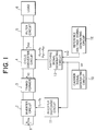
- a power conversion apparatus As shown in Fig. 1, a power conversion apparatus according to a first embodiment of the present invention is arranged in such a manner that a switching signal generating circuit 13 is employed in place of the switching signal generating circuit 13b employed in the conventional power conversion apparatus shown in Fig. 8.
- the switching signal generating circuit 13 comprises an absolute value circuit 102, a comparator 103, NOT circuits 105, 106, 108 and 110, 1/2 dividers 104 and 107, a polarity discriminating circuit 109, AND circuits 111 to 118 and OR circuits 119 to 126 so that switching signals P5 to P8 and P 5A to P 8A are transmitted.
- the above-described switching signals are respectively supplied to the corresponding switching devices S5 to S8 and S 5A to S 8A of the cyclo converter circuit 4.
- the reference voltage signal generating circuit 12 transmits the reference voltage signal Vcc* to be transmitted from the cyclo converter 4, the reference voltage signal Vcc* being, together with the carrier signal Vp, supplied to the switching signal generating circuit 13.
- the switching signal generating circuit 13 receives the above-described signals so as to transmit the switching signals T5 to T8 the pulse width of each which has been modulated as follows.
- the reference voltage signal Vcc* is converted into the absolute signal
- is, together with the carrier signal Vp, supplied to the comparator 103.
- the comparator 103 transmits the signal Tp shown in Fig.
- the signal Tp being then supplied to the 1/2 divider 104 in which the signal Tp is converted into the signal Ta.
- the signal Tp is supplied to the 1/2 divider 107 after the sign of it has been inverted by the NOT circuit 106, the signal Tb formed into the same wave shape as that of the signal Tx is transmitted.
- the signal Ta is supplied to the NOT circuit 105, the signal Tc is transmitted, while when the signal Tb is supplied to the NOT circuit 108, the signal Td formed into the same wave shape as that of the signal Ty is transmitted.
- the polarity discriminating circuit 109 transmits the polarity signal Vsgn denoting the polarity of the reference voltage signal Vcc.
- the NOT circuit 110 transmits a signal which is a signal obtainable by inverting the sign of the polarity signal Vsgn.
- the above-described signals and the signals Ta to Td are, via the AND circuits 111 to 118, supplied to the OR circuits 119 to 122.
- the signals T5 to T8 expressed by the above-described Equation B or D are respectively transmitted from the OR circuits 119 to 122.
- the logical sum of the signals T5 and Td is calculated in the OR circuit 123 so that the switching signal P5 shown in Fig. 3 is generated so as to be supplied to the switching device S5 of the cyclo converter circuit 4.
- the logical sum of the signals T5 and Tb, that of the signals T6 and Td and that of the signals T6 and Tb are calculated in the OR circuits 124 to 126 so that the switching signal P 5A , P6 and P 6A are generated so as to be supplied to the switching devices S 5A , S6 and S 6A .
- the signal T7 is as it is supplied to the switching devices S7 and S 7A as the switching signals P7 and P 7A . Furthermore, the signal T8 is as it is supplied to the switching devices S8 and S 8A as the switching signals P8 and P 8A .
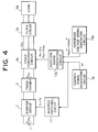
- Fig. 4 is a structural view which illustrates a second embodiment of the present invention.
- reference numeral 4a represents a three-phase cyclo converter circuit and 5a represents a three-phase filter circuit connected to the output terminal of the three-phase cyclo converter circuit 4a.
- Reference numeral 6a represents a three-phase load circuit connected to the output terminal of the three-phase filter circuit 5a.
- Reference numeral 12a represents a three-phase reference voltage signal generating circuit for generating a signal denoting the reference voltage which serves as a reference of the output voltage from the cyclo converter circuit 4a.
- Reference numeral 13a represents a switching signal generating circuit of the cyclo converter.
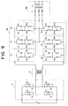
- Fig. 5 is a structural view which illustrates the detailed structures of the cyclo converter circuit 4a and the filter circuit 5a.
- the cyclo converter circuit 4a comprises switching devices S5 to S10 and S 5A to S 10A , diodes D5 to D10 and D 5A to D 10A connected to the above-described switching devices S5 to S10 and S 5A to S 10A in an anti-parallel manner.
- the filter circuit 5a is composed of three reactors L F and three capacitors C F .
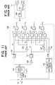
- Fig. 6 is a block diagram which illustrates the detailed structure of the switching signal generating circuit 13a.
- reference numerals 201 to 203 represent comparators and 204 to 206 and 211 represent 1/2 dividers which transmit output signals the polarity of each of which is inverted in synchronization with the last transition of the input signal.
- Reference numerals 207 to 210 and 212 represent NOT circuits and 213 to 224 represent OR circuits.
- the rectangular voltage V2 the duty ratio of which is 50% and which synchronizes with the carrier signal Vp, is transmitted from the transformer 3.
- the switching signal generating circuit 13a the carrier signal Vp and three-phase reference voltage signals Vccu*, Vccv* and Vccw* transmitted from the reference voltage signal generating circuit 12a are subjected to comparisons by the comparators 201 to 203 so that signals Tpu to Tpw are formed.
- the u-phase 1/2 divider 204 converts the signal Tpu into the signal T5 before the polarity of it is inverted by the NOT circuit 207 so that the signal T6 shown in Fig. 7 is obtained.
- the signal Tb which synchronizes with the carrier signal Vp is obtained.
- the polarity of the signal Tb is then inverted by the NOT circuit 212 so that the signal Td is obtained.
- the logical sum of the signals T5 and Td is calculated in the OR circuit 213 so that the switching signal P5 shown in Fig. 7 is generated so as to be supplied to the switching device S5 of the cyclo converter circuit 4a.
- the logical sum of the signals T5 and Tb, that of the signals T6 and Td and that of the signals T6 and Tb are calculated in the OR circuits 214 to 216 so that the switching signals P 5A , P6, and P 6A are generated so as to be supplied to the switching devices S 5A , S6 and S 6A .
- the switching signals P7, P 7A , P8 and P 8A are supplied to the v-phase switching devices S7, S 7A , S8 and S 8A from the OR circuits 217 to 220.
- Switching signals P9, P 9A , P10 and P 10A are supplied to w-phase switching devices S9, S 9A , S10 and S 10A from the OR circuits 221 to 224.
- the electric current passing through the portion corresponding to the inductance of the filter circuit 5a and the load circuit 6a is not cut off. Furthermore, no surge voltage is generated. Therefore, the necessity of using the great capacity snubber circuit for absorbing the surge voltage can be eliminated. Also at the other timing and in the other phases, the mode in which the passage for the electric current is opened can be eliminated so that similar effects can be obtained.
- the switch for the cyclo converter is constituted by the switching devices and the dioded.
- the present invention is not limited to this. Therefore, any switch which is capable of controlling the direction of the electric current may be employed to obtain the effect obtainable from the above-described embodiments.
Landscapes
- Engineering & Computer Science (AREA)
- Power Engineering (AREA)
- Inverter Devices (AREA)
- Ac-Ac Conversion (AREA)
Abstract
Description
- The present invention relates to a power conversion apparatus for use in an AC power source apparatus such as an uninterruptive power supply apparatus (hereinafter abbreviated to a "UPS") or a fuel cell generating system.
- Fig. 8 is a block diagram which illustrates a power conversion apparatus disclosed in, for example, Japanese Patent Application No. 1-211737. Referring to Fig.8,
reference numeral 1 represents a DC power source, 2 represents an inverter circuit and 3 represents a transformer the input terminal of which is connected to theinverter circuit 2.Reference numeral 4 represents a cyclo converter circuit connected to the output terminal of thetransformer 3.Reference numeral 5 represents a filter circuit connected to the output terminal of thecyclo converter circuit 4.Reference numeral 6 represents a load circuit, 10 represents a carrier signal generating circuit, 11 represents an inverter switching circuit, 12 represents a reference voltage signal generating circuit and 13b represents a switching signal generating circuit. - Fig. 9 illustrates the detailed structures of the
inverter circuit 2, thetransformer 3, thecyclo converter circuit 4 and thefilter circuit 5. Theinverter circuit 2 comprises switching devices S₁ to S₄ composed of transistors, MOSFETs or the like and diodes D₁ to D₄ which are respectively, in an anti-parallel manner, connected to the corresponding switching devices S₁ to S₄. Thetransformer 3 has a primary coil which is connected to theinverter circuit 2 and as well has a secondary coil which is connected to thecyclo converter circuit 4. Thecyclo converter circuit 4 comprises switching devices S₅ to S₈ and S5A to S8A composed of transistors, MOSFETs or the like and diodes D₅ to D₈ and D5A to D8A which are respectively, in an anti-parallel manner, connected to the corresponding switching devices S₅ to S₈ and S5A to S8A. The two semiconductor switching devices Sn and SnA (n = 5 to 8) and two diodes Dn and DnA (n = 5 to 8) connected to the same in the anti-parallel manner constitute a bidirectional switch Qn which is capable of controlling the power supply direction. - As shown in Fig. 10, the
inverter switching circuit 11 comprises a 1/2divider 100 which transmits an output signal, the polarity of which is inverted in synchronization with the last transition of an input signal, and aNOT circuit 101 connected to the 1/2divider 100. Theinverter switching circuit 11 transmits switching signals T₁ to T₄ to theinverter circuit 2, the signals T₁ to T₄ being signals for switching on/off the switching devices S₁ to S₄ of theinverter circuit 2. - Fig. 11 illustrates the detailed structure of the switching
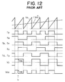
signal generating circuit 13b which comprises anabsolute value circuit 102, acomparator 103,NOT circuits dividing circuits discriminating circuit 109, ANDcircuits 111 to 118 andOR circuits 119 to 122. The switchingsignal generating circuit 13b transmits signals T₅ to T₈ which are signals for switching on/off switches Q₅ to Q₈ of thecyclo converter circuit 4. - Then, the operation of the above-described conventional apparatus will now be described with reference to a timing chart shown in Fig. 12. First, a sawtooth shape carrier signal Vp facing an upper right direction is transmitted from the carrier
signal generating circuit 10. Then, switching signals T₁ to T₄, the duty ratio of each of which is 50%, are transmitted from theinverter switching circuit 11 shown in Fig. 10. That is, when the carrier signal Vp is supplied, signal Tx, which synchronizes with the signal Vp and which is halved, is transmitted from the 1/2divider 100. Furthermore, theNOT circuit 101 transmits signal Ty which is a signal obtainable by inverting the sign of the signal Tx. As a result, the signal Tx is, as the switching signals T₁ and T₄, transmitted to theinverter circuit 2. Furthermore, the signal Ty is, as the switching signals T₂ and T₃, transmitted to the same. When the level of each of the switching signals T₁ to T₄ is high, the corresponding switching devices S₁ to S₄ of theinverter circuit 2 are switched on, while the same are switched off when the above-described level is low. Furthermore, the relationship between the switching on/off operations of the switching devices S₁ to S₄ and the secondary voltage V₂ of thetransformer 3 shown in Fig. 9 can be expressed as follows:


where symbol Vdc denotes the output voltage from theDC power source 1
Therefore, the secondary voltage V₂ becomes a rectangular wave voltage the duty ratio of which is 50% as shown in Fig. 12. - On the other hand, the reference voltage
signal generating circuit 12 transmits reference voltage signal Vcc* serving as a reference of the voltage to be transmitted from thecyclo converter 4, the reference voltage signal Vcc* being, together with the carrier signal Vp, supplied to the switchingsignal generating circuit 13b. The switchingsignal generating circuit 13b receives the above-described signals so as to transmit the switching signals T₅ to T₈ the pulse width of each which has been modulated as follows. Referring to Fig. 11, the reference voltage signal Vcc* is converted into absolute signal |Vcc*| by theabsolute value circuit 102. The absolute signal |Vcc*| is, together with the carrier signal Vp, supplied to thecomparator 103. Thecomparator 103 transmits signal Tp shown in Fig. 12, the signal Tp being then supplied to the 1/2divider 104 in which the signal Tp is converted into signal Ta. On the other hand, when the signal Tp is supplied to the 1/2divider 107 after the sign of it has been inverted by theNOT circuit 106, signal Tb formed into the same wave shape as that of the signal Tx is transmitted. Furthermore, when the signal Ta is supplied to theNOT circuit 105, signal Tc is transmitted, while when the signal Tb is supplied to theNOT circuit 108, signal Td formed into the same wave shape as that of the signal Ty is transmitted. - Then, the relationship between the signals Ta to Td and output voltage Vcc from the
cyclo converter circuit 4 will now be described. In a case where there is a desire to make the polarity of the output voltage Vcc to be positive, the switching signals T₅ to T₈ are determined in accordance with the following equations:

- In response to the above-described switching signals T₅ to T₈, the switch Qn (n = 5 to 8) which constitutes the bidirectional switch is switched on/off. As a result, the output voltage Vcc from the
cyclo converter circuit 4 is controlled. The fact that the switch Qn is switched on/off means a fact that the switching devices Sn and SnA are simultaneously switched on/off. The relationship between the switching on/off operation performed by the switch Qn (n = 5 to 8) and the above-described output voltage Vcc is expressed by the following equations:
- Therefore, the following facts can be deduced from Equations (B) and (C): when the levels of each of the signals Ta and Tb is high, the relationship Vcc = V₂ is held, when the levels of each of the signals Tc and Td is high, the relationship Vcc = - V₂ is held. When the levels of each of the signals Ta and Td or the signals Tb and Tc are high, the relationship Vcc = 0 is held. Therefore, the output voltage Vcc from the
cyclo converter circuit 4 is, as shown in Fig. 12, becomes positive voltage the pulse width of which has been modulated. In a case where there is a desire to make the polarity of the output voltage Vcc to be negative, the switching signals T₅ to T₈ may be determined in accordance with the following equations:

- Then, the description about the operation shown in Fig. 11 will now be continued. The polarity
discriminating circuit 109 transmits polarity signal Vsgn denoting the polarity of the reference voltage signal Vcc*. TheNOT circuit 110 transmits a signal which is a signal obtainable by inverting the sign of the polarity signal Vsgn. The above-described signals and the signals Ta to Td are, via theAND circuits 111 to 118, supplied to theOR circuits 119 to 122. When the polarity of the reference voltage signal Vcc* is positive, the signals Ta, Tc, Td and Tb are transmitted from theAND circuits cyclo converter circuit 4. Similarly, when the polarity of the reference voltage Vcc* is negative, the switching signals T₅ to T₈ in accordance with Equation (D) are transmitted to the switches Q₅ to Q₈. As a result of the above-described operations, the voltage Vcc, the wave form of which is obtainable by modulating the pulse width of the AC reference voltage signal Vcc* transmitted from the reference voltagesignal generating circuit 12, is transmitted from thecyclo converter circuit 4. Furthermore, by supplying the above-described output voltage to thefilter circuit 5 composed of a reactor LF and a capacitor CF as shown in Fig. 9, sine wave voltage from which the high frequency component has been removed by the pulse width modulation is supplied to theload circuit 6. - Since the conventional power conversion apparatus has been constituted as described above, there arises a problem in that undesirable surge voltage can be generated by energy stored in the circuit inductance because the electric passage is opened at the time of switching on/off the switching device of the
cyclo converter circuit 4. For example, at time t₁ shown in Fig. 12, a status in which the polarity of the voltage V₂ is positive, the switches Q₅ and Q₈ are switched on and thecyclo converter circuit 4 is transmitting the positive voltage Vcc is being shifted to a status in which the switch Q₅ is switched off, the switches Q₆ and Q₈ are switched on and thecyclo converter circuit 4 transmits zero voltage. - The switching device takes a certain definitely long time to be actually switched on/off. Therefore, the switch Q₆ must be switched on after the switch Q₅ has been switched off in order to prevent an operational mode in which the switches Q₅ and Q₆ are simultaneously switched on and thereby the secondary terminal of the
transformer 3 encounters a short circuit. However, since the circuit is temporarily opened during the shift from the switch Q₅ to the switch Q₆, the electric currents passing through the portions corresponding to the inductances of thefilter circuit 5 and theload circuit 6 are cut off. Therefore, surge voltage is generated, causing a problem to arise in that excessively large voltage to be applied to the switching device of thecyclo converter circuit 4 or theload circuit 6. - In order to overcome the above-described problem, an arrangement has been employed in which the switch Qn (n = 5 to 8) of the
cyclo converter circuit 4 is switched in only one direction as follows in accordance with the polarity of the output current from the cycle converter circuit so as to perform the pulse width modulation in a manner similar to the above-described structure. For example, when the polarity of the output current from thecyclo converter circuit 4 is positive, the switching signals T₅, T₆, T₇ and T₈ are respectively applied to the switching devices S₅, S6A, S7A and S₈ and as well as the residual switching devices S5A, S₆, S₇ and S8A are respectively switched off. When the polarity of the electric current is negative, the switching signals T₅, T₆, T₇ and T₈ are respectively applied to the switching devices S5A, S₆, S₇ and S8A and as well as the residual switching devices S₅, S6A, S7A and S₈ are respectively switched off. - However, the output current from the
cyclo converter circuit 4 contains a ripple component generated due to the pulse width modulation. Therefore, its polarity changes to positive or negative when the quantity of the electric current is insufficient. As a result, the above-described switch selection cannot be performed satisfactorily, causing a necessity to arise in that an open state is created in the cyclo converter. As a result, surge voltage will undesirably be generated. - Accordingly, a great capacity snubber circuit must be included in the conventional power conversion apparatus for the purpose of absorbing the surge voltage. What is even worse, the voltage rating of the switching device must be enlarged. Therefore, there arise a problem in that the size of the apparatus cannot be reduced or an excessively large loss is generated.
- Accordingly, an object of the present invention is to provide an apparatus capable of overcoming the above-described problems, preventing the generation of surge voltage, reducing the overall size and reducing a loss.
- In order to achieve the above objects, according to one aspect of the present invention, there is provided a power conversion apparatus comprising: an inverter circuit for converting DC power into AC power which has a first frequency; a transformer connected to the inverter circuit; a cyclo converter circuit having bidirectional switch means capable of controlling a direction in which an electric current passes and converting the output from the transformer into AC power which has a second frequency; and a switching signal generating circuit for generating a switching signal for controlling the polarity of the bidirectional switch means of the cyclo converter circuit in such a manner that the output voltage from the inverter circuit does not encounter a short circuit.
-
- Fig. 1 is a block diagram which illustrates a first embodiment of a power conversion apparatus according to the present invention;
- Fig. 2 is a block diagram which illustrates a switching signal generating circuit according to the first embodiment of the present invention;
- Fig. 3 is a timing chart which illustrates the operation of the first embodiment of the present invention;
- Fig. 4 is a block diagram which illustrates a second embodiment of the power conversion apparatus according to the present invention;
- Fig. 5 illustrates the circuit diagram of an inverter circuit, a transformer, a cyclo converter circuit and a filter circuit according to the second embodiment of the present invention;
- Fig. 6 is a block diagram which illustrates a switching signal generating circuit according to the second embodiment of the present invention;
- Fig. 7 is a timing chart which illustrates the operation of the second embodiment of the present invention;
- Fig. 8 is a block diagram which illustrates a conventional power conversion apparatus;
- Fig. 9 illustrates the circuit diagram of an inverter circuit, a transformer, a cyclo converter circuit and a filter circuit according to the conventional structure;
- Fig. 10 is a block diagram which illustrates an inverter switching circuit according to the conventional structure;
- Fig. 11 is a block diagram which illustrates a switching signal generating circuit according to the conventional structure; and
- Fig. 12 is a timing chart which illustrates the operation of the conventional structure.
- Preferred embodiments of the present invention will now be described with reference to the drawings.
- As shown in Fig. 1, a power conversion apparatus according to a first embodiment of the present invention is arranged in such a manner that a switching
signal generating circuit 13 is employed in place of the switchingsignal generating circuit 13b employed in the conventional power conversion apparatus shown in Fig. 8. - As shown in Fig. 2, the switching
signal generating circuit 13 comprises anabsolute value circuit 102, acomparator 103, NOTcircuits dividers polarity discriminating circuit 109, ANDcircuits 111 to 118 andOR circuits 119 to 126 so that switching signals P₅ to P₈ and P5A to P8A are transmitted. The above-described switching signals are respectively supplied to the corresponding switching devices S₅ to S₈ and S5A to S8A of thecyclo converter circuit 4. - Then, the operation of the first embodiment of the present invention thus-constituted will now be described with reference to a timing chart shown in Fig. 3. When the sawtooth shape carrier signal Vp facing an upper right direction is first transmitted from the carrier
signal generating circuit 10, the signal Tx and Ty, the duty ratio of each of which is 50%, are supplied from theinverter switching circuit 11 to theinverter circuit 2 as the switching signals T₁ to T₄ similarly to the conventional structure shown in Fig. 8. As a result, the rectangular voltage V₂, the duty ratio of which is 50%, is transmitted from thetransformer 3. - On the other hand, the reference voltage
signal generating circuit 12 transmits the reference voltage signal Vcc* to be transmitted from thecyclo converter 4, the reference voltage signal Vcc* being, together with the carrier signal Vp, supplied to the switchingsignal generating circuit 13. The switchingsignal generating circuit 13 receives the above-described signals so as to transmit the switching signals T₅ to T₈ the pulse width of each which has been modulated as follows. Referring to Fig. 11, the reference voltage signal Vcc* is converted into the absolute signal |Vcc*| by theabsolute value circuit 102. The absolute signal |Vcc*| is, together with the carrier signal Vp, supplied to thecomparator 103. Thecomparator 103 transmits the signal Tp shown in Fig. 12, the signal Tp being then supplied to the 1/2divider 104 in which the signal Tp is converted into the signal Ta. On the other hand, when the signal Tp is supplied to the 1/2divider 107 after the sign of it has been inverted by theNOT circuit 106, the signal Tb formed into the same wave shape as that of the signal Tx is transmitted. Furthermore, when the signal Ta is supplied to theNOT circuit 105, the signal Tc is transmitted, while when the signal Tb is supplied to theNOT circuit 108, the signal Td formed into the same wave shape as that of the signal Ty is transmitted. - Furthermore, the
polarity discriminating circuit 109 transmits the polarity signal Vsgn denoting the polarity of the reference voltage signal Vcc. In addition, theNOT circuit 110 transmits a signal which is a signal obtainable by inverting the sign of the polarity signal Vsgn. The above-described signals and the signals Ta to Td are, via the ANDcircuits 111 to 118, supplied to theOR circuits 119 to 122. In accordance with the polarity of the reference voltage signal Vcc, the signals T₅ to T₈ expressed by the above-described Equation B or D are respectively transmitted from theOR circuits 119 to 122. - As a result, the logical sum of the signals T₅ and Td is calculated in the
OR circuit 123 so that the switching signal P₅ shown in Fig. 3 is generated so as to be supplied to the switching device S₅ of thecyclo converter circuit 4. Similarly, the logical sum of the signals T₅ and Tb, that of the signals T₆ and Td and that of the signals T₆ and Tb are calculated in theOR circuits 124 to 126 so that the switching signal P5A, P₆ and P6A are generated so as to be supplied to the switching devices S5A, S₆ and S6A. - The signal T₇ is as it is supplied to the switching devices S₇ and S7A as the switching signals P₇ and P7A. Furthermore, the signal T₈ is as it is supplied to the switching devices S₈ and S8A as the switching signals P₈ and P8A.
- Then, the operation performed at time t₂ shown in Fig. 3 will now be described. At this time, the status in which the polarity of the voltage V₂ has been positive, the switches Q₅ and Q₈ have been switched on and the
cyclo converter circuit 4 has been transmitting positive voltage is being changed to a status in which the switch Q₅ is switched off, the switches Q₆ and Q₈ are switched on and thecyclo converter circuit 4 transmits zero voltage. An assumption is made here that the electric current passes in a positive direction through a route composed of the switching device S₅, the diode D5A, thefilter circuit 5, theload circuit 6, the switching device S₈ and the diode D8A in this sequential order. When the switching device S₅ is switched off in this state, passing of the electric current is continued due to the portion of the inductance of each of thefilter circuit 5 and theload circuit 6. However, since the switching-on signal has been supplied to the switching device S6A at this time, the above-described current is shifted to the switches S6A-D₆ so as to be circulated. Therefore, the electric current passing through the portion corresponding to the inductance is not cut off. Furthermore, no surge voltage is generated. Therefore, the necessity of using the great capacity snubber circuit for absorbing the surge voltage can be eliminated. - Then, a second embodiment of the present invention will now be described with reference to Figs. 4 to 7.
- Fig. 4 is a structural view which illustrates a second embodiment of the present invention. Referring to Fig. 4,
reference numeral 4a represents a three-phase cyclo converter circuit and 5a represents a three-phase filter circuit connected to the output terminal of the three-phasecyclo converter circuit 4a.Reference numeral 6a represents a three-phase load circuit connected to the output terminal of the three-phase filter circuit 5a.Reference numeral 12a represents a three-phase reference voltage signal generating circuit for generating a signal denoting the reference voltage which serves as a reference of the output voltage from thecyclo converter circuit 4a.Reference numeral 13a represents a switching signal generating circuit of the cyclo converter. - Fig. 5 is a structural view which illustrates the detailed structures of the
cyclo converter circuit 4a and thefilter circuit 5a. Thecyclo converter circuit 4a comprises switching devices S₅ to S₁₀ and S5A to S10A, diodes D₅ to D₁₀ and D5A to D10A connected to the above-described switching devices S₅ to S₁₀ and S5A to S10A in an anti-parallel manner. Thefilter circuit 5a is composed of three reactors LF and three capacitors CF. - Fig. 6 is a block diagram which illustrates the detailed structure of the switching
signal generating circuit 13a. Referring to Fig. 6,reference numerals 201 to 203 represent comparators and 204 to 206 and 211 represent 1/2 dividers which transmit output signals the polarity of each of which is inverted in synchronization with the last transition of the input signal.Reference numerals 207 to 210 and 212 represent NOT circuits and 213 to 224 represent OR circuits. - Then, the operation of the second embodiment will now be described with reference to a timing chart shown in Fig. 7.
- Similarly to the first embodiment, the rectangular voltage V₂, the duty ratio of which is 50% and which synchronizes with the carrier signal Vp, is transmitted from the
transformer 3. On the other hand, in the switchingsignal generating circuit 13a, the carrier signal Vp and three-phase reference voltage signals Vccu*, Vccv* and Vccw* transmitted from the reference voltagesignal generating circuit 12a are subjected to comparisons by thecomparators 201 to 203 so that signals Tpu to Tpw are formed. The u-phase 1/2divider 204 converts the signal Tpu into the signal T₅ before the polarity of it is inverted by theNOT circuit 207 so that the signal T₆ shown in Fig. 7 is obtained. In the 1/2divider 211 to which the w-phase signal Tpw has been supplied after its polarity had been inverted by theNOT circuit 210, the signal Tb which synchronizes with the carrier signal Vp is obtained. The polarity of the signal Tb is then inverted by theNOT circuit 212 so that the signal Td is obtained. - As a result, the logical sum of the signals T₅ and Td is calculated in the
OR circuit 213 so that the switching signal P₅ shown in Fig. 7 is generated so as to be supplied to the switching device S₅ of thecyclo converter circuit 4a. Similarly, the logical sum of the signals T₅ and Tb, that of the signals T₆ and Td and that of the signals T₆ and Tb are calculated in theOR circuits 214 to 216 so that the switching signals P5A, P₆, and P6A are generated so as to be supplied to the switching devices S5A, S₆ and S6A. - Similarly to the u-phase, the switching signals P₇, P7A, P₈ and P8A are supplied to the v-phase switching devices S₇, S7A, S₈ and S8A from the
OR circuits 217 to 220. Switching signals P₉, P9A, P₁₀ and P10A are supplied to w-phase switching devices S₉, S9A, S₁₀ and S10A from theOR circuits 221 to 224. - Then, the operation to be performed at time t₃ shown in Fig. 7 will now be described. At this time, a status in which the polarity of the voltage V₂ is positive, the switch Q₅ has been switched on so that positive voltage Vccu is transmitted on the basis of an imaginary neutral point, for example, the middle point of the secondary coil of the
transformer 3 is being shifted to a status in which the switch Q₅ is switched off and as well as the switch Q₆ is switched on so that negative voltage Vccu is transmitted. An assumption is made here that the electric current passes in a positive direction from the switching device S₅-diode D5A to thefilter circuit 5a at this time. When the switch Q₅ is switched off in this state, the electric current which has passed through the switching device S₅ is shifted to the switch S6A-D₆ to which the switching-on signal has been supplied at this time. - Therefore, the electric current passing through the portion corresponding to the inductance of the
filter circuit 5a and theload circuit 6a is not cut off. Furthermore, no surge voltage is generated. Therefore, the necessity of using the great capacity snubber circuit for absorbing the surge voltage can be eliminated. Also at the other timing and in the other phases, the mode in which the passage for the electric current is opened can be eliminated so that similar effects can be obtained. - According to the above-described embodiments, the switch for the cyclo converter is constituted by the switching devices and the dioded. However, the present invention is not limited to this. Therefore, any switch which is capable of controlling the direction of the electric current may be employed to obtain the effect obtainable from the above-described embodiments.
Claims (6)
- A power conversion apparatus comprising:
an inverter circuit for converting DC power into AC power which has a first frequency;
a transformer connected to said inverter circuit;
a cyclo converter circuit having bidirectional switch means capable of controlling a direction in which an electric current passes and converting the output from said transformer into AC power which has a second frequency; and
a switching signal generating circuit for generating a switching signal for controlling the polarity of said bidirectional switch means of said cyclo converter circuit in such a manner that the output voltage from said inverter circuit does not encounter a short circuit. - An apparatus according to Claim 1 further comprising:
a carrier signal generating circuit for generating a carrier signal having a predetermined frequency;
an inverter switching circuit for generating a signal for controlling said inverter circuit in synchronization with said carrier signal; and
a reference voltage signal generating circuit for generating a reference signal for AC voltage to be transmitted from said cyclo converter circuit,
said switching signal generating circuit generating a switching signal in response to the carrier signal transmitted from said carrier signal generating circuit and the reference voltage signal transmitted from said reference voltage signal generating circuit. - An apparatus according to Claim 1 wherein said bidirectional switch means of said cyclo converter circuit comprises a plurality of bidirectional switches each having a pair of switches each of which is arranged to pass an electric current in opposing directions, said switching signal generating circuit generating a switching signal for always switching on either of said pair of bidirectional switches which has a polarity which does not cause the output voltage from said inverter circuit to encounter a short circuit.
- An apparatus according to Claim 3 wherein said switching signal generating circuit transmits a switching signal which corresponds to each switch of said bidirectional switch means of said cyclo converter circuit and as well as the pulse width of which has been modulated.
- An apparatus according to Claim 1 further comprising a filter circuit for removing a high frequency component contained in the output from said cyclo converter circuit.
- An apparatus according to Claim 1 wherein said inverter circuit transmits AC power the duty ratio of which is 50%.
Applications Claiming Priority (2)
| Application Number | Priority Date | Filing Date | Title |
|---|---|---|---|
| JP2279895A JP2598163B2 (en) | 1990-10-16 | 1990-10-16 | Power converter |
| JP279895/90 | 1990-10-16 |
Publications (3)
| Publication Number | Publication Date |
|---|---|
| EP0481456A2 true EP0481456A2 (en) | 1992-04-22 |
| EP0481456A3 EP0481456A3 (en) | 1992-07-08 |
| EP0481456B1 EP0481456B1 (en) | 1997-01-02 |
Family
ID=17617424
Family Applications (1)
| Application Number | Title | Priority Date | Filing Date |
|---|---|---|---|
| EP91117655A Expired - Lifetime EP0481456B1 (en) | 1990-10-16 | 1991-10-16 | Power conversion apparatus |
Country Status (6)
| Country | Link |
|---|---|
| US (1) | US5274538A (en) |
| EP (1) | EP0481456B1 (en) |
| JP (1) | JP2598163B2 (en) |
| KR (1) | KR920009035A (en) |
| CA (1) | CA2053381C (en) |
| DE (1) | DE69123928T2 (en) |
Cited By (1)
| Publication number | Priority date | Publication date | Assignee | Title |
|---|---|---|---|---|
| EP0487970A2 (en) * | 1990-11-28 | 1992-06-03 | Hitachi, Ltd. | Power conversion system, method for controlling the same, and uninterruptible power supply using the same |
Families Citing this family (17)
| Publication number | Priority date | Publication date | Assignee | Title |
|---|---|---|---|---|
| CA2192891C (en) * | 1996-01-16 | 2000-02-22 | Jon O. Reynolds | Plasma cutting or arc welding power supply with phase staggered secondary switchers |
| US20100244773A1 (en) * | 2009-03-27 | 2010-09-30 | Gm Global Technology Operations, Inc. | Unity power factor isolated single phase matrix converter battery charger |
| US8199545B2 (en) * | 2009-05-05 | 2012-06-12 | Hamilton Sundstrand Corporation | Power-conversion control system including sliding mode controller and cycloconverter |
| US8466658B2 (en) * | 2009-08-05 | 2013-06-18 | GM Global Technology Operations LLC | Systems and methods for bi-directional energy delivery with galvanic isolation |
| US8462528B2 (en) | 2010-07-19 | 2013-06-11 | GM Global Technology Operations LLC | Systems and methods for reducing transient voltage spikes in matrix converters |
| US8467197B2 (en) | 2010-11-08 | 2013-06-18 | GM Global Technology Operations LLC | Systems and methods for compensating for electrical converter nonlinearities |
| US8599577B2 (en) * | 2010-11-08 | 2013-12-03 | GM Global Technology Operations LLC | Systems and methods for reducing harmonic distortion in electrical converters |
| US8587962B2 (en) | 2010-11-08 | 2013-11-19 | GM Global Technology Operations LLC | Compensation for electrical converter nonlinearities |
| US8614564B2 (en) | 2010-11-18 | 2013-12-24 | GM Global Technology Operations LLS | Systems and methods for providing power to a load based upon a control strategy |
| CN103314516A (en) * | 2011-01-04 | 2013-09-18 | 恩菲斯能源公司 | Method and apparatus for resonant power conversion |
| US8860379B2 (en) | 2011-04-20 | 2014-10-14 | GM Global Technology Operations LLC | Discharging a DC bus capacitor of an electrical converter system |
| EP2715926A4 (en) * | 2011-05-26 | 2015-09-02 | Enphase Energy Inc | Method and apparatus for generating single-phase power from a three-phase resonant power converter |
| US8829858B2 (en) | 2011-05-31 | 2014-09-09 | GM Global Technology Operations LLC | Systems and methods for initializing a charging system |
| US8878495B2 (en) | 2011-08-31 | 2014-11-04 | GM Global Technology Operations LLC | Systems and methods for providing power to a load based upon a control strategy |
| US9770991B2 (en) | 2013-05-31 | 2017-09-26 | GM Global Technology Operations LLC | Systems and methods for initializing a charging system |
| WO2014203282A2 (en) * | 2013-06-20 | 2014-12-24 | Kraftpowercon India Private Limited | Ac/ac converter for conversion between three phase and single phase power supplies |
| CN112350557B (en) * | 2020-09-21 | 2022-05-24 | 珠海万力达电气自动化有限公司 | Control method for improving continuous operation capacity under impact current of railway purification power supply |
Family Cites Families (15)
| Publication number | Priority date | Publication date | Assignee | Title |
|---|---|---|---|---|
| US3487289A (en) * | 1968-04-16 | 1969-12-30 | Gen Electric | Multipurpose power converter circuits |
| US3742336A (en) * | 1971-11-24 | 1973-06-26 | Gen Electric | Versatile cycloinverter power converter circuits |
| US4479175A (en) * | 1982-08-13 | 1984-10-23 | Honeywell Inc. | Phase modulated switchmode power amplifier and waveform generator |
| JPS59178975A (en) * | 1983-03-29 | 1984-10-11 | Mitsubishi Electric Corp | Inverter |
| US4556937A (en) * | 1983-10-05 | 1985-12-03 | Canadian Patents And Development Limited | DC-AC Power converter including two high frequency resonant link converters |
| JPS6176069A (en) * | 1984-09-20 | 1986-04-18 | Mitsubishi Electric Corp | Converter device |
| JPS61173636A (en) * | 1984-12-18 | 1986-08-05 | 三菱電機株式会社 | Power source unit |
| JPH0810986B2 (en) * | 1985-06-17 | 1996-01-31 | 株式会社日立製作所 | Power converter |
| JPS6268068A (en) * | 1985-09-20 | 1987-03-27 | Mitsubishi Electric Corp | Power converter |
| US4719550A (en) * | 1986-09-11 | 1988-01-12 | Liebert Corporation | Uninterruptible power supply with energy conversion and enhancement |
| EP0293869B1 (en) * | 1987-06-05 | 1993-09-01 | Hitachi, Ltd. | Power conversion system |
| JPH0746906B2 (en) * | 1987-08-17 | 1995-05-17 | 三菱電機株式会社 | Voltage converter |
| EP0309919B1 (en) * | 1987-09-30 | 1993-01-20 | Hitachi, Ltd. | A power conversion apparatus |
| JPH0783615B2 (en) * | 1988-11-28 | 1995-09-06 | 三菱電機株式会社 | Three-phase converter |
| US5159539A (en) * | 1989-08-17 | 1992-10-27 | Mitsubishi Denki Kabushiki Kaisha | High frequency DC/AC power converting apparatus |
-
1990
- 1990-10-16 JP JP2279895A patent/JP2598163B2/en not_active Expired - Fee Related
-
1991
- 1991-09-30 KR KR1019910017094A patent/KR920009035A/en not_active Application Discontinuation
- 1991-10-11 CA CA002053381A patent/CA2053381C/en not_active Expired - Fee Related
- 1991-10-15 US US07/775,607 patent/US5274538A/en not_active Expired - Fee Related
- 1991-10-16 DE DE69123928T patent/DE69123928T2/en not_active Expired - Fee Related
- 1991-10-16 EP EP91117655A patent/EP0481456B1/en not_active Expired - Lifetime
Non-Patent Citations (2)
| Title |
|---|
| Ikuo Yamato: "HIGH FREQUENCY LINK DC-AC CONVERTER FOR UPS WITH A NEW VOLTAGE CLAMPER" PESC'90, RECORD Vol. II, 21st Annual IEEE Power Electronics Specialists Conference, San Antonio, Texas, June 11-14, 1990, pages 749-756. * |
| Takao Kawabata: "HIGH FREQUENCY LINK DC/AC CONVERTER WITH PWM CYCLOCONVERTER" Conference record of the 1990 IEEE Industry Applications Society Annual Meeting, Part II. Papers presented at the 1990 Industry Applications Conference Twenty-Fifth IAS Annual Meeting The Westing Hotel Seattle, Washinton October 7-12, 1990 pages 1119-1124 * |
Cited By (3)
| Publication number | Priority date | Publication date | Assignee | Title |
|---|---|---|---|---|
| EP0487970A2 (en) * | 1990-11-28 | 1992-06-03 | Hitachi, Ltd. | Power conversion system, method for controlling the same, and uninterruptible power supply using the same |
| EP0487970A3 (en) * | 1990-11-28 | 1992-09-02 | Hitachi, Ltd. | Power conversion system, method for controlling the same, and uninterruptible power supply using the same |
| US5285365A (en) * | 1990-11-28 | 1994-02-08 | Hitachi, Ltd. | Power conversion system, method for controlling the same, and uninterruptible power supply using the same |
Also Published As
| Publication number | Publication date |
|---|---|
| EP0481456B1 (en) | 1997-01-02 |
| DE69123928T2 (en) | 1997-05-15 |
| KR920009035A (en) | 1992-05-28 |
| DE69123928D1 (en) | 1997-02-13 |
| CA2053381C (en) | 1998-02-17 |
| EP0481456A3 (en) | 1992-07-08 |
| JPH04156274A (en) | 1992-05-28 |
| US5274538A (en) | 1993-12-28 |
| JP2598163B2 (en) | 1997-04-09 |
| CA2053381A1 (en) | 1992-04-17 |
Similar Documents
| Publication | Publication Date | Title |
|---|---|---|
| EP0481456A2 (en) | Power conversion apparatus | |
| EP0475345B1 (en) | AC/DC power converting apparatus | |
| Kawabata et al. | High frequency link DC/AC converter with PWM cycloconverter | |
| US5159539A (en) | High frequency DC/AC power converting apparatus | |
| US5694307A (en) | Integrated AC/DC and DC/DC converter | |
| US5930122A (en) | Inverter and DC power supply apparatus with inverter used therein | |
| KR910007224A (en) | AC-DC-AC Power Converter | |
| WO1986004749A1 (en) | Multiphase dc-dc series-resonant converter | |
| US6728120B1 (en) | Rectifier apparatus for high voltages | |
| CA2054319C (en) | Power supply unit for arc processing | |
| EP1450476B1 (en) | Power converter circuit | |
| ES2103668A1 (en) | Uninterruptible power supply system | |
| JP2002517150A (en) | Energy converter and uninterruptible power supply (UPS) using the same | |
| US4811185A (en) | DC to DC power converter | |
| US7095634B2 (en) | Arc welding set with power source and inverter | |
| US4639850A (en) | Power converter device | |
| EP0503631B1 (en) | High frequency link power conversion apparatus | |
| US20050078497A1 (en) | Three phase isolated vector switching AC to AC frequency converters | |
| KR930006388B1 (en) | Dc/ac converter | |
| US4888676A (en) | Damping circuit for turn-off valves | |
| JP3080542B2 (en) | Inverter system of carrier frequency modulation by high frequency transformer coupling | |
| KR960006374Y1 (en) | Power conversion apparatus | |
| CN113364333B (en) | Combined current converter, direct current transformer and control method | |
| CN216851782U (en) | Bidirectional power supply | |
| JPH066976A (en) | Power converter and uninterruptible power supply |
Legal Events
| Date | Code | Title | Description |
|---|---|---|---|
| PUAI | Public reference made under article 153(3) epc to a published international application that has entered the european phase |
Free format text: ORIGINAL CODE: 0009012 |
|
| AK | Designated contracting states |
Kind code of ref document: A2 Designated state(s): DE FR GB |
|
| PUAL | Search report despatched |
Free format text: ORIGINAL CODE: 0009013 |
|
| AK | Designated contracting states |
Kind code of ref document: A3 Designated state(s): DE FR GB |
|
| 17P | Request for examination filed |
Effective date: 19920916 |
|
| 17Q | First examination report despatched |
Effective date: 19940301 |
|
| GRAG | Despatch of communication of intention to grant |
Free format text: ORIGINAL CODE: EPIDOS AGRA |
|
| GRAH | Despatch of communication of intention to grant a patent |
Free format text: ORIGINAL CODE: EPIDOS IGRA |
|
| GRAH | Despatch of communication of intention to grant a patent |
Free format text: ORIGINAL CODE: EPIDOS IGRA |
|
| GRAA | (expected) grant |
Free format text: ORIGINAL CODE: 0009210 |
|
| AK | Designated contracting states |
Kind code of ref document: B1 Designated state(s): DE FR GB |
|
| REF | Corresponds to: |
Ref document number: 69123928 Country of ref document: DE Date of ref document: 19970213 |
|
| ET | Fr: translation filed | ||
| PLBE | No opposition filed within time limit |
Free format text: ORIGINAL CODE: 0009261 |
|
| STAA | Information on the status of an ep patent application or granted ep patent |
Free format text: STATUS: NO OPPOSITION FILED WITHIN TIME LIMIT |
|
| 26N | No opposition filed | ||
| REG | Reference to a national code |
Ref country code: GB Ref legal event code: IF02 |
|
| PGFP | Annual fee paid to national office [announced via postgrant information from national office to epo] |
Ref country code: FR Payment date: 20041008 Year of fee payment: 14 |
|
| PGFP | Annual fee paid to national office [announced via postgrant information from national office to epo] |
Ref country code: GB Payment date: 20041013 Year of fee payment: 14 |
|
| PGFP | Annual fee paid to national office [announced via postgrant information from national office to epo] |
Ref country code: DE Payment date: 20041014 Year of fee payment: 14 |
|
| PG25 | Lapsed in a contracting state [announced via postgrant information from national office to epo] |
Ref country code: GB Free format text: LAPSE BECAUSE OF NON-PAYMENT OF DUE FEES Effective date: 20051016 |
|
| PG25 | Lapsed in a contracting state [announced via postgrant information from national office to epo] |
Ref country code: DE Free format text: LAPSE BECAUSE OF NON-PAYMENT OF DUE FEES Effective date: 20060503 |
|
| GBPC | Gb: european patent ceased through non-payment of renewal fee |
Effective date: 20051016 |
|
| PG25 | Lapsed in a contracting state [announced via postgrant information from national office to epo] |
Ref country code: FR Free format text: LAPSE BECAUSE OF NON-PAYMENT OF DUE FEES Effective date: 20060630 |
|
| REG | Reference to a national code |
Ref country code: FR Ref legal event code: ST Effective date: 20060630 |