EP0262812A2 - Buck-boost parallel resonant converter - Google Patents
Buck-boost parallel resonant converter Download PDFInfo
- Publication number
- EP0262812A2 EP0262812A2 EP87307811A EP87307811A EP0262812A2 EP 0262812 A2 EP0262812 A2 EP 0262812A2 EP 87307811 A EP87307811 A EP 87307811A EP 87307811 A EP87307811 A EP 87307811A EP 0262812 A2 EP0262812 A2 EP 0262812A2
- Authority
- EP
- European Patent Office
- Prior art keywords
- converter
- voltage
- inductor
- control
- output
- Prior art date
- Legal status (The legal status is an assumption and is not a legal conclusion. Google has not performed a legal analysis and makes no representation as to the accuracy of the status listed.)
- Granted
Links
Images


Classifications
-
- H—ELECTRICITY
- H02—GENERATION; CONVERSION OR DISTRIBUTION OF ELECTRIC POWER
- H02M—APPARATUS FOR CONVERSION BETWEEN AC AND AC, BETWEEN AC AND DC, OR BETWEEN DC AND DC, AND FOR USE WITH MAINS OR SIMILAR POWER SUPPLY SYSTEMS; CONVERSION OF DC OR AC INPUT POWER INTO SURGE OUTPUT POWER; CONTROL OR REGULATION THEREOF
- H02M3/00—Conversion of dc power input into dc power output
- H02M3/22—Conversion of dc power input into dc power output with intermediate conversion into ac
- H02M3/24—Conversion of dc power input into dc power output with intermediate conversion into ac by static converters
- H02M3/28—Conversion of dc power input into dc power output with intermediate conversion into ac by static converters using discharge tubes with control electrode or semiconductor devices with control electrode to produce the intermediate ac
- H02M3/325—Conversion of dc power input into dc power output with intermediate conversion into ac by static converters using discharge tubes with control electrode or semiconductor devices with control electrode to produce the intermediate ac using devices of a triode or a transistor type requiring continuous application of a control signal
- H02M3/335—Conversion of dc power input into dc power output with intermediate conversion into ac by static converters using discharge tubes with control electrode or semiconductor devices with control electrode to produce the intermediate ac using devices of a triode or a transistor type requiring continuous application of a control signal using semiconductor devices only
- H02M3/337—Conversion of dc power input into dc power output with intermediate conversion into ac by static converters using discharge tubes with control electrode or semiconductor devices with control electrode to produce the intermediate ac using devices of a triode or a transistor type requiring continuous application of a control signal using semiconductor devices only in push-pull configuration
- H02M3/3372—Conversion of dc power input into dc power output with intermediate conversion into ac by static converters using discharge tubes with control electrode or semiconductor devices with control electrode to produce the intermediate ac using devices of a triode or a transistor type requiring continuous application of a control signal using semiconductor devices only in push-pull configuration of the parallel type
-
- Y—GENERAL TAGGING OF NEW TECHNOLOGICAL DEVELOPMENTS; GENERAL TAGGING OF CROSS-SECTIONAL TECHNOLOGIES SPANNING OVER SEVERAL SECTIONS OF THE IPC; TECHNICAL SUBJECTS COVERED BY FORMER USPC CROSS-REFERENCE ART COLLECTIONS [XRACs] AND DIGESTS
- Y02—TECHNOLOGIES OR APPLICATIONS FOR MITIGATION OR ADAPTATION AGAINST CLIMATE CHANGE
- Y02B—CLIMATE CHANGE MITIGATION TECHNOLOGIES RELATED TO BUILDINGS, e.g. HOUSING, HOUSE APPLIANCES OR RELATED END-USER APPLICATIONS
- Y02B70/00—Technologies for an efficient end-user side electric power management and consumption
- Y02B70/10—Technologies improving the efficiency by using switched-mode power supplies [SMPS], i.e. efficient power electronics conversion e.g. power factor correction or reduction of losses in power supplies or efficient standby modes
Definitions
- the present invention relates to a switching power supply and more particularly to a switchmode converter circuit having a parallel resonant circuit topology and a capability to operate in both buck and boost modes.
- a converter circuit is used for producing one or more regulated DC output DC voltages of desired values.
- the converter generates the regulated output DC voltages from a DC line voltage (DC-DC conversion) or from an AC line voltage (AC-DC).
- DC-DC conversion DC line voltage
- AC-DC AC line voltage
- an input rectifier is provided for rectifying the input AC line voltage to the unregulated DC voltage that is used by the converter.
- switchmode converters operate by switching a DC input line voltage between two primary windings of a transformer which are wound out of phase with one another .
- the resulting output at the secondary winding is an AC pulse width modulated rectangular wave signal having an output magnitude which is related to the primary voltage by the turns ratio between the secondary and primary windings.
- This AC signal, at the secondary winding is rectified, for example by passing it through a full wave rectifier bridge and capacitor filter combination, to obtain an essentially ripple-free output DC voltage. Additional secondary windings are provided if more than one DC outputs are needed.
- the magnitude of the output DC voltage with respect to the primary voltage is established primarily by the turns ratio between the secondary and primary windings. It is however also affected by the voltage or current that is impressed on or through the primary windings.
- At least one of the outputs is constantly monitored and conditions at the primary are controlled to assure that the output remains within its set limits.
- the typical specification of a power supply includes the definition of the following items: The nominal output voltages; The minimum and maximum load currents; The load regulation, e.g. the change in the output voltages for a specified change in any or all of the load currents; The line regulation, e.g. the allowed change in the output voltages for a specified change in the input voltage; The cross regulation, e.g. the allowed change in one specific output voltage when the current in other than this specified output is changed by a specified amount; The input line compliance, e.g. the ratio of the maximum to the minimum input line voltage over which the converter is capable of providing the specified performance.
- the AC line voltage is rectified by a bridge rectifier circuit to produce an unregulated input DC voltage.
- the unregulated DC voltage has an average or DC value which is subject to AC line voltage fluctuations.
- a DC input filter receives and filters the input DC voltage to reduce or eliminate ripple voltages therefrom. Thereafter a converter circuit is provided for producing a DC output voltage from the input DC voltage.
- the converter "chops" the input DC voltage to produce AC voltage signals at secondary windings of an output transformer.
- the AC voltage signals at the secondaries are converted to the regulated output DC voltages in the output stage.
- An output stage includes rectifier and output filtering elements for the output DC voltages.
- a controller circuit in the DC-AC stage samples and monitors the output DC voltages and controls the voltage or current flowing through the primary windings of the output transformer to assure that the output DC voltages remain within certain set limits.
- FIG. 1 of the drawings A typical converter arrangement is shown in Fig. 1 of the drawings.
- -"Switchmode refers to a converter which is based on “chopping" the DC input voltage at a high frequency (typically higher than 50 khz) to convert it to a pulse width modulated AC rectangular waveform having the desired average value.
- This technique must include a rectifying block to convert the AC to unfiltered DC, and must include an averaging output filter (usually an LC filer) to reduce the chopping frequency related ripple voltage to within the desired values.
- -"Sampling frequency refers to the frequency at which the controller samples and adjusts the output voltages.
- Control bandwidth frequency refers to the bandwidth of the feedback control loop. This control bandwidth determines the upper frequency limit for which the control circuit can reduce the influence of disturbing signals.
- Voltage mode refers to a switchmode converter wherein the pulse width is controlled, and the current driving the primary of the transformer is influenced by other parameters such as input voltage and output filter inductance value.
- -"Current mode refers to a switchmode converter wherein the instantaneous current in the filter inductor is controlled independent of the other variables which influence this current in the voltage mode topology.
- Continuous/discontinuous current switching is used to denote a converter in which, respectively, the current flowing through the primary winding is continuous or discontinuous.
- a discontinuous switcher the current through the primary drops to zero before the end of each control period.
- -"Zero current turn off is related to a "discontinuous current switching converter" and denotes the fact that the current through the switching element has subsided before certain switching elements in the converter are turned on or off.
- Paraallel resonance converter refers to converters in which a parallel resonant circuit is used.
- -'Q multiplication is meaningful in relation to converters using resonant circuits and refers to the inherent ability of a resonant converter to develop a voltage which is several; i.e. "Q" times larger than in input voltage to which the resonant circuit is connected.
- -"Buck mode refers to a converter in which the operating voltage at the primary winding of the converter is lower than the input voltage supplied to the converter.
- -"Boost mode is similar to buck mode except that the voltage at the primary is higher than the input voltage.
- the present invention is directed to a novel and unique switchmode converter which employs a parallel resonant circuit topology and operates at a fixed frequency.
- the invention features a unique input coupled inductor that will be described in detail later herein.
- the input coupled inductor is adapted to divert energy stored in this inductor at the end of a switching cycle back to the input DC voltage source and to prevent dissipation of that inductive energy in the switching elements of the converter. Regulation of the output DC voltages respect to a voltage waveform that is generated by the converter's resonant components.
- the control signal adjusts output by pulse width modulation of the switching elements in the converter.
- Series resonant converters do provide certain advantages. They minimise turn on switching transient currents in the switching elements and in the output rectifiers. Anther advantage relates to cases where such series resonant converters are operated in a discontinuous mode. In the latter case the losses int he switching elements are minimised and the series topology enables the use of SCR's for the switching elements.
- a series resonant converter can be operated in a continuous current mode wherein the next switching cycle is turned on before current from a previous cycle has ceased. But the continuous mode loses the benefit of operating the switching elements when the current is equal to zero, and efficiency suffers. Furthermore, although the continuous mode of operaton provides the advantage of higher power density, i.e. more power is generated from a given converter size, the allowable range of the controlling frequency is smaller. Therefore, the dynamic control range of the output power is accordingly limited.
- a converter which has the familiar functional blocks of a switchmode power supply including for example an input rectifier and filter circuit which receives AC power and converts that power to an unregulated DC voltage.
- a DC-AC circuit block of the converter is responsive to the DC input voltage to generate therefrom one or more AC signals of different magnitudes.
- Output rectifier and filter circuits rectify the AC signals generated in the DC-AC stage to one or more DC output voltages which are suitable for driving loads.
- a controller in the DC-AC block samples at least one of the DC output voltages and adjusts the electrical conditions in the DC-AC stage to assure that the output DC voltages remain within prescribed voltage and/or current limits.
- the present invention is specifically directed to a novel converter which includes a parallel resonant circuit topology which is configured to advantageously harness the stray capacitance in the converter.
- a novel coupled inductor circuit is included which enables residual energy in the resonant circuit at the end of each switching cycle to be returned to its source.
- the converter operates at a fixed control frequency.
- a controller circuit of the DC-AC stage regulates the current flowing in the windings of the primary during each control cycle so that just enough current is delivered to an "output rectifier and filter" circuit block to maintain the DC output voltages within their limits irrespective of and despite load and input line fluctuations.
- the control frequency is relatively high, normally in the 50 to 500 kilohertz range. This yields a control bandwidth which is high enough to electronically regulate out line frequency related ripple voltages that may be present at the input end of the converter.
- the high control bandwidth provides, in addition, inherent short circuit protection since the fast and highly responsive control is able to shut off the converter before sensitive electrical components are damaged.
- the converter of the invention may be operated in a continuous or discontinuous mode and it will automatically transit between buck and boost modes as required by the conditions of operation.
- the coupled inductor includes a resonating inductor winding and an energy recovery inductor winding which are tightly wound and out of phase with one anther.
- the windings of the coupled inductor are connected to the input DC voltage directly or indirectly through an input filter.
- the resonating inductor winding is connected to the centre tap of an output transformer having a primary with first and second coupled and also out of phase windings.
- Each of the primary windings is connected in series with respective diode and a switching element.
- the switching comprises a transistor or the like having one terminal, i.e. for bipolar transistors, emitter or collector which is connected to the return (ground) line.
- a resonating capacitor is connected across the primary windings of the output transformer.
- One or more secondary windings of the output transformer have a turns ratio which is selected to produce an AC voltage/current signal of a magnitude needed for the DC output voltages.
- a respective full wave rectifier bridge is connected to each secondary winding to convert its AC signal to a DC output in the conventional manner.
- a fixed frequency pulse width modulation controller of known type samples and compares the value of one of the DC outputs to an internal reference.
- An error signal is then delivered which adjusts the current flowing through the primary windings by varying the instant at which the switching elements connected in series with the primary windings are turned on and off. Thereby the voltage magnitudes of the DC outputs are maintained within specified limits.
- the converter topology of the present invention offers several distinct advantages over prior art converters.
- the resonating capacitor connected across the primary windings and the stray capacitance of the converter are in parallel to one another. Consequently, the resonant freqency of the parallel resonance converter is determined by the values of the coupled inductor winding, the resonating capacitor, the stray capacitance and to a lesser extent by the inductance of the primary winding. Therefore, instead of constituting a troublesome and energy dissipating element, the stray capacitance is turned into an asset by becoming part of the capacitor portion of the parallel resonance circuit.
- the converter can be operated at higher frequencies.
- the higher frequencies in turn, produce a very high control bandwidth, providing a tight and fast control response. Consequently, the controller is itself capable of reducing or eliminating high frequency ripple voltages which simplifies the design of the output filter.
- the fast response provides an inherent short-circuit protection capacility as the converter can sense and shut-down the converter before sensitive electrical components are damaged during short circuit conditions.
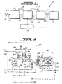
- FIG. 1 The basic block diagram of a switchmode converter is illustrated in Fig. 1.
- a power converter 10 of the present invention is responsive to AC input power from a voltage source 12.
- the AC power which may be single phase or multi phase is received by input rectifier and filter block 14 which rectifies the AC power to produce at output 18 thereof an input line DC voltage 16.
- Input rectifier and filter block 14 is of the known type and may include bridge rectifiers for rectifying the AC output, an LC filter for filtering and storing rectified power and appropriate EMI circuitry for reducing electomagnetic radiation into the AC supply 12 and/or into the environment.
- Input line DC voltage 16 is supplied to DC-AC converter 20 in which the input line voltage is "chopped” to produce an AC signal waveform 22 at an output 24.
- the peak to peak magnitude of AC signal 22 is primarily set by the turns ratio of a transformer in the DC-AC converter 20.
- the tunrs ratio is selected so the rectification of AC signal 22 in output rectifier and filter circuit 26 produces at output 30 an output DC voltage 31 of a specified magnitude needed for driving a load 32.
- the impedance of load 32 and the level and ripple voltages associated with input line DC voltage 16 can fluctuate widely in response to external conditions.
- Output DC voltage 31 must be regulated to remain within certain set limits despite these fluctuations.
- controller 28 responds to the voltage of output DC voltage 31 by producing control signals which are supplied to DC-AC converter 20.
- the control signals regulate the current content or magnitude of AC signal 22 such that output DC voltage 31 remains relatively constant despite such fluctuations in load impedance and input line level of ripple.
- the present invention provides a novel and improved topology for DC-AC converter 20.
- the topology simplifies the structure of output rectifier and filter 26 of Fig. 1.
- input line DC voltage 16 of Fig. 1 is made available at line 34 in Fig. 2.
- Voltage 16 is connected to coupled inductor 38 consisting of tightly wound resonating inductor winding 36 and recovery inductor winding 40 phased as shown and having a turns ratio of 1:1.
- One terminal of resonating inductor 36 is connected to line 34 and the other terminal 50 of resonating inductor 36 is connected to centre tap 52 of output transformer 53.
- Recovery inductor 40 is connected at one end to ground 42 and at the other end 44 to line 34 through diode 46.
- Coupled inductor 38 could be a bifilar wound device.
- Output transformer 53 is a centre tapped transformer having symmetrical primary windings 56 and 58, phased as shown, and a secondary winding 72 having a turns ratio A and coupled to the primary winding by core 54.
- a resonating capacitance 64 is connected across windings 56 and 58.
- Primary winding 56 has a current path to return line 70 through diode 60 and switch 66.
- the current path of primary winding 58 is through diode 62 and switch 68.
- Switches 66 and 68 while shown as mechanical switches, are preferably semiconductor switches such as bipolar transistors, SCR's, FET's or other switching devices.
- AC signal 22 at secondary winding 72 is received and rectified by full wave bridge rectifier 74 which includes diodes 78, 80, 82 and 84 arranged as shown.
- Rectifier 74 delivers at its DC terminals 83 and 85 a DC output voltage 86 having a voltage E o .
- Voltage 86 is supplied to load 88 (more generally, load 32 of Fig. 1) which in Fig. 2 is a resistive load but which could just as well be a load containing reactive components.
- Output capacitor 76 is connected across DC terminals 83 and 85 of bridge rectifier 74.
- Capacitance C s shown in dotted lines across secondary winding 72 represents the ubiquitous and unaviodable stray capacitance that is always present at the secondary of converter 10.
- Controller 28 is a pulse width modulator controller which is disposed between DC output voltage 86 and switches 66 and 68 of DC-AC converter 20. Since control terminals of switches 66 and 68 are electrically near ground potential, the switches can be easily controlled with readily producible ground referenced signals which are developed in controller 28. Controller 28 operates at a very high switching frequency, usually between 50 to 500 kilohertz. Twice during each control period or in other words during each half cycle it turns on and then off one of switches 66 and 68 whereby the power delivered to the secondary is regulated to maintain output voltage 86 within certain set limits.
- the internal structure of pulse width modulator controller 28 is conventional.
- the controller contains an internal power source, comparators for comparing the DC output voltage to an internal reference, a frequency source which determines the control frequency at which switches 66 and 68 are toggled and output sampling and other components associated with controlling DC-AC converter 20.
- the circuit of Fig. 2 constitutes a DC-AC converter which employs a parallel resonant circuit topology and which operates at a fixed control frequency. It also includes a novel and unique coupled inductor 38 which together with the other elements of converter 30 operates as follows.
- Controller 28 contains a frequency oscillator which produces basic control period T p .
- the switching frequency is normally set somewhere between 50 to 500 kilohertz. For a switching frequency of 100 kilohertz, each control period T p lasts for 10 microseconds and has two half wave subperiods each lasting 5 microseconds.
- one of the switches, for example, switch 66 is first closed and then opened and during the second half cycle of the control period the second switch 68 is closed and then opened.
- the magnitude of output DC voltage 86 is determined by the turns ratio A associated with output transformer 53, the line voltage and the duty factor. However the exact value of voltage 86 is further regulated by controller 28 which controls the pulse width modulation duration during each half cycle during which switches 66 or 68 remain in their closed i.e. conducting position. Since power is delivered to the secondary only during the time when one of the switches is closed, the closure interval controls to an extent the power and hence the voltage that is delivered to output capacitance 76. Thereby the value of output DC voltage 86 can be accurately controlled.
- Resonating inductor 36, resonating capacitor 64, and stray capacitance C s together form a resonant circuit which will resonate at a given resonant frequency during the period when one of the switches 66 or 68 is closed.
- switches 66 and 68 are opened.
- a certain initial charge is stored in capacitor 64 in the form of a voltage from a previous control cycle.
- switches 66 or 68 starts to flow in the resonant circuit and to resonantly build up a voltage across one of primary windings 56 or 58, depending on which one of switches 66 or 68 is closed.
- control 28 which senses and monitors continuously the output voltage 86, will note that capacitor 76 has been charged to its full value. At that point control 28 will open switch 66 or 68 that was on during the preceding half wave period.
- the resulting parallel resonant circuit therefore includes resonating inductor winding 36 and the combined capacity of resonating capacitor 64 and reflected stray capacitance A2C s .
- the value of these components produces a predetermined resonance frequency which is fixed for a given converter design.
- the frequency oscillator of controller 28 is selected to produce a control time period T p whose frequency is approximately equal to 40% of the resonance frequency. Therefore in any given half cycle of the control frequency the resonance frequency is able to go throught at least about one resonance cycle.
- capacitor 64 may be physically located either across the primary or across secondary winding 72 or subdivided into two parts and located across both the primary and the secondary windings.
- the choice of locating capacitor 64 is dictated by considerations which are dependent on whether the converter is used for low voltage or high voltage operations, the selection being made to optimise the size and weight parameters of the converter. In transferrin capacitor 64 to the secondary winding or in calculating the effective resonance of the circuit care is taken to account for the physical location of a capacitor at the secondary winding end.
- the converter topology of Fig. 2 can operate both in a buck mode or in a boost mode.
- a buck mode the voltage that develops across primary windings 56 and 58 is smaller than the voltage V in .
- boost mode that voltage is larger than V in .
- the Q multiplication effect associated with resonant circuits is capable of generating a large voltage and of storing sufficient initial charge that allows the converter circuit to operate dover widely ranging input line DC voltages V in .
- Converter 20 thereby provides a high "input compliance ratio" measuring 5 or more.
- the combination of the high switching frequency afforded by this topology and the ability of the circuit to operate in the discontinuous mode provides the opportunity to provide good short circuit protection in that the power to rectifier filter 26 can be such down within a relatively short time (a few microseconds), i.e. before sensitive electrical components can be damaged.
- the typical 100KHz switching frequency results in the 5 ⁇ sec half period.
- the ability to operate in the discontinuous mode requires the current in the circuit to be forced to zero within this half period, and usually within a fraction of this half period interval.
- the topology of this patent application retains its ability to instantaneously shift to discontinuous mode operation. It will therefor always cease to deliver power from the line to the output within a few microseconds from the time it is commanded to cease delivering power to the output, even if in the continuous mode of operation.
- Fig. 3 is a simplified schematic of Fig. 2 which will aid the reader in following the operation of the converter of Fig. 2.
- Note capacitor 64 of Fig. 3 is disposed across primary windings 56 and 58. Since these windings are tightly coupled, e.g. the magnetic coefficient of couplings is very close to 1.0, the voltages across each of the windings 56 and 58 are equal and (as shown by the polarity dots) out of phase with one another. Therefore, due to transformer action of windings 56 and 58, capacitor 64 may be replaced by two capacitors 92 and 94 connected as in Fig. 3. The substitution will not produce any change in the operation of the circuit provided each of capacitors 92 and 94 has a value twice the capacitance of capacitor 64.
- a power cycle lasts for a duration T p and consists of two half periods each constituting one subcycle. Focusing on one subcycle it is assumed that switch 68 will remain open during that subcycle period. Switch 66, however, will first be closed (conducting) and then opened during this sub cycle period.
- capacitors 92 and 94 (each having a value of 2C p ) to be represented as a single capacitor 96 which is depicted in Fig. 4 and which has a value of 4C p .
- the capacitance which will figure in calculating the resonant frequency of the circuit of Fig. 4 must also account for capacitance C s (the stray capacitance) reflected into the primary circuit in parallel to capacitor 96.
- the stray capacitance will have a value C s when bridge 74 is nonconducting and a value C s + C f (the capacitance of output capacitor 76) when bridge 74 is condcuting.
- Output transformer 53 has a turns ration "A" where A equals to NS/NP. Therefore, the effective value of C s at the primary side will be A2C s as shown in FIg. 4.
- R o representing the load 88 of the secondary will be reflected to the main output transformer primary half 56 as a value R o /A2.
- the simplified circuit of Fig. 4 includes inductance L p , representing of primary winding 56. This completes the circuit transformation of Fig. 2 into the circuit of Fig. 4.
- the waveforms shown in Figs. 5A through 5E define certain output signals which relate to the simplified circuit of Fig. 4.
- the conditions at time T o have been described above.
- the voltage V p can have a value which is less than V in , in which case the converter is operating in a buck mode, or a value which is greater than V in , in which case the converter is operating in the boost mode.
- the signal's waveforms vary in dependence on whether the converter operates in the buck or boost modes. Therefore, in Fig. 5, the left hand side shows the buck mode waveforms and the right hand side shows the boost mode waveforms.
- L p in Fig. 4 the primary winding inductance of either one of primary windings 56 or 58, is by design several times larger than the inductance of resonating inductor 36. Therefore, L p may be ignored in the calculations which still provide an adequate indication of the converter's response.
- the voltage V s (Fig. 3) is smaller than the voltage E o and therefore none of output rectifiers 78, 80, 82 and 84 will be conducting. Therefore, R o and C f are isolated by the rectifiers (78, 80, 82 & 84) and are not part of the active circuit.
- the resulting equivalent circuit contains resonating inductor 36 in series with the parallel combination of capacitances 4C p and A2C s .
- a half cycle control sequence begins with the closing of switch 66.
- This causes voltage VDl(t) (Fig.4) to change abruptly from its previous value of V in + V p to zero volts since it will be clamped to return line 70.
- This causes a voltage V in + V p to be impressed across resonating inductor 36 with the positive voltage at the polarity dot of inductor 36.
- the same voltage will appear across recovery winding 40 reverse biasing diode 46. Therefore current will not flow in recovery inductor 40 at the present time.
- W A 2*PI*F A
- C l represents the sum of all capacitors except for C f , the value of capacitor 76.
- the value C f of capacitor 76 is made much larger than the stray capacitance C s and larger than resonating capacitance 64, preferably 100 times greater than the sum of the two. This is usually the case since output capacitor 76 is large compared to the less then one nanofarad value of the other capacitances.
- V in is greater than V p in the buck mode
- the current through inductance 36 designated i l (t ab ) will increase.
- the current i l (t) will increase moderately.
- the same current will generate a current in the seondary at the same time which will deliver electrical charge to capacitor 76 which is needed to maintain the average voltage on capacitor 76 at the value E o , i.e. the regulation voltage.
- the charge that will be delivered will be integral of the current i l (t) during the interval T B .
- the controller 28 will be monitoring the voltage E o and when it senses that enough charge has been delivered switch 66 will be opened, ending a second control phase during this half wave control period.
- a full control cycle involves closing and opening both switches 66 and 68 in sequence. Since the voltage E o is adjusting twice in each control cycle, controller 28 operates at a rate of 200 kilohertz and the voltage E o is readjusted every 5 microseconds. These control frequencies permit a theoretical control bandwidth of 2F s /3 whiech yields a control frequency bandwidth of 67 kilohertz which for practical hardware reasons can be assumed to be limited to a working bandwidth of 50 kilohertz. This is referred to in the art as the control loop bandwidth F cbw .
- switch 66 will be opened and the current path for inductor 36 will be abruptly opened. Also at this time the charge on resonating capacitor 64 will have been restored to its original value before the switch 66 was closed except that the polarity of the voltage on capacitor 64 will have been reversed. This sets up the initial condition for the next half cycle. However, at the instant t B the current inductor 36 will be equal to a current i l (t A ) + ⁇ i l (t B ), where ⁇ i l (t B ) is the change in current in L36 which occurs due to the voltage VL36 that is present during the time interval T B . The current in inductor 36 at the instant t B is designated i l (t B ).
- the magnetic energy in inductor 36 is represented by a current i l (t e ) and is normally lost in consequence of the opening of switch 66. This reduces the efficiency of the converter.
- this magnetic energy is coupled to recovery inductance winding 40.
- the polarity of the current will be in the direction of the arrow appearing next to current i b in Fig. 2 and therefore diode 46 will be forward biased and conducting.
- the magnetic energy of L36 is coupled to recovery inductance winding 40 and is returned to the storage capacitor (not shown) that is included in input filter 14 (Fig. 1).
- the converter operates in a "discontinuous mode". It provides the advantage that the converter is capable of turning off current to the output very rapidly as is necessary for example if a fault is detected. Because the control frequency is fixed by the frequency standard of controller 28, controller 28 is easily implemented.
- the present invention could be easily operated so that the current in inductor 38 does not reach a value of zero before the start of the next half cycle i.e. a "continuous mode".
- the "continuous mode” is sometimes used to minimise output ripple and provides the ability to deliver more power from a given circuit.
- the "discontinous mode" provides other advantages. If the time interval T B is increased, less time remains for interval T F during which resonating inductor 36 returns its energy to input rectifier and filter 14. This would produce higher initial currents during the transition from one subcycle to the next. It is possible to close switch 68 before switch 66 is opened. Because a negative voltage step then occurs at node VD2 of Fig. 2, a negative voltage step develops at node VD1. This causes diode 60 to be reverse biased. Thus, current will not flow through S66 even if it is closed. Switch S66 could be subsequently opened to prepare it for the next cycle.
- Diodes 60 and 62 operate to prevent the resonant circuit formed by the reflected stray capacitance C s , the resonating capacitance 64 and the coupled resonating inductor 36 from resonating beyond one-half of the resonant cycle. Since the controller 28 operates the switches 66, 68 at a control frequency which is less than the resonant frequency, and further causes only one of the switches 60, 68 to be on at any time, the present invention utilises, rather than dissipates,m the energy stored across the capacitor 64 and the reflected stray capacitor C s at the beginning of each half cycle of the control frequency.
- the charge across capacitor 64 and reflected stray capacitance C s is converted from electrostatic to magnetic energy and stored in resonant inductor 36 and is subsequently returned to capacitor 64 with an opposite polarity at the beginning of the next half cycle.
- equivalent capacitor C l includes both resonating capacitor 64 and a stray capacitance C s .
- the energy stored in both capacitors is not dissipated or lost during the switching operations. Rather, the energy is recovered and is used both as an additional forcing voltage for more quickly establishing desired operating currents in the filter inductor or the energy is returned back to input filter 14.
- Resonating inductor 36 operates as a resonating inductor during the time interval T A and as an output filter inductor during the time interval T B . In both the continuous and the discontinuous mode, inductor 36 assists in establishing the initial conditions for the next half cycle.
- the stray capacitance is advantageously harnessed in the topology of the present invention. This helps reduce the size fo the converter and increases its efficiency.
- the coupled inductor feature permits the converter to operate in the buck and boost modes and to easily transfer from one mode of operation to the other. Moreover, the overall efficiency of the converter is increased.
- the unique and novel design enagles fixed control frequency operation. Thus an inherently simpler and more versatile provides efficiencies of near 90% and its controller is operable to adjust the actual value of this nominal regulated DC voltages.
Abstract
Description
- The present invention relates to a switching power supply and more particularly to a switchmode converter circuit having a parallel resonant circuit topology and a capability to operate in both buck and boost modes.
- A converter circuit is used for producing one or more regulated DC output DC voltages of desired values. The converter generates the regulated output DC voltages from a DC line voltage (DC-DC conversion) or from an AC line voltage (AC-DC). In the latter case an input rectifier is provided for rectifying the input AC line voltage to the unregulated DC voltage that is used by the converter.
- By way of background and introduction, switchmode converters operate by switching a DC input line voltage between two primary windings of a transformer which are wound out of phase with one another . The resulting output at the secondary winding is an AC pulse width modulated rectangular wave signal having an output magnitude which is related to the primary voltage by the turns ratio between the secondary and primary windings. This AC signal, at the secondary winding, is rectified, for example by passing it through a full wave rectifier bridge and capacitor filter combination, to obtain an essentially ripple-free output DC voltage. Additional secondary windings are provided if more than one DC outputs are needed.
- The magnitude of the output DC voltage with respect to the primary voltage is established primarily by the turns ratio between the secondary and primary windings. It is however also affected by the voltage or current that is impressed on or through the primary windings.
- To assure that the output voltage or voltages remain within their prescribed limits, at least one of the outputs is constantly monitored and conditions at the primary are controlled to assure that the output remains within its set limits.
- The typical specification of a power supply includes the definition of the following items:
The nominal output voltages;
The minimum and maximum load currents;
The load regulation, e.g. the change in the output voltages for a specified change in any or all of the load currents;
The line regulation, e.g. the allowed change in the output voltages for a specified change in the input voltage;
The cross regulation, e.g. the allowed change in one specific output voltage when the current in other than this specified output is changed by a specified amount;
The input line compliance, e.g. the ratio of the maximum to the minimum input line voltage over which the converter is capable of providing the specified performance. - In one switchmode power supply described in U.S. Patent 4,475,149, in the name of George C. Gallios, (the contents of which are incorporated herein by reference) the AC line voltage is rectified by a bridge rectifier circuit to produce an unregulated input DC voltage. The unregulated DC voltage has an average or DC value which is subject to AC line voltage fluctuations. A DC input filter receives and filters the input DC voltage to reduce or eliminate ripple voltages therefrom. Thereafter a converter circuit is provided for producing a DC output voltage from the input DC voltage.
- The converter "chops" the input DC voltage to produce AC voltage signals at secondary windings of an output transformer. The AC voltage signals at the secondaries are converted to the regulated output DC voltages in the output stage. An output stage includes rectifier and output filtering elements for the output DC voltages. A controller circuit in the DC-AC stage samples and monitors the output DC voltages and controls the voltage or current flowing through the primary windings of the output transformer to assure that the output DC voltages remain within certain set limits.
- A typical converter arrangement is shown in Fig. 1 of the drawings.
- Certain terms and concepts related to switchmode power supplies are defined and discussed below.
- -"Switchmode" technique refers to a converter which is based on "chopping" the DC input voltage at a high frequency (typically higher than 50 khz) to convert it to a pulse width modulated AC rectangular waveform having the desired average value. This technique must include a rectifying block to convert the AC to unfiltered DC, and must include an averaging output filter (usually an LC filer) to reduce the chopping frequency related ripple voltage to within the desired values.
- -"Sampling frequency" refers to the frequency at which the controller samples and adjusts the output voltages.
- -"Control bandwidth frequency" refers to the bandwidth of the feedback control loop. This control bandwidth determines the upper frequency limit for which the control circuit can reduce the influence of disturbing signals.
- -"Voltage mode" refers to a switchmode converter wherein the pulse width is controlled, and the current driving the primary of the transformer is influenced by other parameters such as input voltage and output filter inductance value.
- -"Current mode" refers to a switchmode converter wherein the instantaneous current in the filter inductor is controlled independent of the other variables which influence this current in the voltage mode topology.
- -"Continuous/discontinuous current switching" is used to denote a converter in which, respectively, the current flowing through the primary winding is continuous or discontinuous. In a discontinuous switcher the current through the primary drops to zero before the end of each control period.
- -"Zero current turn off" is related to a "discontinuous current switching converter" and denotes the fact that the current through the switching element has subsided before certain switching elements in the converter are turned on or off.
- -"Series resonant converter" refers to converters which employ a series resonant circuit topology in their DC-AC stage for processing the power from which the output DC voltages are generated.
- -"Parallel resonance converter" refers to converters in which a parallel resonant circuit is used.
- -'Q multiplication" is meaningful in relation to converters using resonant circuits and refers to the inherent ability of a resonant converter to develop a voltage which is several; i.e. "Q" times larger than in input voltage to which the resonant circuit is connected.
- -"Buck mode" refers to a converter in which the operating voltage at the primary winding of the converter is lower than the input voltage supplied to the converter.
- -"Boost mode" is similar to buck mode except that the voltage at the primary is higher than the input voltage.
- Besides the obvious need to maintain the output DC voltages or output load fluctuations, the converter designer must strive to design the converter to operate at a high efficiency. Efficient converters minimise heat generation. They are smaller in size, weigh less and need not include heat removal means such as heat sinks, fans, and the like. Inefficient converter operation results in part from a converter topology in which switching elements dissipate power each switching cycle.
- It is desirable to utilise a switching which is as high as possible to allow electrical components to be made smaller at higher frequencies. Increasing switching speeds, however, produces more switching cycles per unit time with a consequent reduction in efficiency.
- The present invention is directed to a novel and unique switchmode converter which employs a parallel resonant circuit topology and operates at a fixed frequency. In addition, the invention features a unique input coupled inductor that will be described in detail later herein. The input coupled inductor is adapted to divert energy stored in this inductor at the end of a switching cycle back to the input DC voltage source and to prevent dissipation of that inductive energy in the switching elements of the converter. Regulation of the output DC voltages respect to a voltage waveform that is generated by the converter's resonant components. The control signal adjusts output by pulse width modulation of the switching elements in the converter.
- It has been customary to use a series resonant topology in which the switching elements of the converter are connected in series with the primary winding of the output tranformer and further in series with a resonating inductor and a resonating capacitor.
- Series resonant converters do provide certain advantages. They minimise turn on switching transient currents in the switching elements and in the output rectifiers. Anther advantage relates to cases where such series resonant converters are operated in a discontinuous mode. In the latter case the losses int he switching elements are minimised and the series topology enables the use of SCR's for the switching elements.
- Ideally, all the high frequency current flows in the series resonant converter topology exclusively through the switching elements, the primary winding, the resonating inductor and through the resonating capacitor. In actuality, however, the stray capacitance across the secondary of the output tranformer is reflected to the primary of the output transformer. The stray capacitance, therefore, appears in parallel with the primary winding of the output transformer. As such the reflected stray capacitance presents a serious problem for series resonant converters since a bypass shunt path is created for some of the resonant circuit current. Particularly in high voltage applications, where the turns ratio of the output transformer is high, very careful and extreme measures must be taken to minimise the stray capacitance. Otherwise, it can interfere with the operation of the converter and reduce its efficiency significantly.
- Another disadvantage of series resonant converters arises when such converters operate in the "discontinuous mode". A given fixed amount of energy is transferred each switching cycle from the input line to the output. Control over and regulation of the output voltage is achieved by varying the frequency (control frequency) of operation. As a result, a large load current range requires a correspondingly large frequency shift range for control. Such a system is inherently inferior at and more complicated than a fixed frequency system.
- A series resonant converter can be operated in a continuous current mode wherein the next switching cycle is turned on before current from a previous cycle has ceased. But the continuous mode loses the benefit of operating the switching elements when the current is equal to zero, and efficiency suffers. Furthermore, although the continuous mode of operaton provides the advantage of higher power density, i.e. more power is generated from a given converter size, the allowable range of the controlling frequency is smaller. Therefore, the dynamic control range of the output power is accordingly limited.
- Accordingly, it is an object of the present invention to provide a high efficiency switchmode converter.
- It is another object of the present inventio to provide a switchmose converter which employs a parallel resonant topology that can accommodate the stray capacitance of the converter.
- It is a further object of the invention to provide a switchmode converter which includes an energy diverter (a current path) means which are operable for returning energy still available in the inductor at the end of each switching cycle to minimise losses in the switching elements of the converter.
- It is another object of the present invention to provide a switchmode which is capable of operation either in the boost mode of the buck mode of automatically transiting from one mode of operation to another.
- The foregoing and other objects of the invention are realised with a converter which has the familiar functional blocks of a switchmode power supply including for example an input rectifier and filter circuit which receives AC power and converts that power to an unregulated DC voltage. A DC-AC circuit block of the converter is responsive to the DC input voltage to generate therefrom one or more AC signals of different magnitudes. Output rectifier and filter circuits rectify the AC signals generated in the DC-AC stage to one or more DC output voltages which are suitable for driving loads. A controller in the DC-AC block samples at least one of the DC output voltages and adjusts the electrical conditions in the DC-AC stage to assure that the output DC voltages remain within prescribed voltage and/or current limits.
- The present invention is specifically directed to a novel converter which includes a parallel resonant circuit topology which is configured to advantageously harness the stray capacitance in the converter. A novel coupled inductor circuit is included which enables residual energy in the resonant circuit at the end of each switching cycle to be returned to its source. The converter operates at a fixed control frequency.
- A controller circuit of the DC-AC stage regulates the current flowing in the windings of the primary during each control cycle so that just enough current is delivered to an "output rectifier and filter" circuit block to maintain the DC output voltages within their limits irrespective of and despite load and input line fluctuations. The control frequency is relatively high, normally in the 50 to 500 kilohertz range. This yields a control bandwidth which is high enough to electronically regulate out line frequency related ripple voltages that may be present at the input end of the converter. The high control bandwidth provides, in addition, inherent short circuit protection since the fast and highly responsive control is able to shut off the converter before sensitive electrical components are damaged.
- The converter of the invention may be operated in a continuous or discontinuous mode and it will automatically transit between buck and boost modes as required by the conditions of operation.
- The coupled inductor includes a resonating inductor winding and an energy recovery inductor winding which are tightly wound and out of phase with one anther. The windings of the coupled inductor are connected to the input DC voltage directly or indirectly through an input filter. The resonating inductor winding is connected to the centre tap of an output transformer having a primary with first and second coupled and also out of phase windings. Each of the primary windings is connected in series with respective diode and a switching element. The switching comprises a transistor or the like having one terminal, i.e. for bipolar transistors, emitter or collector which is connected to the return (ground) line. A resonating capacitor is connected across the primary windings of the output transformer.
- One or more secondary windings of the output transformer have a turns ratio which is selected to produce an AC voltage/current signal of a magnitude needed for the DC output voltages. A respective full wave rectifier bridge is connected to each secondary winding to convert its AC signal to a DC output in the conventional manner.
- A fixed frequency pulse width modulation controller of known type samples and compares the value of one of the DC outputs to an internal reference. An error signal is then delivered which adjusts the current flowing through the primary windings by varying the instant at which the switching elements connected in series with the primary windings are turned on and off. Thereby the voltage magnitudes of the DC outputs are maintained within specified limits.
- The converter topology of the present invention offers several distinct advantages over prior art converters. The resonating capacitor connected across the primary windings and the stray capacitance of the converter are in parallel to one another. Consequently, the resonant freqency of the parallel resonance converter is determined by the values of the coupled inductor winding, the resonating capacitor, the stray capacitance and to a lesser extent by the inductance of the primary winding. Therefore, instead of constituting a troublesome and energy dissipating element, the stray capacitance is turned into an asset by becoming part of the capacitor portion of the parallel resonance circuit.
- Further, energy remaining in the converter at the end of each switching cycle is returned to its source rather than being unproductively dissiapted. Moreover, since the effects of switching inefficiences are reduced the converter can be operated at higher frequencies. The higher frequencies, in turn, produce a very high control bandwidth, providing a tight and fast control response. Consequently, the controller is itself capable of reducing or eliminating high frequency ripple voltages which simplifies the design of the output filter. Additionally, the fast response provides an inherent short-circuit protection capacility as the converter can sense and shut-down the converter before sensitive electrical components are damaged during short circuit conditions.
- Other features and advantages of the present invention will become apparent from the following description of the invention which is provided below in relation to the appended drawings.
-
- Fig. 1 is a block diagram of a switchmode converter.
- Fig. 2 is a circuit diagram for the DC-AC converter and for the output rectifier and filter blocks of Fig. 1.
- Figs. 3 and 4 are equivalent circuits for the circuit of Fig. 2, presented for aiding explaining of the operation of the preferred circuit.
- Fig.s 5A-5E are timing diagrams showing signals associated with the converter of the present invention.
- The basic block diagram of a switchmode converter is illustrated in Fig. 1.
- A
power converter 10 of the present invention is responsive to AC input power from avoltage source 12. The AC power which may be single phase or multi phase is received by input rectifier andfilter block 14 which rectifies the AC power to produce atoutput 18 thereof an inputline DC voltage 16. Input rectifier andfilter block 14 is of the known type and may include bridge rectifiers for rectifying the AC output, an LC filter for filtering and storing rectified power and appropriate EMI circuitry for reducing electomagnetic radiation into theAC supply 12 and/or into the environment. - Input
line DC voltage 16 is supplied to DC-AC converter 20 in which the input line voltage is "chopped" to produce anAC signal waveform 22 at anoutput 24. The peak to peak magnitude ofAC signal 22 is primarily set by the turns ratio of a transformer in the DC-AC converter 20. The tunrs ratio is selected so the rectification ofAC signal 22 in output rectifier andfilter circuit 26 produces atoutput 30 an output DC voltage 31 of a specified magnitude needed for driving aload 32. - The impedance of
load 32 and the level and ripple voltages associated with inputline DC voltage 16 can fluctuate widely in response to external conditions. Output DC voltage 31 must be regulated to remain within certain set limits despite these fluctuations. To thisend controller 28 responds to the voltage of output DC voltage 31 by producing control signals which are supplied to DC-AC converter 20. The control signals regulate the current content or magnitude ofAC signal 22 such that output DC voltage 31 remains relatively constant despite such fluctuations in load impedance and input line level of ripple. - The present invention provides a novel and improved topology for DC-
AC converter 20. The topology simplifies the structure of output rectifier and filter 26 of Fig. 1. - Referring to Fig. 2, input
line DC voltage 16 of Fig. 1 is made available atline 34 in Fig. 2.Voltage 16 is connected to coupledinductor 38 consisting of tightly wound resonating inductor winding 36 and recovery inductor winding 40 phased as shown and having a turns ratio of 1:1. One terminal of resonatinginductor 36 is connected to line 34 and theother terminal 50 of resonatinginductor 36 is connected to centre tap 52 ofoutput transformer 53.Recovery inductor 40 is connected at one end to ground 42 and at the other end 44 toline 34 throughdiode 46. Coupledinductor 38 could be a bifilar wound device. -
Output transformer 53 is a centre tapped transformer having symmetricalprimary windings core 54. A resonatingcapacitance 64 is connected acrosswindings diode 60 andswitch 66. The current path of primary winding 58 is throughdiode 62 and switch 68.Switches 66 and 68, while shown as mechanical switches, are preferably semiconductor switches such as bipolar transistors, SCR's, FET's or other switching devices. -
AC signal 22 at secondary winding 72 is received and rectified by fullwave bridge rectifier 74 which includesdiodes Rectifier 74 delivers at its DC terminals 83 and 85 aDC output voltage 86 having a voltage Eo. Voltage 86 is supplied to load 88 (more generally, load 32 of Fig. 1) which in Fig. 2 is a resistive load but which could just as well be a load containing reactive components. Output capacitor 76 is connected across DC terminals 83 and 85 ofbridge rectifier 74. - Capacitance Cs shown in dotted lines across secondary winding 72 represents the ubiquitous and unaviodable stray capacitance that is always present at the secondary of
converter 10. -
Controller 28, previously referred to, is a pulse width modulator controller which is disposed betweenDC output voltage 86 and switches 66 and 68 of DC-AC converter 20. Since control terminals ofswitches 66 and 68 are electrically near ground potential, the switches can be easily controlled with readily producible ground referenced signals which are developed incontroller 28.Controller 28 operates at a very high switching frequency, usually between 50 to 500 kilohertz. Twice during each control period or in other words during each half cycle it turns on and then off one ofswitches 66 and 68 whereby the power delivered to the secondary is regulated to maintainoutput voltage 86 within certain set limits. The internal structure of pulsewidth modulator controller 28 is conventional. The controller contains an internal power source, comparators for comparing the DC output voltage to an internal reference, a frequency source which determines the control frequency at which switches 66 and 68 are toggled and output sampling and other components associated with controlling DC-AC converter 20. The circuit of Fig. 2 constitutes a DC-AC converter which employs a parallel resonant circuit topology and which operates at a fixed control frequency. It also includes a novel and unique coupledinductor 38 which together with the other elements ofconverter 30 operates as follows. -
Controller 28 contains a frequency oscillator which produces basic control period Tp. The switching frequency is normally set somewhere between 50 to 500 kilohertz. For a switching frequency of 100 kilohertz, each control period Tp lasts for 10 microseconds and has two half wave subperiods each lasting 5 microseconds. Typically during a first half cycle of the control period one of the switches, for example, switch 66, is first closed and then opened and during the second half cycle of the control period the second switch 68 is closed and then opened. - Each time one of the
switches 66 and 68 is operated, current from input line DC voltages 34 flows to a respective one ofprimary windings AC signal 22 having a general waveform as shown for example in Fig. 1.AC signal 22, therefore, switches at the frequency of the frequency oscillator associated withcontroller 28. - To a first approximation the magnitude of
output DC voltage 86 is determined by the turns ratio A associated withoutput transformer 53, the line voltage and the duty factor. However the exact value ofvoltage 86 is further regulated bycontroller 28 which controls the pulse width modulation duration during each half cycle during which switches 66 or 68 remain in their closed i.e. conducting position. Since power is delivered to the secondary only during the time when one of the switches is closed, the closure interval controls to an extent the power and hence the voltage that is delivered to output capacitance 76. Thereby the value ofoutput DC voltage 86 can be accurately controlled. - Resonating
inductor 36, resonatingcapacitor 64, and stray capacitance Cs together form a resonant circuit which will resonate at a given resonant frequency during the period when one of theswitches 66 or 68 is closed. Initially, during the short interval in the beginning of each half cycle in the control period bothswitches 66 and 68 are opened. However, a certain initial charge is stored incapacitor 64 in the form of a voltage from a previous control cycle. As soon as one ofswitches 66 or 68 is closed, starts to flow in the resonant circuit and to resonantly build up a voltage across one ofprimary windings switches 66 or 68 is closed. Eventually the voltage on one of the primary windings increases rapidly to develop a voltage at secondary winding 72 which begins to approach the voltage value Eo impressed across output capacitor 76. The voltage at secondary winding 72 will eventually rise sufficiently to forward bias the diodes fobridge rectifier 74. At that time power can be delivered to output capacitor 76. The latter capacitor is selected by design to have a value at least 100 times as large as the combined capacitance of resonatingcapacitor 64 and stray capacitance Cs. As such capacitor 76 begins to predominate when the diodes are forward biased. Capacitor 76 therefor appears to the secondary as a constant voltage sink. As a result the voltage across capacitor 76 does not increase appreciably and energy fromoutput transformer 53 is converted into charge on capacitor 76 which is needed to maintain theoutput 86 at its rated voltage. Eventually,control 28, which senses and monitors continuously theoutput voltage 86, will note that capacitor 76 has been charged to its full value. At thatpoint control 28 will openswitch 66 or 68 that was on during the preceding half wave period. - At the instant that the
closed switch 66 or 68 is opened, a certain amount of energy is still stored in resonatinginductor 36. Rather than permitting that energy to be dissipated or radiated (and therefore wasted) throughswitch 66 or 68 the energy is used for generating a counter EMF which is coupled to recovery winding 40 of coupledinductor 38. Consequently a voltage develops across recovery winding 40 whichforward biases diode 46, thereby effectively sourcing additional current into voltage source Vin located in input rectifier andfilter block 14 shown in Fig. 1. - Assuming that
switch 66 was operated during the first half wave period, switch 68 will then be operated in the second half wave period so that during any given control period Tp the entire process is repeated. Several attributes which affect the operation of the circuit of Fig. 2 are as follows. The stray capacitance Cs, which usually interferes with the operation of a series resonant circuit, is effectively reflected as a capacitance A²Cs ("A" is the turns ratio of output transformer 53). Capacitance A²Cs is in parallel with resonatingcapacitor 64 and may be added thereto. The resulting parallel resonant circuit therefore includes resonating inductor winding 36 and the combined capacity of resonatingcapacitor 64 and reflected stray capacitance A²Cs. The value of these components produces a predetermined resonance frequency which is fixed for a given converter design. With knowledge of that resonant frequency, the frequency oscillator ofcontroller 28 is selected to produce a control time period Tp whose frequency is approximately equal to 40% of the resonance frequency. Therefore in any given half cycle of the control frequency the resonance frequency is able to go throught at least about one resonance cycle. - Moreover, since resonating
capacitor 64 is, from a circuit point of view, connected in parallel with stray capacitor Cs,capacitor 64 may be physically located either across the primary or across secondary winding 72 or subdivided into two parts and located across both the primary and the secondary windings. The choice of locatingcapacitor 64 is dictated by considerations which are dependent on whether the converter is used for low voltage or high voltage operations, the selection being made to optimise the size and weight parameters of the converter. Intransferrin capacitor 64 to the secondary winding or in calculating the effective resonance of the circuit care is taken to account for the physical location of a capacitor at the secondary winding end. - The converter topology of Fig. 2 can operate both in a buck mode or in a boost mode. In a buck mode the voltage that develops across
primary windings - In practical terms this means that a converter designed to operate off a nominal 100 volt DC source (Vin) is capable of regulating and keeping the DC output voltage within its set limits even if Vin varies from 40 to 200 volts, i.e. 200 ÷ 40 = 5.
- The combination of the high switching frequency afforded by this topology and the ability of the circuit to operate in the discontinuous mode provides the opportunity to provide good short circuit protection in that the power to
rectifier filter 26 can be such down within a relatively short time (a few microseconds), i.e. before sensitive electrical components can be damaged. For example the typical 100KHz switching frequency results in the 5µsec half period. The ability to operate in the discontinuous mode requires the current in the circuit to be forced to zero within this half period, and usually within a fraction of this half period interval. Even when the circuit is operating in the continuous mode, the topology of this patent application retains its ability to instantaneously shift to discontinuous mode operation. It will therefor always cease to deliver power from the line to the output within a few microseconds from the time it is commanded to cease delivering power to the output, even if in the continuous mode of operation. - A more rigorous analysis of the circuit of Fig. 2 is provided below in relation to Fig.s 3-5. Fig. 3 is a simplified schematic of Fig. 2 which will aid the reader in following the operation of the converter of Fig. 2. Note
capacitor 64 of Fig. 3 is disposed acrossprimary windings windings windings capacitor 64 may be replaced by twocapacitors capacitors capacitor 64. - As previously noted a power cycle lasts for a duration Tp and consists of two half periods each constituting one subcycle. Focusing on one subcycle it is assumed that switch 68 will remain open during that subcycle period.
Switch 66, however, will first be closed (conducting) and then opened during this sub cycle period. - The transformer action of
primary windings capacitors 92 and 94 (each having a value of 2Cp) to be represented as a single capacitor 96 which is depicted in Fig. 4 and which has a value of 4Cp. The capacitance which will figure in calculating the resonant frequency of the circuit of Fig. 4 must also account for capacitance Cs (the stray capacitance) reflected into the primary circuit in parallel to capacitor 96. The stray capacitance will have a value Cs whenbridge 74 is nonconducting and a value Cs + Cf (the capacitance of output capacitor 76) whenbridge 74 is condcuting. -
Output transformer 53 has a turns ration "A" where A equals to NS/NP. Therefore, the effective value of Cs at the primary side will be A²Cs as shown in FIg. 4. Ro, representing theload 88 of the secondary will be reflected to the main output transformerprimary half 56 as a value Ro/A². - The simplified circuit of Fig. 4 includes inductance Lp, representing of primary winding 56. This completes the circuit transformation of Fig. 2 into the circuit of Fig. 4.
- Referring now to Figs. 5A-5E, it is taken into consideration that a residual charge will appear on capacitor 96 of Fig. 4 from the immediately previous control cycle. This represents the "initial condition" for the circuit analysis. Time to is defined as the time when t = 0. At time to in Fig. 5A, both
switches 66 and 68 will be open and there will be a voltage E (which is equal to the output DC voltage) across capacitor 76. Further, since switched 66 and 68 are open there will be no current in secondary winding 72 and none ofdiodes - Lp, the inductance value of each primary inductance half, is by design quite large. Therefore, an insignificant current flows out of capacitor 96 during the half wave time intervals of the converter. The high Lp value also assures that capacitor 96 does not discharge significantly during the time when switches 66 and 68 are open. Therefore, voltage Vs across secondary winding 72 will be very close to and only slightly lower than voltage Eo. Voltage Vp (see Fig. 4) across output transformer primary winding 56 equals about Eo/A and has a polarity as shown. During this initial interval currents il and iB flowing, respectively, through resonating
inductor 36 andrecovery inductor 40 will be zero. The voltage between the open terminals ofswitch 66 is therefore equal to Vin + Vp since no voltage appears acrossinductor 36 at the present time. - The waveforms shown in Figs. 5A through 5E define certain output signals which relate to the simplified circuit of Fig. 4. The conditions at time To have been described above. The voltage Vp can have a value which is less than Vin, in which case the converter is operating in a buck mode, or a value which is greater than Vin, in which case the converter is operating in the boost mode. The signal's waveforms vary in dependence on whether the converter operates in the buck or boost modes. Therefore, in Fig. 5, the left hand side shows the buck mode waveforms and the right hand side shows the boost mode waveforms.
- Lp in Fig. 4, the primary winding inductance of either one of
primary windings inductor 36. Therefore, Lp may be ignored in the calculations which still provide an adequate indication of the converter's response. - During the beginning of the half period, the voltage Vs (Fig. 3) is smaller than the voltage Eo and therefore none of
output rectifiers inductor 36 in series with the parallel combination of capacitances 4Cp and A²Cs. The two capacitances may be considered as one capacitor Cl = 4Cp + A²Cs. - Returning to Figs. 5A-5E, at time to, a half cycle control sequence begins with the closing of
switch 66. This causes voltage VDl(t) (Fig.4) to change abruptly from its previous value of Vin + Vp to zero volts since it will be clamped to return line 70. This causes a voltage Vin + Vp to be impressed across resonatinginductor 36 with the positive voltage at the polarity dot ofinductor 36. By transformer action, the same voltage will appear across recovery winding 40reverse biasing diode 46. Therefore current will not flow inrecovery inductor 40 at the present time. At this instant in time, sinceswitch 66 is closed and provides a path from Vin to return line 70, the resonant circuit begins to conduct current accordint to a waveform denoted as VM(t). Ordinarily, and if left unrestricted, waveform VM(t) would resonate from an initial value of -Vp through a current maximum (which occurs when VM(t) is equal in Vin) and then to a peak of 2Vin + Vp. - After an interval TA occurring at t = tA the voltage on capacitor Cl, which initially has a value -Vp (with respect to return line 70), will have been converted to electromagnetic energy stored in resonating
inductor 36, indicated by current il. As the circuit continues to resonate, the electromagnetic energy ininductor 36 is converted back to electrostatic energy in capacitor Cl, except that the voltage polarity on capacitor Cl will be reversed. Energy flows back and forth betweeninductor 36 and capacitor Cl except for small losses in the conversion. This energy recovery and restoration process contributes significantly to the overall efficiency of the converter topology of the present invention, particularly at high switching control frequencies, or high voltage applications. In the latter cases the stray capacitance which is reflected from the secondary to the primary could cause very significant losses through dissipation in the semiconductive switches as they are turned on and off many times per second. - An example illustrates the point. A stray capacitance of a mere 25 picofarads in the secondary (assuming a high voltage application) with a turns ratio of 100 translates into a large capactiance of .25 microfarads in the primary. This is a high capacitance which would cause significant losses and reduce efficiency as the control frequency is increased. However with the present invention the switching frequency can be increased without encountering the prior art problems. As a benefit, the very fast response time in the control loop of
controller 28 is obtained and the size and weight of the power supply components are reduced. - Returning to the circuit analysis, during the first interval TA, the control frequency is determined by the values of
inductor 36 and capacitor Cl during the period from t = to to t = tA. Thus:
WA = 2*PI*FA - Cl represents the sum of all capacitors except for Cf, the value of capacitor 76.
- The characteristic impedance of this resonant circuit during this time interval is ZOa where:

- Therefore, during the interval of time to to tA the equation for the voltage VM(t) and the current Il(t) are as follows:
Vm(t) = -((Vin+Vp)*Cos(WA*t)) + Vin
where Vin + VP is the max voltage across resonatinginductor 36.
il(t) + IMA*Sin(WA*t),
where IMA = (Vin + Vp)/ZOa - Thus at the time when t equals tA the voltage across the primary transformer winding will have a value which is large enough to make the voltage at the secondary Vs equal to Eo, the output DC voltage. This will forward bias the diodes in
bridge 74 and will cause capacitor 76 to appear at the primary side oftransformer 53. - By design the value Cf of capacitor 76 is made much larger than the stray capacitance Cs and larger than resonating
capacitance 64, preferably 100 times greater than the sum of the two. This is usually the case since output capacitor 76 is large compared to the less then one nanofarad value of the other capacitances. - It is therefore correct to assume without distorting the analysis that Cf is very large and therefore the capacitance that is added into the resonant circuit is essentially equivalent to a battery that is being charged (a constant voltage sink). This clamps voltage VM(t) to the voltage Vp for the duration tA to tB or in other words the time interval TB. However, althoug VM(t) is clamped to the voltage Vp, at t = tA the current through the resonating
inductor 36 is:
il(tA) = IMA*(SinWA*tA) - At t = tA the voltage impressed across inductor L36 (conveniently labelled VL36) equals:
VL36 = Vin - Vp for 0<= TA< TO/4 (Buck Mode) or
VL36 = Vp - Vin for
- The voltage VL36 across
inductor 36 causes a rate of change of current il through the inductor during the time interval tA <= t<=tB which shall be designated dii(tB)/dt, where:
dil(tB)/dt = VL36/L36 - Since Vin is greater than Vp in the buck mode, during the TBinterval, the current through
inductance 36 designated il(tab) will increase. As shown in Fig. 5D during this interval the current il(t) will increase moderately. The same current will generate a current in the seondary at the same time which will deliver electrical charge to capacitor 76 which is needed to maintain the average voltage on capacitor 76 at the value Eo, i.e. the regulation voltage. The charge that will be delivered will be integral of the current il(t) during the interval TB. Thecontroller 28 will be monitoring the voltage Eo and when it senses that enough charge has been deliveredswitch 66 will be opened, ending a second control phase during this half wave control period. - For a given control switching frequecy Fs, for example 100 kilohertz, a full control cycle involves closing and opening both
switches 66 and 68 in sequence. Since the voltage Eo is adjusting twice in each control cycle,controller 28 operates at a rate of 200 kilohertz and the voltage Eo is readjusted every 5 microseconds. These control frequencies permit a theoretical control bandwidth of 2Fs/3 whiech yields a control frequency bandwidth of 67 kilohertz which for practical hardware reasons can be assumed to be limited to a working bandwidth of 50 kilohertz. This is referred to in the art as the control loop bandwidth Fcbw. - This is a very fast control loop bandwidth and provides close control over the current delivered to the load. Almost instantaneous control over current is thereby available, particularly in view of the fact that the conventional output inductor which is disposed in series with secondary winding 72 is omitted in the embodiment of Fig. 2. This output inductor is not needed since current averaging is not required with the fast and highly
responsive controller 28 of the present invention. - At time tB when the TB interval has ended,
switch 66 will be opened and the current path forinductor 36 will be abruptly opened. Also at this time the charge on resonatingcapacitor 64 will have been restored to its original value before theswitch 66 was closed except that the polarity of the voltage oncapacitor 64 will have been reversed. This sets up the initial condition for the next half cycle. However, at the instant tB thecurrent inductor 36 will be equal to a current il(tA) + Δil(tB), where Δil(tB) is the change in current in L36 which occurs due to the voltage VL36 that is present during the time interval TB. The current ininductor 36 at the instant tB is designated il(tB). - At time tB when
switch 66 opens, the magnetic energy ininductor 36 is represented by a current il(te) and is normally lost in consequence of the opening ofswitch 66. This reduces the efficiency of the converter. In accordance with the present invention, by transformer action of coupledinductor 38 this magnetic energy is coupled to recovery inductance winding 40. The polarity of the current will be in the direction of the arrow appearing next to current ib in Fig. 2 and thereforediode 46 will be forward biased and conducting. As a result, the magnetic energy of L36 is coupled to recovery inductance winding 40 and is returned to the storage capacitor (not shown) that is included in input filter 14 (Fig. 1). Because the voltage impressed acrossrecovery inductor 40 has a fixed value Vin, the current will fall off linearly at a slope of Vin/L40, during a time interval TF, assuming that the inductance of recoveryinductor winding diode 40 is L40. - During the interval TF the voltage across
recovery inductor 40, which is connected between return line 70 and Vin is clamped to a value Vin. Assuming a turns ratio of 1:1 between the inductor windings of coupledinductor 38, the transformer actions between the two windings will impress the voltage Vin across resonatinginductor 36. Therefore, the voltage at the centre tap ofoutput transformer 54 will be equal to 2Vin during the interval TF. The voltage at node points VD1 and VD2 during this interval will be equal to VD1 = 2Vin - Vp and VD2 = 2Vin + Vp. This is shown in Figs. 5B and 5C. - At the end of time interval TF when t = TA + TB + TF resonating inductor 40 will have just depleted its electrical current, assuming a discontinuous mode of operation in which the current in the inductor ceases before the beginning of the next half cycle. In this mode,
inductor 40 will no longer be able to forwardbias diode 46 and consequently voltage Vin will not longer appear acrossrecovery inductor 40 oracorss resonating inductor 36. This will cause an abrupt drop of the voltage at thecentre tap 54 of outputprimary transformer 53. The voltage VM will therefore fall back to a value Vin and the voltage at the nodes VD1 and VD2 will respectively fall back to values Vin - Vp and Vin + Vp. - Thus, at the midpoint of the control period, the conditions at VD1(t) will be the same as during the time interval t = 0 except that the voltage polarities at nodes VD1 and VD2 will have been interchanged. This is what is needed since during the next half of the control interval switch 68 will be controlled in accordance with the preceding steps.
- As described above the converter operates in a "discontinuous mode". It provides the advantage that the converter is capable of turning off current to the output very rapidly as is necessary for example if a fault is detected. Because the control frequency is fixed by the frequency standard of
controller 28,controller 28 is easily implemented. - At the same time the present invention could be easily operated so that the current in
inductor 38 does not reach a value of zero before the start of the next half cycle i.e. a "continuous mode". The "continuous mode" is sometimes used to minimise output ripple and provides the ability to deliver more power from a given circuit. - The "discontinous mode" provides other advantages. If the time interval TB is increased, less time remains for interval TF during which resonating
inductor 36 returns its energy to input rectifier andfilter 14. This would produce higher initial currents during the transition from one subcycle to the next. It is possible to close switch 68 beforeswitch 66 is opened. Because a negative voltage step then occurs at node VD2 of Fig. 2, a negative voltage step develops at node VD1. This causesdiode 60 to be reverse biased. Thus, current will not flow through S66 even if it is closed. Switch S66 could be subsequently opened to prepare it for the next cycle. -
Diodes capacitance 64 and the coupled resonatinginductor 36 from resonating beyond one-half of the resonant cycle. Since thecontroller 28 operates theswitches 66, 68 at a control frequency which is less than the resonant frequency, and further causes only one of theswitches 60, 68 to be on at any time, the present invention utilises, rather than dissipates,m the energy stored across thecapacitor 64 and the reflected stray capacitor Cs at the beginning of each half cycle of the control frequency. More particularly, at the beginning of each half cycle, the charge acrosscapacitor 64 and reflected stray capacitance Cs is converted from electrostatic to magnetic energy and stored inresonant inductor 36 and is subsequently returned tocapacitor 64 with an opposite polarity at the beginning of the next half cycle. - To summarise, in the parallel resonant converter topology of the present invention equivalent capacitor Cl includes both resonating
capacitor 64 and a stray capacitance Cs. The energy stored in both capacitors is not dissipated or lost during the switching operations. Rather, the energy is recovered and is used both as an additional forcing voltage for more quickly establishing desired operating currents in the filter inductor or the energy is returned back toinput filter 14. Resonatinginductor 36 operates as a resonating inductor during the time interval TA and as an output filter inductor during the time interval TB. In both the continuous and the discontinuous mode,inductor 36 assists in establishing the initial conditions for the next half cycle. - The stray capacitance is advantageously harnessed in the topology of the present invention. This helps reduce the size fo the converter and increases its efficiency. The coupled inductor feature permits the converter to operate in the buck and boost modes and to easily transfer from one mode of operation to the other. Moreover, the overall efficiency of the converter is increased. The unique and novel design enagles fixed control frequency operation. Thus an inherently simpler and more versatile provides efficiencies of near 90% and its controller is operable to adjust the actual value of this nominal regulated DC voltages.
- Although the present invention has been described in relation to a specific embodiment thereof many other variations and modifications will now become apparent to those skilled in the art.
Claims (10)
Applications Claiming Priority (2)
| Application Number | Priority Date | Filing Date | Title |
|---|---|---|---|
| US06/913,141 US4709323A (en) | 1986-09-29 | 1986-09-29 | Buck-boost parallel resonant converter with inductive energy recovery circuit |
| US913141 | 1986-09-29 |
Publications (3)
| Publication Number | Publication Date |
|---|---|
| EP0262812A2 true EP0262812A2 (en) | 1988-04-06 |
| EP0262812A3 EP0262812A3 (en) | 1989-07-05 |
| EP0262812B1 EP0262812B1 (en) | 1993-04-21 |
Family
ID=25432965
Family Applications (1)
| Application Number | Title | Priority Date | Filing Date |
|---|---|---|---|
| EP87307811A Revoked EP0262812B1 (en) | 1986-09-29 | 1987-09-04 | Buck-boost parallel resonant converter |
Country Status (3)
| Country | Link |
|---|---|
| US (1) | US4709323A (en) |
| EP (1) | EP0262812B1 (en) |
| DE (1) | DE3785534T2 (en) |
Cited By (1)
| Publication number | Priority date | Publication date | Assignee | Title |
|---|---|---|---|---|
| ES2071543A2 (en) * | 1992-10-19 | 1995-06-16 | Univ Oviedo | Control system for resonant converters by continuous variation of the variable dispersion inductance |
Families Citing this family (27)
| Publication number | Priority date | Publication date | Assignee | Title |
|---|---|---|---|---|
| US4947312A (en) * | 1988-04-28 | 1990-08-07 | Matsushita Electric Industrial Co., Ltd. | Non-resonance type AC power source apparatus |
| US4893227A (en) * | 1988-07-08 | 1990-01-09 | Venus Scientific, Inc. | Push pull resonant flyback switchmode power supply converter |
| US4833585A (en) * | 1988-08-03 | 1989-05-23 | Westinghouse Electric Corp. | Zone filter |
| JP2807760B2 (en) * | 1988-10-26 | 1998-10-08 | 九州大学長 | Switching power supply |
| US4920474A (en) * | 1989-03-23 | 1990-04-24 | North American Philips Corporation | High frequency high voltage power supply with controlled output power |
| US4882666A (en) * | 1989-03-23 | 1989-11-21 | North American Philips Corporation | High frequency high voltage power supply with controlled output power |
| US5162982A (en) * | 1991-05-30 | 1992-11-10 | General Electric Company | Power converter continuously operable through boost and buck modes |
| US5146395A (en) * | 1991-08-09 | 1992-09-08 | Mckie Richard L | Power supply including two tank circuits |
| GB2279514A (en) * | 1993-06-24 | 1995-01-04 | Strand Lighting Ltd | Power control converter circuit |
| US6058712A (en) * | 1996-07-12 | 2000-05-09 | Thermotek, Inc. | Hybrid air conditioning system and a method therefor |
| US5864471A (en) * | 1997-03-28 | 1999-01-26 | Kammiller; Neil A. | Energy recovery circuit for use in a converter |
| US6181084B1 (en) * | 1998-09-14 | 2001-01-30 | Eg&G, Inc. | Ballast circuit for high intensity discharge lamps |
| US7180758B2 (en) * | 1999-07-22 | 2007-02-20 | Mks Instruments, Inc. | Class E amplifier with inductive clamp |
| US6469919B1 (en) * | 1999-07-22 | 2002-10-22 | Eni Technology, Inc. | Power supplies having protection circuits |
| DE10147883A1 (en) * | 2001-09-28 | 2003-05-08 | Infineon Technologies Ag | Voltage transformer for supplying rectified output voltage to load, has control circuit regulating operation of transistor connected to diode in switch configuration based on rectified output voltage |
| US7042199B1 (en) | 2003-07-28 | 2006-05-09 | The United States Of America As Represented By The Administrator Of The National Aeronautics And Space Administration | Series connected buck-boost regulator |
| US7954332B2 (en) | 2007-01-19 | 2011-06-07 | Alkhorayef Petroleum Company | Temperature control systems and methods |
| US8443613B2 (en) | 2008-08-27 | 2013-05-21 | Thermotek, Inc. | Vehicle air comfort system and method |
| US7944713B2 (en) * | 2009-02-06 | 2011-05-17 | Pi International Ltd. | Electric power conversion circuit having transfer gain variable by pulse-width modulation |
| US8344801B2 (en) | 2010-04-02 | 2013-01-01 | Mks Instruments, Inc. | Variable class characteristic amplifier |
| US8547141B2 (en) | 2010-04-30 | 2013-10-01 | Lockheed Martin Corporation | Wide dynamic range, wide bandwidth, voltage to current converter |
| US8963528B2 (en) | 2010-04-30 | 2015-02-24 | Lockheed Martin Corporation | Method and means to implement fixed frequency operation of buck mode switching |
| CN102959845B (en) * | 2010-05-10 | 2015-08-26 | 恩菲斯能源公司 | The method of operation DC-DC converter |
| US8564271B2 (en) | 2010-06-01 | 2013-10-22 | Lockheed Martin Corporation | Method and means to implement a current follower operation of a buck mode, switching power supply |
| WO2012044966A1 (en) | 2010-09-30 | 2012-04-05 | Thermotek, Inc. | Maximizing thermal properties of a thermoelectric cooler |
| US8736245B1 (en) | 2011-01-20 | 2014-05-27 | Lockheed Martin Corporation | Method and means to combine pulse width modulation level control, full resonance and zero voltage switching for switched mode power supplies |
| US9214901B2 (en) | 2012-07-27 | 2015-12-15 | Mks Instruments, Inc. | Wideband AFT power amplifier systems with frequency-based output transformer impedance balancing |
Citations (1)
| Publication number | Priority date | Publication date | Assignee | Title |
|---|---|---|---|---|
| US4212053A (en) | 1978-07-31 | 1980-07-08 | Venus Scientific Inc. | D.C. to D.C. Converter utilizing resonant inductor to neutralize capacitive losses |
Family Cites Families (12)
| Publication number | Priority date | Publication date | Assignee | Title |
|---|---|---|---|---|
| US3418557A (en) * | 1966-03-02 | 1968-12-24 | Technipower Inc | Voltage control system involving timed energization of a pair of power handling transistors |
| US3818307A (en) * | 1972-07-31 | 1974-06-18 | Bell Telephone Labor Inc | Serially-connected converters having multiple regulation modes for use in supplying serially-connected loads on long lines |
| US3921005A (en) * | 1974-12-19 | 1975-11-18 | Gen Electric | Emergency lighting system with high efficiency inverter |
| US3938024A (en) * | 1975-01-06 | 1976-02-10 | Bell Telephone Laboratories, Incorporated | Converter regulation by controlled conduction overlap |
| DE2713072C2 (en) * | 1977-03-24 | 1984-03-29 | Siemens AG, 1000 Berlin und 8000 München | Power supply for an electron beam melting or welding system |
| JPS5953787B2 (en) * | 1977-11-22 | 1984-12-26 | ソニー株式会社 | Switching type stabilized power supply circuit |
| US4186434A (en) * | 1978-03-23 | 1980-01-29 | The United States Of America As Represented By The Secretary Of The Army | Means for producing and controlling dead-time of the switching transistors DC-to-DC and DC-to-AC converters |
| CA1167916A (en) * | 1979-10-10 | 1984-05-22 | Robert E. White | Converter circuit employing pulse-width modulation |
| SU993404A1 (en) * | 1981-08-03 | 1983-01-30 | Предприятие П/Я Г-4018 | Multichannel stabilized converter |
| NL8104222A (en) * | 1981-09-14 | 1983-04-05 | Philips Nv | DRIVE FOR A DC-AC CONVERTER. |
| US4460949A (en) * | 1982-09-30 | 1984-07-17 | General Electric Company | High frequency parallel resonant dc-dc converter |
| GB2137780B (en) * | 1983-02-10 | 1986-09-17 | Newton Derby Ltd | Current regulated power supply circuit |
-
1986
- 1986-09-29 US US06/913,141 patent/US4709323A/en not_active Expired - Fee Related
-
1987
- 1987-09-04 EP EP87307811A patent/EP0262812B1/en not_active Revoked
- 1987-09-04 DE DE8787307811T patent/DE3785534T2/en not_active Expired - Fee Related
Patent Citations (1)
| Publication number | Priority date | Publication date | Assignee | Title |
|---|---|---|---|---|
| US4212053A (en) | 1978-07-31 | 1980-07-08 | Venus Scientific Inc. | D.C. to D.C. Converter utilizing resonant inductor to neutralize capacitive losses |
Cited By (1)
| Publication number | Priority date | Publication date | Assignee | Title |
|---|---|---|---|---|
| ES2071543A2 (en) * | 1992-10-19 | 1995-06-16 | Univ Oviedo | Control system for resonant converters by continuous variation of the variable dispersion inductance |
Also Published As
| Publication number | Publication date |
|---|---|
| DE3785534D1 (en) | 1993-05-27 |
| DE3785534T2 (en) | 1993-07-29 |
| EP0262812B1 (en) | 1993-04-21 |
| US4709323A (en) | 1987-11-24 |
| EP0262812A3 (en) | 1989-07-05 |
Similar Documents
| Publication | Publication Date | Title |
|---|---|---|
| EP0262812B1 (en) | Buck-boost parallel resonant converter | |
| US4559590A (en) | Regulated DC to DC converter | |
| US5019952A (en) | AC to DC power conversion circuit with low harmonic distortion | |
| US6101104A (en) | Predictive threshold synchronous rectifier control | |
| US4648017A (en) | Control of a series resonant converter | |
| US6381151B1 (en) | High efficiency switching controller | |
| US5991171A (en) | DC-to-DC converters | |
| US7272021B2 (en) | Power converter with isolated and regulated stages | |
| US4774649A (en) | Integrated magnetic resonant power converter | |
| EP1468485B1 (en) | Method and apparatus for maintaining a constant load current in a switch mode power supply | |
| US6618274B2 (en) | Synchronous rectifier controller to eliminate reverse current flow in a DC/DC converter output | |
| US5315498A (en) | Apparatus providing leading leg current sensing for control of full bridge power supply | |
| US7116563B2 (en) | Dual mode over-current protection for switching mode power converter | |
| US6366474B1 (en) | Switching power supplies incorporating power factor correction and/or switching at resonant transition | |
| EP0658968B1 (en) | Switching regulator | |
| US4688160A (en) | Single ended forward converter with resonant commutation of magnetizing current | |
| US5218522A (en) | D.C. chopper regulating method and apparatus incorporating bilateral regulating voltage path | |
| US5077652A (en) | Dual feedback loop DC-to-AC converter | |
| US4502104A (en) | Bootstrapped AC-DC power converter | |
| US4438485A (en) | Efficiency switching-mode power supply | |
| US4629971A (en) | Switch mode converter and improved primary switch drive therefor | |
| US4761727A (en) | Current sensing circuit for use with decoupled half bridge converter | |
| US5225767A (en) | Synchronous switching power supply with boost and/or flyback converters | |
| US5113333A (en) | Magnetic DC-to-DC converter | |
| US4453206A (en) | Switching-mode power supply regulator |
Legal Events
| Date | Code | Title | Description |
|---|---|---|---|
| PUAI | Public reference made under article 153(3) epc to a published international application that has entered the european phase |
Free format text: ORIGINAL CODE: 0009012 |
|
| AK | Designated contracting states |
Kind code of ref document: A2 Designated state(s): AT BE CH DE ES FR GB GR IT LI LU NL SE |
|
| PUAL | Search report despatched |
Free format text: ORIGINAL CODE: 0009013 |
|
| RHK1 | Main classification (correction) |
Ipc: H02M 3/337 |
|
| AK | Designated contracting states |
Kind code of ref document: A3 Designated state(s): AT BE CH DE ES FR GB GR IT LI LU NL SE |
|
| 17P | Request for examination filed |
Effective date: 19890720 |
|
| 17Q | First examination report despatched |
Effective date: 19910611 |
|
| RAP1 | Party data changed (applicant data changed or rights of an application transferred) |
Owner name: FERRANTI INTERNATIONAL PLC |
|
| RAP1 | Party data changed (applicant data changed or rights of an application transferred) |
Owner name: FERRANTI INTERNATIONAL PLC |
|
| GRAA | (expected) grant |
Free format text: ORIGINAL CODE: 0009210 |
|
| RBV | Designated contracting states (corrected) |
Designated state(s): DE FR GB |
|
| AK | Designated contracting states |
Kind code of ref document: B1 Designated state(s): DE FR GB |
|
| REF | Corresponds to: |
Ref document number: 3785534 Country of ref document: DE Date of ref document: 19930527 |
|
| ET | Fr: translation filed | ||
| PGFP | Annual fee paid to national office [announced via postgrant information from national office to epo] |
Ref country code: FR Payment date: 19930809 Year of fee payment: 7 |
|
| PGFP | Annual fee paid to national office [announced via postgrant information from national office to epo] |
Ref country code: DE Payment date: 19930813 Year of fee payment: 7 |
|
| PGFP | Annual fee paid to national office [announced via postgrant information from national office to epo] |
Ref country code: GB Payment date: 19930816 Year of fee payment: 7 |
|
| PLBI | Opposition filed |
Free format text: ORIGINAL CODE: 0009260 |
|
| 26 | Opposition filed |
Opponent name: ANT NACHRICHTENTECHNIK GMBH PATENTABTEILUNG Effective date: 19940120 |
|
| PG25 | Lapsed in a contracting state [announced via postgrant information from national office to epo] |
Ref country code: GB Effective date: 19940904 |
|
| GBPC | Gb: european patent ceased through non-payment of renewal fee |
Effective date: 19940904 |
|
| REG | Reference to a national code |
Ref country code: FR Ref legal event code: ST |
|
| RDAG | Patent revoked |
Free format text: ORIGINAL CODE: 0009271 |
|
| RDAC | Information related to revocation of patent modified |
Free format text: ORIGINAL CODE: 0009299REVO |
|
| STAA | Information on the status of an ep patent application or granted ep patent |
Free format text: STATUS: PATENT REVOKED |
|
| 27W | Patent revoked |
Effective date: 19950708 |
|
| R27W | Patent revoked (corrected) |
Effective date: 19950508 |