EP0247624A2 - Motor speed control system - Google Patents
Motor speed control system Download PDFInfo
- Publication number
- EP0247624A2 EP0247624A2 EP87107826A EP87107826A EP0247624A2 EP 0247624 A2 EP0247624 A2 EP 0247624A2 EP 87107826 A EP87107826 A EP 87107826A EP 87107826 A EP87107826 A EP 87107826A EP 0247624 A2 EP0247624 A2 EP 0247624A2
- Authority
- EP
- European Patent Office
- Prior art keywords
- output
- input
- flip
- flop
- gate
- Prior art date
- Legal status (The legal status is an assumption and is not a legal conclusion. Google has not performed a legal analysis and makes no representation as to the accuracy of the status listed.)
- Withdrawn
Links
Images


Classifications
-
- H—ELECTRICITY
- H02—GENERATION; CONVERSION OR DISTRIBUTION OF ELECTRIC POWER
- H02P—CONTROL OR REGULATION OF ELECTRIC MOTORS, ELECTRIC GENERATORS OR DYNAMO-ELECTRIC CONVERTERS; CONTROLLING TRANSFORMERS, REACTORS OR CHOKE COILS
- H02P6/00—Arrangements for controlling synchronous motors or other dynamo-electric motors using electronic commutation dependent on the rotor position; Electronic commutators therefor
- H02P6/06—Arrangements for speed regulation of a single motor wherein the motor speed is measured and compared with a given physical value so as to adjust the motor speed
-
- H—ELECTRICITY
- H02—GENERATION; CONVERSION OR DISTRIBUTION OF ELECTRIC POWER
- H02P—CONTROL OR REGULATION OF ELECTRIC MOTORS, ELECTRIC GENERATORS OR DYNAMO-ELECTRIC CONVERTERS; CONTROLLING TRANSFORMERS, REACTORS OR CHOKE COILS
- H02P23/00—Arrangements or methods for the control of AC motors characterised by a control method other than vector control
- H02P23/22—Controlling the speed digitally using a reference oscillator, a speed proportional pulse rate feedback and a digital comparator
-
- Y—GENERAL TAGGING OF NEW TECHNOLOGICAL DEVELOPMENTS; GENERAL TAGGING OF CROSS-SECTIONAL TECHNOLOGIES SPANNING OVER SEVERAL SECTIONS OF THE IPC; TECHNICAL SUBJECTS COVERED BY FORMER USPC CROSS-REFERENCE ART COLLECTIONS [XRACs] AND DIGESTS
- Y10—TECHNICAL SUBJECTS COVERED BY FORMER USPC
- Y10S—TECHNICAL SUBJECTS COVERED BY FORMER USPC CROSS-REFERENCE ART COLLECTIONS [XRACs] AND DIGESTS
- Y10S388/00—Electricity: motor control systems
- Y10S388/90—Specific system operational feature
- Y10S388/902—Compensation
-
- Y—GENERAL TAGGING OF NEW TECHNOLOGICAL DEVELOPMENTS; GENERAL TAGGING OF CROSS-SECTIONAL TECHNOLOGIES SPANNING OVER SEVERAL SECTIONS OF THE IPC; TECHNICAL SUBJECTS COVERED BY FORMER USPC CROSS-REFERENCE ART COLLECTIONS [XRACs] AND DIGESTS
- Y10—TECHNICAL SUBJECTS COVERED BY FORMER USPC
- Y10S—TECHNICAL SUBJECTS COVERED BY FORMER USPC CROSS-REFERENCE ART COLLECTIONS [XRACs] AND DIGESTS
- Y10S388/00—Electricity: motor control systems
- Y10S388/907—Specific control circuit element or device
- Y10S388/912—Pulse or frequency counter
Definitions
- the present invention relates to motor speed control systems and analogs thereof, particularly to a control system for maintaining the speed of the motor constant with a high degree of accuracy.
- Precision motor speed control circuits have a variety of applications, including phonographic turntables, audio or video tape recorders, and disk drive units.
- an object of the present invention is to reduce dependence of system's performance on accuracy of the circuit's components. Other objects are to improve accuracy of a motor speed control system to about 0.01%, and to provide a novel sample and hold function and to eliminate motor current ripple. Further objects and advantages will become apparent from a consideration of the ensuing description and drawings.
- a motor speed control system shown in Fig. 1 consists of a d.c. motor 10, an electromechanical encoder 12 (which can be a mechanical, optoelectric, magnetic or any other pulse-generating encoder), and a reference generator circuit 14 which is formed of two counters TM1 and TM2 which in this particular embodiment operate as timers, and a period comparator 16, a charge pump 18, an integrator 19, and a power driver 20.
- Encoder 12 generates one or more speed indicating pulses for each revolution of the motor; thus the frequency of these indicator pulses is in proportion to the motor's rotational speed.
- Timers TM1 and TM2 are known per se and comprise, e.g., 8254 type programmable interval timers produced by Intel Corp.
- the 8254 counter timer is commonly used in computer control systems and can be adapted to a variety of tasks by selection of one of several possible modes of operation. Inputs for data, write enable, and chip select (not shown in the drawings) are provided; these inputs for both timers (TM1 and TM2) are connected to an external computer bus or any other suitable source (not shown) so that the counter timers can be initialized.
- each counter timer is set to operate as a "hardware retriggerable one-shot", as described in the "Intel Microprocessor and Peripheral Handbook", 1983.
- Each timer has a clock input C connected to a crystal-controlled oscillator (XTAL OSC) 15. Also each timer has a gate input G. A positive-going input at G starts the timing period T running. An internal count value, previously set during initialization, is determined by each clock pulse, until a count of zero terminates the timing period. By this means, an output pulse O (not shown in the drawings) is generated having a controlled pulse length T with an accuracy equal to that of a XTAL OSC 15.
- Timers TM1 and TM2 generate timing pulses having durations T1 and T2 respectively.
- Each timer's output includes a circle or "bubble", indicating that each timer's output is inverted; this causes the leading edges of the timing periods to be negative going, and the trailing edges to be positive going as shown.
- timers are retriggerable. This means that if new triggering occurs before termination of a timer output, then the timer output is extended. Termination of the output pulse takes place at time T following occurance of the latest triggering signal.
- timers The trailing edges of the timers' outputs are supplied to a period comparator 16 which consists of two D-type flip-flops F1 and F2, an AND gate G1, an inclusive OR gate G2 and a third D-type flip-flop F3.
- the output of timer TM2 is connected to a clock input C of flip-flop F1.
- the clock input C of flip-flop F2 is connected to the output of encoder 12.
- the D inputs of flip-flops F1, F2, and F3 receive constant ONE signals.
- the Q outputs of flip-flops F1 and F2, which supply UP and DOWN signals, respectively, are coupled through series-connected gates G1 and G2 to reset inputs R of flip-flops F1, F2, and F3, respectively.
- reset RS1 the output of gate G1
- flip-flop F3 the output of flip-flop F3
- reset RS1 and RS2 are supplied to OR gate G2.
- the output of timer TM1 is connected to the clock input of flip-flop F3 and the output of flip-flop F3 is connected to the other input of OR gate G2.
- the system is provided with a START input line which is connected to the set input S of flip-flop F1.
- This line receives an initiating pulse from an external source such as a computer or the like (not shown in the drawings).
- Period comparator 16 is connected to a charge pump 18 which functionally is shown to consist of two current sources I(up) and I(down) in series with logic-controlled switch units SW1 and SW2.
- the switch units operate so that current flow to a common point C may be enabled or disabled in response to control inputs O(up) and O(down) from period comparator 16. More specific embodiments of the charge pump will be described later in connection with Figs. 5 and 6.
- the common point C of the switched current sources is connected to an integrator 19 which consists of resistor R1 and capacitor C1 which are connected in series from point C to ground and which are shunted by capacitor C2.
- Normally C1 is the dominant component of integrator 19, and the voltage at point C is closely approximated by the inverse of the magnitude of C1 multiplied by the accumulated charge at point C, i.e., the voltage is proportional to the time integral of input current I(up) - I(down).
- Components R1 and C2 modify the behavior of the integrator, more particularly at upper frequency limits of the speed control system. They are used to stabilize the speed control system by "lead-lag compensation", a procedure that is well known to control system engineers.
- Charge pump 18 and integrator 19 function as a digital-to-analog converter.
- the output of integrator 19 is input to a voltage-controlled power driver 20, which, in turn, closes the control loop to motor 10.
- a voltage-controlled power driver 20 for use with a brushless three-phase DC motor, is type TA 7259P integrated curcuit manufactured by Toshiba Corporation. The manner of use of this circuit with such a motor is described in Toshiba "Motor Control and Driver IC Series Data Book", 1984.
- UP means that the speed of the motor is to be increased
- DOWN means that slow down of the motor is desired
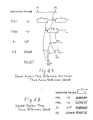
- motor 10 rotates at reference speed (Fig. 2); motor 10 rotates at a speed which is lower than the reference speed (Fig. 3); motor 10 rotates at a speed higher than the reference speed but less than twice the reference speed (Fig. 4A); motor 10 rotates at a speed higher than twice reference speed (Fig. 4B).
- Fig.2 Operation of the System of Fig. 1 at Reference Speed of Motor
- An indicator pulse P1 from encoder 12 triggers timer TM1 to initiate timed interval T1.
- the negative output O of timer TM1 triggers timer TM2 and flip-flop F3.
- the output of flip-flop F3 resets flip-flops F1, F2, and F3 via gate G2. This action prepares flip-flops F1 and F2 for period comparison between the next indicator pulse signal (P2) and termination of period T2 of the negative output O of TM2.
- signal P2 arrives at the clock input of flip-flop F2 in synchronism with the trailing edge of the output signal of timer TM2 at the clock input of F1.
- both flip-flops are set at the same time and then are reset via gates G1 and G2.
- the duration of UP and DOWN signals is the same and depends on the propagation delay of G1 and G2 and the reset times of flip-flops F1 and F2.
- Fig. 3 Operation of the System of Fig. 1 at Motor Speed Lower than Reference Speed
- the difference in lengths of the UP and DOWN signals of F1 and F2 is equal to the error time t(e). Because the width of the UP signal exceeds that of the DOWN signal, the voltage on integrator 19 will increase in proportion to the period error, thereby causing motor 10 to accelerate.
- Fig. 4B Operation of System of Fig. 1 at Motor Speed Higher Than Twice Reference Speed
- indicator pulses when the motor is at a speed higher than twice reference speed, indicator pulses have a period T(IND) which is less than T1. Therefore, timer TM1 is restarted by indicator pulses before terminal count can occur, so the negative output O of timer TM1 is always low. As a result, timer TM2 is never triggered and negative output O of timer TM2 is always high. Also, flip-flop F3 is never triggered, so the usual RS2 reset does not occur. Then the only triggering input at period comparator 16 is a string of indicator pulses applied to the clock input of flip-flop F2.
- Fig. 5 Charge Pump with Integrator
- Charge pump 100 comprises an inverter 110 and a non-inverter (buffer or isolator) 112.
- the outputs of elements 110 and 112 have two levels, i.e., zero and +V.
- the inputs of gates 110 and 112 are connected to respective outputs O(UP) and O(DOWN) of period comparator 16 (Fig. 1).
- the output of gate 110 is coupled to the input of integrator 200 via a series circuit consisting of a diode 116 and a resistor 118, while the output of gate 112 is coupled to the same input via diode 120 and resistor 122.
- Diodes 116 and 120 are oppositely polarized.
- Integrator 200 consists of an operational amplifier which comprises a high-gain amplifier 114 which has a positive input terminal biased to +V/2.
- the other (i.e., negative) input of amplifier 114 has its voltage approximately equal to that of the positive input, i.e., in this case +V/2.
- Output L of amplifier 114 is connected to its negative input by means of a capacitive feedback network 124, which is similar to that of integrator 19.
- Corresponding elements are designated by the same reference numerals but with addition of suffix "b".
- Charge pump 100 operates with integrator 200 as follows: When the O(UP) signal is low, the output of inverting gate 110 is +V, and neglecting voltage drop across diode 116, a voltage of +V/2 is impressed across resistor 118. This produces a proportional current. On the other hand, when output of gate 110 is at high level, diode 116 is back biased, so no current flows.
- FIG. 6 Another embodiment of a unit composed of a charge pump 300 with an integrator 400 is shown in Fig. 6.
- This embomodification differs from the previous one in that MOS transistors 130 and 132 are used instead of diodes 116 and 120 of Fig. 5.
- the input O(DOWN) is applied to an inverting gate 134
- the input O(UP) is applied to non-inverting gate 136. This is done to provide consistency with the earlier circuits where output L is positive going for UP commands.
- An advantage of this circuit as compared to one using diodes (Fig. 5) is that the MOS transistors connect resistors 138 and 140 to +V or to ground, respectively, without the voltage drop inherent in diodes.
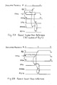
- Figs. 7, 8A, and 8B Control Circuit Using Period Generator with Single Timer (Figs. 7, 8A and 8B)
- Fig. 7 shows a timing diagram illustrating operation of the system of Fig. 7 at a speed which is higher than reference speed and Fig. 8B shows a timing diagram of the same in case where the motor speed is lower than the reference speed.
- the motor speed control system shown in Fig. 7 consists of a motor 10a, an electromechanical encoder 12a, and a pulse generator circuit 14a which is formed using one timer TMa.
- the system also has a flip-flop Fa which has an input C, an input D, and output Q and a negative output Q.
- Encoder 12a is connected to input C of flip-flop Fa.
- the negative output Q of flip-flop Fa is connected to input D of flip-flop Fa and to input G of timer TMa.
- Clock C of counter TMa is attached to a crystal-controlled oscillator XTALa OSC.
- the system has three flip-flops (F1a, F2a, and F3a with respective inputs and outputs) and logic elements (an AND gate G1a and an OR gate G2a with respective inputs and outputs).
- a negative output O of timer TMa is connected to input C of flip-flop F1a, an output Q of flip-flop Fa is connected to an input C of flip-flop F2a, and a negative output Q of flip-flop Fa is connected to an input C of flip-flop F3a.
- the timers can be implemented as counters, one-shots (monostable multivibrators), or other parts suitable for that purpose.
- the system shows one or two timers but it can be implemented with more than two timers in conjunction with other circuits. Although in the description equal values are used for T1 and T2, this is not necessary. The assumption of equality is made for ease of description only.
- the system of the invention has been illustrated in application to control of a motor. This motor was shown as a brushless DC motor. It can be, however, any other kind of motor suitable for the purpose. It should be understood, also, that this system is equally applicable to voltage-controlled oscillators or pattern generators. Thus, the scope of the invention should be determined, not by the examples given, but by appended claims and their legal equivalents.
Abstract
Description
- The present invention relates to motor speed control systems and analogs thereof, particularly to a control system for maintaining the speed of the motor constant with a high degree of accuracy.
- Precision motor speed control circuits have a variety of applications, including phonographic turntables, audio or video tape recorders, and disk drive units.
- One circuit for accurately controlling the speed of a motor is disclosed in U.S. Patent No. 4,516,060 to N. Guzik and G. Mangeym, May 7, 1985. Although this circuit can provide accuracy within 0.1% of the desired speed, it still entails some problems. Specifically, since the integrator of the system uses capacitors which work in a charge/discharge mode, the accuracy of the speed control circuit depends essentially on the accuracy of the capacitors and the circuit's other components. In addition, the control voltages from the integrator have a sawtooth shape; this causes undesirable ripple in the motor's current.
- Accordingly, an object of the present invention is to reduce dependence of system's performance on accuracy of the circuit's components. Other objects are to improve accuracy of a motor speed control system to about 0.01%, and to provide a novel sample and hold function and to eliminate motor current ripple. Further objects and advantages will become apparent from a consideration of the ensuing description and drawings.
-
- Figure 1 is a block diagram of a motor speed control system of the invention.
- Figure 2 is a timing diagram illustrating operation of the system of Fig. 1 when the motor is turning at a reference speed.
- Figure 3 is a timing diagram illustrating operation of the system of Fig. 1 when the motor's speed is lower than the reference speed.
- Figure 4A is a timing diagram illustrating operation of the system of Fig. 1 when the motor's speed is higher than reference speed but lower than twice reference speed.
- Figure 4B is a timing diagram illustrating operation of the system of Fig. 1 when the motor's speed is higher than twice reference speed.
- Figure 5 is a diagram illustrating a specific embodiment of a charge pump and integrator of the circuit of Fig. 1.
- Figure 6 is a schematic circuit diagram illustrating another embodiment of the charge pump.
- Figure 7 is a diagram of the motor speed control circuit using a period comparator with only one counter.
- Figure 8A is a timing diagram illustrating operation of the system of Fig. 7 in the case where the speed of the motor is higher than reference speed.
- Figure 8B is a timing diagram similar to that of Fig. 8A, except that the motor's speed is lower than reference speed.
- A motor speed control system shown in Fig. 1 consists of a d.c. motor 10, an electromechanical encoder 12 (which can be a mechanical, optoelectric, magnetic or any other pulse-generating encoder), and a
reference generator circuit 14 which is formed of two counters TM1 and TM2 which in this particular embodiment operate as timers, and aperiod comparator 16, acharge pump 18, anintegrator 19, and apower driver 20.Encoder 12 generates one or more speed indicating pulses for each revolution of the motor; thus the frequency of these indicator pulses is in proportion to the motor's rotational speed. - Timers TM1 and TM2 are known per se and comprise, e.g., 8254 type programmable interval timers produced by Intel Corp. The 8254 counter timer is commonly used in computer control systems and can be adapted to a variety of tasks by selection of one of several possible modes of operation. Inputs for data, write enable, and chip select (not shown in the drawings) are provided; these inputs for both timers (TM1 and TM2) are connected to an external computer bus or any other suitable source (not shown) so that the counter timers can be initialized. In this case, each counter timer is set to operate as a "hardware retriggerable one-shot", as described in the "Intel Microprocessor and Peripheral Handbook", 1983.
- Each timer has a clock input C connected to a crystal-controlled oscillator (XTAL OSC) 15. Also each timer has a gate input G. A positive-going input at G starts the timing period T running. An internal count value, previously set during initialization, is determined by each clock pulse, until a count of zero terminates the timing period. By this means, an output pulse O (not shown in the drawings) is generated having a controlled pulse length T with an accuracy equal to that of a
XTAL OSC 15. Timers TM1 and TM2 generate timing pulses having durations T1 and T2 respectively. Each timer's output includes a circle or "bubble", indicating that each timer's output is inverted; this causes the leading edges of the timing periods to be negative going, and the trailing edges to be positive going as shown. - It was previously stated that the timers are retriggerable. This means that if new triggering occurs before termination of a timer output, then the timer output is extended. Termination of the output pulse takes place at time T following occurance of the latest triggering signal.
- The trailing edges of the timers' outputs are supplied to a
period comparator 16 which consists of two D-type flip-flops F1 and F2, an AND gate G1, an inclusive OR gate G2 and a third D-type flip-flop F3. The output of timer TM2 is connected to a clock input C of flip-flop F1. The clock input C of flip-flop F2 is connected to the output ofencoder 12. The D inputs of flip-flops F1, F2, and F3 receive constant ONE signals. - The Q outputs of flip-flops F1 and F2, which supply UP and DOWN signals, respectively, are coupled through series-connected gates G1 and G2 to reset inputs R of flip-flops F1, F2, and F3, respectively.
- For convenience of description, we will refer to the output of gate G1 as reset RS1, and the output of flip-flop F3 as reset RS2; resets RS1 and RS2 are supplied to OR gate G2. The output of timer TM1 is connected to the clock input of flip-flop F3 and the output of flip-flop F3 is connected to the other input of OR gate G2.
- The system is provided with a START input line which is connected to the set input S of flip-flop F1. This line receives an initiating pulse from an external source such as a computer or the like (not shown in the drawings).
-
Period comparator 16 is connected to acharge pump 18 which functionally is shown to consist of two current sources I(up) and I(down) in series with logic-controlled switch units SW1 and SW2. The switch units operate so that current flow to a common point C may be enabled or disabled in response to control inputs O(up) and O(down) fromperiod comparator 16. More specific embodiments of the charge pump will be described later in connection with Figs. 5 and 6. - The common point C of the switched current sources is connected to an
integrator 19 which consists of resistor R1 and capacitor C1 which are connected in series from point C to ground and which are shunted by capacitor C2. Normally C1 is the dominant component ofintegrator 19, and the voltage at point C is closely approximated by the inverse of the magnitude of C1 multiplied by the accumulated charge at point C, i.e., the voltage is proportional to the time integral of input current I(up) - I(down). - Components R1 and C2 modify the behavior of the integrator, more particularly at upper frequency limits of the speed control system. They are used to stabilize the speed control system by "lead-lag compensation", a procedure that is well known to control system engineers.
-
Charge pump 18 andintegrator 19 function as a digital-to-analog converter. - The output of
integrator 19 is input to a voltage-controlledpower driver 20, which, in turn, closes the control loop to motor 10. An example of a suitable power driver for use with a brushless three-phase DC motor, is type TA 7259P integrated curcuit manufactured by Toshiba Corporation. The manner of use of this circuit with such a motor is described in Toshiba "Motor Control and Driver IC Series Data Book", 1984. - In the context of the present invention, "UP" means that the speed of the motor is to be increased and "DOWN" means that slow down of the motor is desired.
- Initially, because the motor is at rest, there are no speed indicator pulses from
encoder 12 to operatepulse comparator 16. Therefore to begin operation, a START pulse is first applied to the set input S of flip-flop F1, causing it to be placed in the UP condition. Because UP can be cancelled by DOWN, we must also examine the condition of flip-flop F2. If flip-flop F2 is initially in the DOWN state, i.e., its Q output is high, then both inputs of AND gate G1 are high. Output RS1 of gate G1 will be high, causing the output of OR gate G2 to be high, in turn applying a reset pulse to all three flip-flops F1, F2, and F3. Because of the presence of the START pulse at set input S of flip-flop F1, the UP condition is retained, but flip-flops F2 and F3 are both reset. As a result, an UP signal alone will be supplied to chargepump 18, which will in turn supply an UP signal tointegrator 19. The integrator will supply an output topower driver 20 which will in turn cause motor 10 to rotate. - Instead of continuing with description of acceleration of the motor from its starting condition, the essence of the invention will be easier understood if we assume that the motor is already at operating speed. Each of the following conditions will be considered separately: motor 10 rotates at reference speed (Fig. 2); motor 10 rotates at a speed which is lower than the reference speed (Fig. 3); motor 10 rotates at a speed higher than the reference speed but less than twice the reference speed (Fig. 4A); motor 10 rotates at a speed higher than twice reference speed (Fig. 4B).
- This is an ideal case. As shown in Fig. 2, when the motor is at reference speed, the period T(IND) between indicator pulses P1 and P2 is exactly equal to a reference value generated by the sum of time periods T1 and T2 of the pulses generated by timers TM1 and TM2. That is, the following condition exists:
T(IND) = T1 + T2. - An indicator pulse P1 from
encoder 12 triggers timer TM1 to initiate timed interval T1. - At the end of period T1, the negative output O of timer TM1 triggers timer TM2 and flip-flop F3. The output of flip-flop F3 resets flip-flops F1, F2, and F3 via gate G2. This action prepares flip-flops F1 and F2 for period comparison between the next indicator pulse signal (P2) and termination of period T2 of the negative output O of TM2.
- In the case under consideration, signal P2 arrives at the clock input of flip-flop F2 in synchronism with the trailing edge of the output signal of timer TM2 at the clock input of F1. As a result, both flip-flops are set at the same time and then are reset via gates G1 and G2. The duration of UP and DOWN signals is the same and depends on the propagation delay of G1 and G2 and the reset times of flip-flops F1 and F2.
- As a result, the UP and DOWN signals cancel each other, so that the INPUT and OUTPUT voltages of
inregrator 19 are not changed, whereby rotation speed is left unchanged. - As shown in Fig. 3, when the motor is at a speed lower than reference speed, the trailing edge of the negative output O (not shown in the drawings) of timer TM2 sets flip-flop F1 in an UP condition. Next, indicator pulse P2 arrives after a period error t(e) equal to the difference between reference and indicator pulse periods. Pulse P2 triggers flip-flop F2, setting
comparator 16 in the DOWN state. As has been described earlier, when UP and DOWN exist together, then via AND gate G1 and OR gate G2, flip-flops F1 and F2 receive a reset pulse. This will cause both UP and DOWN flip-flops F1 and F2 to be reset via gates G1 and G2. As shown in Fig. 3, the difference in lengths of the UP and DOWN signals of F1 and F2 is equal to the error time t(e). Because the width of the UP signal exceeds that of the DOWN signal, the voltage onintegrator 19 will increase in proportion to the period error, thereby causing motor 10 to accelerate. - As shown in Fig. 4A, when the motor is at a speed higher than reference speed but less than twice reference speed, at the end of period T1, negative output O of timer TM1 triggers timer TM2 and flip-flop F3 (Fig. 1). The output of flip-flop F3 resets flip-flops F1, F2, and F3 via gate G2. This action prepares flip-flops F1 an F2 for comparison of the period between the next indicator pulse signal (P2) and the trailing edge of the output signal of TM2. In the case under consideration, signal P2 arrives at the clock input of flip-flop F2 before the trailing edge of the negative output signal O of timer TM2 at the clock input of F1. Therefore, the DOWN signal occurs first and is longer than the UP signal by the period error t(e). As a result, the motor's speed will decelerate.
- As shown in Fig. 4B, when the motor is at a speed higher than twice reference speed, indicator pulses have a period T(IND) which is less than T1. Therefore, timer TM1 is restarted by indicator pulses before terminal count can occur, so the negative output O of timer TM1 is always low. As a result, timer TM2 is never triggered and negative output O of timer TM2 is always high. Also, flip-flop F3 is never triggered, so the usual RS2 reset does not occur. Then the only triggering input at
period comparator 16 is a string of indicator pulses applied to the clock input of flip-flop F2. If an UP condition had initially been present at flip-flop F1, it would be reset via gates G1 and G2 by a triggered DOWN condition at F2. Therefore, only the DOWN condition is retained, and this decelerates motor 10. When speed has fallen to less than twice the reference speed, the condition of the earlier described Mode I occurs. - A specific embodiment of a
charge pump 100 with anintegrator 200 is shown in Fig. 5.Charge pump 100 comprises aninverter 110 and a non-inverter (buffer or isolator) 112. The outputs ofelements gates gate 110 is coupled to the input ofintegrator 200 via a series circuit consisting of adiode 116 and aresistor 118, while the output ofgate 112 is coupled to the same input viadiode 120 andresistor 122.Diodes -
Integrator 200 consists of an operational amplifier which comprises a high-gain amplifier 114 which has a positive input terminal biased to +V/2. As is well known in the art, the other (i.e., negative) input ofamplifier 114 has its voltage approximately equal to that of the positive input, i.e., in this case +V/2. Output L ofamplifier 114 is connected to its negative input by means of acapacitive feedback network 124, which is similar to that ofintegrator 19. Corresponding elements are designated by the same reference numerals but with addition of suffix "b". -
Charge pump 100 operates withintegrator 200 as follows: When the O(UP) signal is low, the output of invertinggate 110 is +V, and neglecting voltage drop acrossdiode 116, a voltage of +V/2 is impressed acrossresistor 118. This produces a proportional current. On the other hand, when output ofgate 110 is at high level,diode 116 is back biased, so no current flows. - Therefore, when the O(UP) signal is pulsed high, a charge is pumped out of the negative terminal of
integrator 200 in proportion to the above-mentioned current and the pulse time.Gate 112, in conjunction withdiode 120 andresistor 122 operates in a similar manner except that current and charge slow in the reverse direction, i.e., into the negative terminal ofintegrator 200. Thus, it can be understood that depending on UP or DOWN conditions on the inputs to chargepump 100, the charge flows either from or tointegrator 200.Integrator 200 integrates the charge in a manner similar to that which has been described with reference tointegrator 19. However, the integrator voltage is developed acrossintegrator network 124 to produce an output at L(b). This output is positive for generally UP condition, and negative for generally DOWN condition, as for the earlier described charge pump and integrator (Fig. 1). - Another embodiment of a unit composed of a
charge pump 300 with anintegrator 400 is shown in Fig. 6. This embomodification differs from the previous one in thatMOS transistors diodes gate 134, whereas the input O(UP) is applied tonon-inverting gate 136. This is done to provide consistency with the earlier circuits where output L is positive going for UP commands. An advantage of this circuit as compared to one using diodes (Fig. 5) is that the MOS transistors connectresistors - The embodiments described above were based on a period generator using two counters. However, the invention also can be realized by means of a control circuit having only one counter which also works as a timer. The embodiment with one timer is illustrated in Fig.7. Fig. 8A shows a timing diagram illustrating operation of the system of Fig. 7 at a speed which is higher than reference speed and Fig. 8B shows a timing diagram of the same in case where the motor speed is lower than the reference speed.
- Since the system of this embodiment is generally identical to that described above, only different parts of it will be described. Where parts in the second embodiment are similar to those of Fig.1, they are designated by the same reference numerals with addition of suffix "a".
- The motor speed control system shown in Fig. 7 consists of a
motor 10a, an electromechanical encoder 12a, and apulse generator circuit 14a which is formed using one timer TMa. The system also has a flip-flop Fa which has an input C, an input D, and output Q and a negative output Q. Encoder 12a is connected to input C of flip-flop Fa. The negative output Q of flip-flop Fa is connected to input D of flip-flop Fa and to input G of timer TMa. Clock C of counter TMa is attached to a crystal-controlled oscillator XTALa OSC. - Similar to the circuit of the first embodiment, the system has three flip-flops (F1a, F2a, and F3a with respective inputs and outputs) and logic elements (an AND gate G1a and an OR gate G2a with respective inputs and outputs).
- A negative output O of timer TMa is connected to input C of flip-flop F1a, an output Q of flip-flop Fa is connected to an input C of flip-flop F2a, and a negative output Q of flip-flop Fa is connected to an input C of flip-flop F3a.
- Operation of the system of Fig. 7 is very similar to that described with regard to Fig. 1 and its respective timing diagrams for high and low speed. However, there is only one timer in the circuit. Therefore only every second indicator pulse results in a period comparison. Based on the previous detailed description, those skilled in the art can easily understand the principle and sequence of operations of the circuit of Fig. 7 by referring to the timing diagrams shown in Figs. 8A and 8B for high and low speeds, respectively.
- Since only every other indicator pulse results in a period sample, some decrease in the accuracy of speed control can result if there is significant second harmonic distortion in the indicator pulse signal. In addition, the sampling rate is halved.
- Thus, in operation of the above-described system, when no correction to speed is required, no net charge is pumped, and the integrator "holds" the previous condition of motor drive operation. On the other hand, if motor speed is incorrect, the error condition is sampled through the control circuit and the speed is corrected by modifying the charge on the integrator. As compared to the control circuit of the aforementioned US Patent 4,516,060, the sample and hold mode of operation of the control circuit generally has a constant output at the integrator and therefore does not introduce any ripple on the motor current. In addition, the accuracy of control is improved since the control circuit compares indicator period T(IND), which is itself an integral submultiple of the motor's rotation period, to a reference period T1 + T2, which is an integral multiple of the crystal-controlled clock period. Any difference between the compared indicator and reference periods causes charge to flow into the integrator circuit, thus modifying the motor's speed until T(IND) = T1 + T2. This condition occurs irrespective of inaccuracies in components of the circuits used. Thus motor speed has substantially the same accuracy as that of the crystal clock. Although the present invention has been described and shown with reference to specific circuits and circuit components, those skilled in the art understand that many other modifications of the speed control circuit are possible. For example, the timers can be implemented as counters, one-shots (monostable multivibrators), or other parts suitable for that purpose. The system shows one or two timers but it can be implemented with more than two timers in conjunction with other circuits. Although in the description equal values are used for T1 and T2, this is not necessary. The assumption of equality is made for ease of description only. The system of the invention has been illustrated in application to control of a motor. This motor was shown as a brushless DC motor. It can be, however, any other kind of motor suitable for the purpose. It should be understood, also, that this system is equally applicable to voltage-controlled oscillators or pattern generators. Thus, the scope of the invention should be determined, not by the examples given, but by appended claims and their legal equivalents.
Claims (12)
a motor;
encoding means connected to said motor for generating indicator pulses related to rotational speed of said motor;
period generator means comprising at least one counter which is initiated by said encoder means and generates a reference pulse period;
a period comparator connected to said encoder means and to said period generator means, said period comparator having means for comparing said reference period to a period of said indicator pulses of said encoder and for producing an output signal as a result of the comparison, said period comparator having resetting means which resets said period comparator in response to said output signal;
digital-to-analog converter means having an input and an output, said period comparator being connected to said input of said converter means; and
motor driver means responsive to the output signal of said converter means for controlling the speed of said motor, said driver means having an input and an output, said output of said driver means being connected to said motor.
a motor;
encoding means connected to said motor for generating a succession of indicator pulses related to the speed of said motor;
timer means comprising a counter having clock, gate inputs and an output, clock generator means connected to said clock input of said counter;
a first flip-flop, a second flip-flop, and a third flip-flop, each of said flip-flops having a triggering input, a reset input, and an output, an AND gate element and an OR gate each having two inputs and one output, said output of said counter being connected to said clock input of said first flip-flop, said output of said first flip-flop being connected to a first input of said AND gate, said output of said second flip-flop being connected to a second input of said AND gate, said output of said AND gate being connected to a first input of said OR gate, said output of said third flip-flop being connected to a second input of said OR gate, said output of said OR gate being connected to said reset inputs of said first, second and third flip-flops, a fourth flip-flop having a triggering input, a data input, a non-inverted output and an inverted output, said encoder means being connected to said triggering input of said fourth flip-flop, said inverted output of said fourth flip-flop being connected to said data input, to said gate input of said counter, and to said triggering input of said third flip-flop, said non-inverted output of said fourth flip-flop being connected to said triggering input of said second flip-flop;
charge pump means consisting of first and second switchable current sources having inputs and outputs, said input of said first switchable current source being connected to said output of said first flip-flop and said input of said second switchable current source being connected to said output of said second flip-flop, the outputs of said switchable current sources being connected to each other and forming a common output from said charge pump means;
integrator means having an input and an output; and
a power driver means having input and output, said input of said integrator means being connected to said output of said charge pump means, said output of said integrator means being connected to said input of said power driver, said output of said power driver being connected to said motor.
a motor;
encoding means connected to said motor for generating a succession of indicator pulses related to the speed of said motor;
timer means consisting of a first counter and a second counter, each counter having a clock input, a gate input, and an output, a clock generator means connected to said clock inputs of both said counters, the output of said first counter being connected to the gate input of said second counter;
a period comparator comprising a first flip-flop, a second flip-flop, and a third flip-flop, each of said flip-flops having a triggering input, a reset input, and an output, said output of said first counter being connected to the triggering input of said third flip-flop, said output of said second counter being connected to the triggering input of said first flip-flop, said encoding means being connected to said gate input of said first timer and to said triggering input of said second flip-flop, an AND gate and an OR gate, each having two inputs and one output, said output of said first flip-flop being connected to one input of said AND gate and said output of said second flip-flop being connected to the second input of said AND gate, said output of said AND gate being connected to one input of said OR gate, the second input of said OR gate being connected to the output of said third flip-flop, the output of said OR gate being connected to the reset inputs of all said flip-flops;
charge pump means consisting of first and second switchable current sources having inputs and outputs, said input of said first switchable current source being connected to said output of said first flip-flop and said input of said second switchable current source being connected to said output of said second flip-flop, the outputs of said switchable current sources being connected to each other and forming a common output from said charge pump means;
integrator means having an input and an output; and a power driver means having an input and an output, said input of said integrator means being connected to said output of said charge pump means, said output of said integrator means being connected to said input of said power driver, said output of said power driver being connected to said motor.
Applications Claiming Priority (2)
| Application Number | Priority Date | Filing Date | Title |
|---|---|---|---|
| US868735 | 1986-05-30 | ||
| US06/868,735 US4680516A (en) | 1986-05-30 | 1986-05-30 | Motor speed control system |
Publications (2)
| Publication Number | Publication Date |
|---|---|
| EP0247624A2 true EP0247624A2 (en) | 1987-12-02 |
| EP0247624A3 EP0247624A3 (en) | 1989-10-04 |
Family
ID=25352235
Family Applications (1)
| Application Number | Title | Priority Date | Filing Date |
|---|---|---|---|
| EP87107826A Withdrawn EP0247624A3 (en) | 1986-05-30 | 1987-05-29 | Motor speed control system |
Country Status (3)
| Country | Link |
|---|---|
| US (1) | US4680516A (en) |
| EP (1) | EP0247624A3 (en) |
| JP (1) | JPS63121483A (en) |
Cited By (2)
| Publication number | Priority date | Publication date | Assignee | Title |
|---|---|---|---|---|
| EP0345556A1 (en) * | 1988-05-26 | 1989-12-13 | Fujitsu Limited | Counter circuitry for motor rotation speed control circuitry |
| EP0744822A2 (en) * | 1995-05-22 | 1996-11-27 | Canon Kabushiki Kaisha | Motor rotational speed control apparatus |
Families Citing this family (15)
| Publication number | Priority date | Publication date | Assignee | Title |
|---|---|---|---|---|
| DE3609566A1 (en) * | 1986-03-21 | 1987-10-08 | Pfaff Haushaltmasch | SPEED CONTROL OF AN ELECTRIC MOTOR |
| EP0239655A1 (en) * | 1986-04-01 | 1987-10-07 | Océ-Nederland B.V. | Electronic proportional-integral-controller in digital execution |
| USRE33500E (en) * | 1986-04-01 | 1990-12-18 | Oce-Nederland B.V. | Electronic digitized proportional-integral controller |
| JP2523609B2 (en) * | 1987-03-31 | 1996-08-14 | 株式会社東芝 | Motor speed controller |
| JPS63159932U (en) * | 1987-04-09 | 1988-10-19 | ||
| US4823055A (en) * | 1987-12-21 | 1989-04-18 | Superdrive Systems, Inc. | Electronic control circuit for command systems |
| JP3136321B2 (en) * | 1991-07-15 | 2001-02-19 | ローム株式会社 | Motor control circuit and motor control device |
| US5517379A (en) * | 1993-05-26 | 1996-05-14 | Siliconix Incorporated | Reverse battery protection device containing power MOSFET |
| US5539610A (en) * | 1993-05-26 | 1996-07-23 | Siliconix Incorporated | Floating drive technique for reverse battery protection |
| US5825972A (en) * | 1995-02-17 | 1998-10-20 | Dell Usa, L.P. | Direct current fan motor speed controller |
| US5640071A (en) * | 1995-10-10 | 1997-06-17 | Malaspina; Francis P. | Transient charge recovery circuit |
| US5930736A (en) * | 1997-01-21 | 1999-07-27 | Dell Usa, L.P. | Fan monitoring system |
| JP3700325B2 (en) * | 1997-05-21 | 2005-09-28 | 松下電器産業株式会社 | Drive source control method |
| KR100434236B1 (en) * | 2001-10-11 | 2004-06-04 | 페어차일드코리아반도체 주식회사 | A motor control driving circuit |
| US7215091B2 (en) * | 2003-01-03 | 2007-05-08 | Lexmark International, Inc. | Method for controlling a DC printer motor with a motor driver |
Citations (4)
| Publication number | Priority date | Publication date | Assignee | Title |
|---|---|---|---|---|
| US3950682A (en) * | 1974-12-19 | 1976-04-13 | International Business Machines Corporation | Digital dc motor velocity control system |
| US4052676A (en) * | 1976-06-10 | 1977-10-04 | Woodward Governor Company | Digital-analog frequency error signaling |
| US4376262A (en) * | 1980-02-29 | 1983-03-08 | Fuji Electrochemical Co., Ltd. | Method and apparatus for controlling a digital controlled brushless motor |
| US4516060A (en) * | 1982-11-19 | 1985-05-07 | Nahum Guzik | Digital motor speed control |
Family Cites Families (5)
| Publication number | Priority date | Publication date | Assignee | Title |
|---|---|---|---|---|
| US3564368A (en) * | 1968-01-10 | 1971-02-16 | Gen Electric | Spindle speed control monitor |
| US4153863A (en) * | 1977-04-20 | 1979-05-08 | Colt Industries Operating Corp. (Pratt & Whitney Machine Tool Division) | DC Motor controller |
| US4463300A (en) * | 1981-09-17 | 1984-07-31 | Printronix, Inc. | Linear motor digital servo control |
| JPS5854885A (en) * | 1981-09-25 | 1983-03-31 | Sony Corp | Control circuit for direct current motor |
| NL8502479A (en) * | 1985-09-11 | 1987-04-01 | Philips Nv | SYSTEM FOR CONTROLLING THE SPEED OF AN ELECTRIC MOTOR. |
-
1986
- 1986-05-30 US US06/868,735 patent/US4680516A/en not_active Expired - Lifetime
-
1987
- 1987-05-27 JP JP62128543A patent/JPS63121483A/en active Pending
- 1987-05-29 EP EP87107826A patent/EP0247624A3/en not_active Withdrawn
Patent Citations (4)
| Publication number | Priority date | Publication date | Assignee | Title |
|---|---|---|---|---|
| US3950682A (en) * | 1974-12-19 | 1976-04-13 | International Business Machines Corporation | Digital dc motor velocity control system |
| US4052676A (en) * | 1976-06-10 | 1977-10-04 | Woodward Governor Company | Digital-analog frequency error signaling |
| US4376262A (en) * | 1980-02-29 | 1983-03-08 | Fuji Electrochemical Co., Ltd. | Method and apparatus for controlling a digital controlled brushless motor |
| US4516060A (en) * | 1982-11-19 | 1985-05-07 | Nahum Guzik | Digital motor speed control |
Cited By (6)
| Publication number | Priority date | Publication date | Assignee | Title |
|---|---|---|---|---|
| EP0345556A1 (en) * | 1988-05-26 | 1989-12-13 | Fujitsu Limited | Counter circuitry for motor rotation speed control circuitry |
| US5058191A (en) * | 1988-05-26 | 1991-10-15 | Fujitsu Limited | Motor rotation speed control circuit |
| EP0744822A2 (en) * | 1995-05-22 | 1996-11-27 | Canon Kabushiki Kaisha | Motor rotational speed control apparatus |
| EP0744822A3 (en) * | 1995-05-22 | 1998-01-14 | Canon Kabushiki Kaisha | Motor rotational speed control apparatus |
| US5808431A (en) * | 1995-05-22 | 1998-09-15 | Canon Kabushiki Kaisha | Motor rotational speed control apparatus |
| CN1047042C (en) * | 1995-05-22 | 1999-12-01 | 佳能株式会社 | Motor rotational speed control apparatus |
Also Published As
| Publication number | Publication date |
|---|---|
| EP0247624A3 (en) | 1989-10-04 |
| US4680516A (en) | 1987-07-14 |
| JPS63121483A (en) | 1988-05-25 |
Similar Documents
| Publication | Publication Date | Title |
|---|---|---|
| US4680516A (en) | Motor speed control system | |
| US4271382A (en) | Speed control circuit for phase-locked loop motor drive systems | |
| US3986125A (en) | Phase detector having a 360 linear range for periodic and aperiodic input pulse streams | |
| JPS61288789A (en) | Phase lock loop unit | |
| US4376914A (en) | Motor control device | |
| US4516060A (en) | Digital motor speed control | |
| US5293445A (en) | AGC with non-linear gain for PLL circuits | |
| US3424966A (en) | Synchronous servo loop control system | |
| JPH11178380A (en) | Motor speed controller | |
| JPS648541B2 (en) | ||
| JPS6310668B2 (en) | ||
| US4739237A (en) | PLL motor controller | |
| US4495460A (en) | Resettable feedback sensor | |
| JPH087837Y2 (en) | Motor control device | |
| JPH0817583B2 (en) | Speed servo circuit | |
| JPH0811069Y2 (en) | Motor control device | |
| KR910000957Y1 (en) | Frequency comparateing circuit | |
| JPS5912218B2 (en) | variable frequency oscillation circuit | |
| SU1644085A1 (en) | Regulator of speed of rotation of dc motor | |
| JP2584435B2 (en) | Speed servo circuit | |
| JPS5927195B2 (en) | Commutatorless motor | |
| JPS6198176A (en) | Motor controller | |
| JPS6035983A (en) | Controller of motor | |
| JPH0514514B2 (en) | ||
| JPS5839292A (en) | Digital system motor speed control circuit |
Legal Events
| Date | Code | Title | Description |
|---|---|---|---|
| PUAI | Public reference made under article 153(3) epc to a published international application that has entered the european phase |
Free format text: ORIGINAL CODE: 0009012 |
|
| AK | Designated contracting states |
Kind code of ref document: A2 Designated state(s): DE FR GB IT |
|
| PUAL | Search report despatched |
Free format text: ORIGINAL CODE: 0009013 |
|
| AK | Designated contracting states |
Kind code of ref document: A3 Designated state(s): DE FR GB IT |
|
| 17P | Request for examination filed |
Effective date: 19891205 |
|
| 17Q | First examination report despatched |
Effective date: 19920710 |
|
| STAA | Information on the status of an ep patent application or granted ep patent |
Free format text: STATUS: THE APPLICATION IS DEEMED TO BE WITHDRAWN |
|
| 18D | Application deemed to be withdrawn |
Effective date: 19921121 |
|
| RIN1 | Information on inventor provided before grant (corrected) |
Inventor name: GUZIK, NAHUM Inventor name: MANGEYM, GENNADY Inventor name: JONES, JAMES W. |