EP0093430A2 - Pipeline data processing system - Google Patents
Pipeline data processing system Download PDFInfo
- Publication number
- EP0093430A2 EP0093430A2 EP83104228A EP83104228A EP0093430A2 EP 0093430 A2 EP0093430 A2 EP 0093430A2 EP 83104228 A EP83104228 A EP 83104228A EP 83104228 A EP83104228 A EP 83104228A EP 0093430 A2 EP0093430 A2 EP 0093430A2
- Authority
- EP
- European Patent Office
- Prior art keywords
- instruction
- register
- instructions
- line
- result
- Prior art date
- Legal status (The legal status is an assumption and is not a legal conclusion. Google has not performed a legal analysis and makes no representation as to the accuracy of the status listed.)
- Granted
Links
Images


Classifications
-
- G—PHYSICS
- G06—COMPUTING; CALCULATING OR COUNTING
- G06F—ELECTRIC DIGITAL DATA PROCESSING
- G06F9/00—Arrangements for program control, e.g. control units
- G06F9/06—Arrangements for program control, e.g. control units using stored programs, i.e. using an internal store of processing equipment to receive or retain programs
- G06F9/30—Arrangements for executing machine instructions, e.g. instruction decode
- G06F9/38—Concurrent instruction execution, e.g. pipeline, look ahead
- G06F9/3885—Concurrent instruction execution, e.g. pipeline, look ahead using a plurality of independent parallel functional units
- G06F9/3889—Concurrent instruction execution, e.g. pipeline, look ahead using a plurality of independent parallel functional units controlled by multiple instructions, e.g. MIMD, decoupled access or execute
-
- G—PHYSICS
- G06—COMPUTING; CALCULATING OR COUNTING
- G06F—ELECTRIC DIGITAL DATA PROCESSING
- G06F9/00—Arrangements for program control, e.g. control units
- G06F9/06—Arrangements for program control, e.g. control units using stored programs, i.e. using an internal store of processing equipment to receive or retain programs
- G06F9/30—Arrangements for executing machine instructions, e.g. instruction decode
- G06F9/38—Concurrent instruction execution, e.g. pipeline, look ahead
- G06F9/3824—Operand accessing
- G06F9/383—Operand prefetching
Definitions
- the present invention relates to a pipelined data processing system, and more particularly to a pipelined data processing system in which an instruction is executed in a plurality of stages each having an independent hardware and the stages are operated in an overlapped mode.
- an instruction is executed in five to seven stages with each stage being operated in one machine cycle (basic cycle of the data processing system) and the stages being operated in an overlapped mode so that each instruction is apparently executed in one cycle.
- an instruction is processed in five stages, that is, a D-stage in which the instruction is decoded and an operand address is determined by adding a content of a general purpose register designated by an index field of the instruction, a content of a general purpose register designated by a base field of the instruction and a content of a displacement field of the instruction; an A-stage in which the logical operation address determined in the D-stage is converted to a physical address actually used to access a memory, an L-stage in which an operand is fetched from a buffer memory which is a high speed memory containing a portion of data of a main memory, or from a general purpose register based on the physical address converted in the A-stage; an E-stage in which an operation is carried out using the operand fetched in the L-stage; and a P-stage in which an operation result is stored in the memory or the general purpose register.
- the D-stage for an instruction 1 is processed in one machine cycle of the data processing system and the A-stage for the instruction 1 is processed in the next machine cycle and the D - stage for the succeeding instruction 2 is simultaneously processed, and similarly the succeeding instructions 3 and 4 are executed simultaneously with the preceding instructions one stage later so that each instruction is effectively executed in one machine cycle.
- the D-stage for the current instruction cannot be executed until the D-stage for the preceding instruction has been completed. As a result, the execution is delayed and the performance of the data processing system is degraded.
- a buffer memory for storing the output of the pre-operation unit is not provided and hence the pre-operation can be carried out only for the immediately preceding instruction to the current instruction.
- a buffer for storing the output of the pre-operation unit is provided but the buffer is separately arranged from a general purpose register. Accordingly, the number of circuit components required is large.
- a selector for selectively reading an index from the general purpose register or the buffer to the address calculator is needed and hence additional circuit components for the selector are required.
- a pre-operation unit is provided in addition to a main operation unit and both outputs of the main operation unit and the pre-operation unit are stored in general purpose registers.
- the pre-operation can be carried out for the preceding instruction other than the immediately preceding instruction and the operation result can be stored for use by the succeeding instruction.
- the outputs of the both operation units are significantly reduced in comparison with the case where the output of the pre-operation unit is stored in a buffer other than the general purpose register.
- the operation result for the instruction I 2 is stored in the general purpose register simultaneously with or later than the storing of the operation result of the instruction I3 into the general purpose register.
- the operation result for the instruction I 3 is stored in the general purpose register simultaneously with or earlier than the storing of the operation result for the instruction 1 2 into the general purpose register.
- means for storing the operation result for the succeeding instruction into the general purpose register after the operation result for the preceding instruction in the program has been stored in the general purpose register are disclosed herein.
- addresses of the general purpose registers to which the operation results for two instructions in a sequence of instructions in the program, for example, the instructions I 2 and I3, are to be stored are compared, and if they are not equal, it is permitted to store the operation result for the instruction I3 into the register prior to the storing of the operation result for the instruction 1 2 into the register, and if the addresses are equal, the storing of the operation results for the instruction I3 and the succeeding instructions is inhibited into the register until the storing of the operation result for the instruction I 2 into the register is completed.
- the address of the register to which the operation result for the instruction I 2 is to be stored and the addresses of the registers to which the instructions other than the instruction I 3 , for example, the instruction I4, are to be stored are compared and similar processing is carried out.
- the storing of the operation results for the instruction I3 and the succeeding instructions into the registers is unconditionally inhibited until the storing of the operation result for the instruction I 2 into the register is completed without regard to whether the addresses of the registers to which the operation results for the instructions 1 2 and I3 are to be stored are equal or not.
- the present embodiment can execute instructions used in the IBM System /370 computer.
- the operation of this system is described in "IBM System /370 Principle of Operations" published by IBM.
- IBM IBM System /370 Principle of Operations
- the explanation of the operation of the above system is omitted unless specifically needed and the terms used therein are used without explanation unless specifically needed.
- one instruction is executed in a pluality of stages and the instructions are executed in a pipeline fashion such that different stages for different instructions are executed in parallel.
- the stages D, A, L, E and P are executed as is done in the prior art.
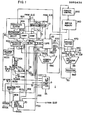
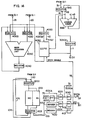
- Fig. 1 shows a configuration of an instruction unit (I-unit) 1 in the data processing system of the present invention
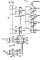
- Fig. 2 shows a configuration of an execution unit (E-unit) in the data processing system.
- numeral 960 denotes a buffer memory which is a high speed memory for temporarily storing data including instructions necessary for operation, of a content of a main memory (not shown)
- numeral 900 denotes an instruction buffer for temporarily storing instructions fetched from the buffer memory 960
- numeral 901 denotes an instruction partitioning circuit for fetching an instruction from one word of instruction in the instruction buffer 900
- numeral 902 denotes an instruction register to which the instruction fetched by the instruction partitioning circuit 901 is loaded.
- the instructions used in the data processing system of the present embddiment are same as those used in the IBM System /370 computer and they are classified into several formats.
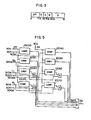
- an RX format instruction shown in Fig. 3 is used.
- the RX format instruction has 32 bits (bit 0 to bit 31), of which the bits 0-7 are an operation code to represent a type of instruction such as A or L, the bits 8-11 are a register field (R) representing a register number of a general purpose register in which an operand to be read out for the operation is stored or a register in which an operation result is to be stored, the bits 12-15 and the bits 16-19 are an index field (X) and a base field (B), respectively, which represent register numbers of I general purpose registers (IGPR) 60 and G general purpose registers (GGPR) 4050 to be described later, which are used to calculate an operand address, and the bits 20-31 are a displacement field (D) which represents a displacement used to calculate the general purpose register number based on the index field and the base field.
- the RX format instruction includes the A-instruction and the L-instruction.
- One word of the instruction buffer 900 comprises 72 bits and contains one or more instructions.
- the instruction partitioning circuit 901 partitions an instruction to be fetched from one word of instruction in the instruction buffer 901.
- Numeral 902A denotes a decision circuit which determines if the instructions stored in the instruction register 902 can be processed only by a main operation unit 4030 in the E-unit 2 shown in Fig. 2 and the operation results are to be stored in the IGPR 60, based on the operation codes of the instructions, and produces a "1" output if the decision is negative and "0" output if the decision is affirmative.
- Numeral 903 denotes an instruction queue register which sequentially stores first two bytes (bits 9-15) of instruction loaded in the instruction register 902 and the output of the decision circuit 902A to form an instruction execution queue, and numeral 904 denotes a work register in which the first two bytes of the instruction from the instruction queue register 903 are loaded.
- Numeral 9040 denotes a register in which an address of an operation result write register designated by the bits 8-11 of the instruction loaded in the register 904 is loaded
- numeral 9041 denotes a register in which an address of an operation result write register loaded in a register 3110 of Fig. 2 is loaded through a line 11
- numerals 904A and 904B denote comparators which compare the bits 8-11 (register field) of the instruction loaded in the register 904 with the content of the register 3110 in Fig. 2 and the content of the register 9041, respectively.
- Numeral 3 denotes an X/B conflict detector which detects the index/base register conflict in which the index register numbers or the base register members of the proceeding instruction and the succeeding instruction are equal, based on the contents of the registers 9040 and 9041 and the index field and the base field of the instruction loaded in the instruction register 902.
- Numeral 60 denotes the general purpose registers (GPR). In order to distinguish them from the general purpose registers 4050 in the E-unit 2 of Fig. 2, the GPR's of the I-unit 1 in Fig. 1 are referred to as IGPR's and the GPR's of the E-unit 2 are referred to as GGPR's.
- the GGPR's 4050 are of the same construction as the IGPR's 60 although it is not essential.
- the construction of the IGPR's 60 is shown in Fig. 4 and it has sixteen general purpose registers 8000-8015.
- Numeral 70 denotes a GPR write control which receives the outputs of the work register 904, the comparators 904A and 904B and the X/B conflict detector 3 and controls the storing of the operation results of the pre-operation unit 981 and the main operation unit 4030 into the IGPR's 60 and suppresses the stages to prevent an operand register conflict.
- the construction of the GPR write control 70 is shown in F ig. 6 to be explained later.
- Numeral 950 denotes an address control which converts a logical address determined by the address calculation into a physical address for reading out the buffer memory 960 and controls the fetching of the operand stored in the buffer memory 960
- numeral 970 denotes an operand buffer for storing the operand fetched from the operand buffer 960.
- Numeral 840 denotes a selector for selecting one of the index operands from the IGPR 60 and the operand buffer 970
- numeral 850 denotes a selector for selecting one of the base operands from the IGPR 60 and the operand buffer 970.
- the pre-operation unit 981 carries out the pre-operation for the operands supplied from the selectors 840 and 850 based on the operation code of the instruction loaded in the register 904 and it can process only the instructions such as A, L and TM (test mode) instructions which frequently appear and which require relatively small number of circuit components for the processing.
- the operation result is loaded in the register 982, thence it is stored in the IGPR 60 through a line 50.
- the main operation unit 4030 in the E-unit 2 of Fig. 2 can carry out the operation for all instructions including M (multiply) and D(divide) instructions which require a large scale of arithmetic and logic unit.
- Numeral 980 denotes an address adder which receives the bits 20-31 (displacement field D) of the instruction loaded in the instruction register 902, the base field data GR(B) from the IGPR 60 and the index field data GR(X) and adds them to produce an operand address.
- the output of the address adder 980 is supplied to the address control 950.
- the operation code, the register and index field and the base and index field are supplied from the instruction queue 903 of the I-unit 1 of Fig-1 to the E-unit 2 of Fig. 2 through lines 30, 31 and 31A, respectively, and the outputs of the selectors 840 and 850 are supplied to the pre-operation unit 981 and the E-unit 2 through lines 21 and 20, respectively.
- numeral 1000 denotes a register in which the operation code from the instruction queue 903 of the I-unit 1 is loaded
- numeral 1010 (#0 and #1) denotes a control storage for storing microprograms.
- a microinstruction fetched from the control storage 1010 in accordance with an address specified by the operation code of the instruction loaded in the register 1000 is loaded in a register 1001. If the microinstruction fetched loaded in the register 1001 is not the last microinstruction for the instruction initially loaded in the register 1000, a portion of the content of the register 1001 is added to the content of the register 1000 through a line 1012 to specify an address of a microinstruction to be next fetched from the control storage 1010 so that the next instruction is loaded to the register 1001 and the-microinstructions are sequentil- ly fetched. If the instruction loaded in the register 1001 is the last microinstruction, an end bit (EOP) is loaded in the register 1000 through a line 1012 and the next instruction is loaded in the register 1000 from the instruction queue 903.
- EOP end bit
- Numeral 4000 denotes a register in which the index operand from the selector 840 of the I-unit 1, or the index operand derived from the operation result of the operation unit 4050 or the data from the GGPR 4050 is loaded
- numeral 4010 denotes a register in which the base operand from the selector 850 of the I-unit 1, or the base operand derived from the operation result of the operation unit 4030 or the data from the GGPR 4050 is loaded.
- the operation result of the operation unit 4030 is stored in a register 4020.
- the operation unit 4030 carries out the operation on the index and base operands from the registers 4000 and 4010 in accordance with the microinstruction loaded in the register 1001, and the operation result is stored in a register 4040.
- Numeral 3110 denotes a register for storing the bits 0-15 of the instruction from the instruction queue 903 of the I-unit 1
- numeral 888 denotes an address adder which receives the bits 8-11 (register field) and 12-15 bits (index field) of the instruction loaded in the register 3110 and information +1 or +8 to calculate an address.
- the calculated address is stored in the register 3110.
- the 8-11 bits of the register 3110 are supplied to the GGPR 4050 as read address information for the GGPR 4050 and the bits 12-15 are supplied, after having been loaded in a register 3110A, to the GGPR 4050 as write address control information for the GGPR 4050.
- the content of the register 3110A is supplied to the register 9041 and the comparator 904A of the I-unit 1 through a line 11.
- the storing of the operation result of the main operation unit 4030 to the GGPR and the IGPR is controlled by the microinstruction.
- the main operation unit 4030 executes all instructions in the program including the instructions executed by the pre-operation unit 981.
- the same data as those stored in the IGPR 60 as the operation result of the pre-operation unit 981 are stored in the GGPR 4050 as the operation result of the main operation unit 4030.
- Numeral 4100 in the E-unit 2 denotes a decoder which decodes if the microinstruction loaded in the register 1001 specifies the storing of the operation result into the GGPR 4050.
- the decoded result is set in a flip-flop 4101 and supplied to the GGPR 4050 as a write enable signal.
- Numeral 4200 denotes a decoder which decodes if the microinstruction loaded in the register 1001 specifies the storing of the operation result into the IGPR 60.
- the decoded result is set in a flip-flop 4102 and supplied to the IGPR 60 through a line 100 as a write control signal.
- Numeral 5000 denotes a flip-flop in which a decision result by the decision circuit 902A for the instruction from the instruction queue 903 is set.
- the decision result set in the flip-flop 5000 is sent to the GPR write control 70 and the X/B conflict detection 3 of the I-unit 1 through a line 5000A and it is also set in a flip-flop 5010, thence it is sent to the GPR write control 70 and the X/B conflict detector 3 through a line 5010A.
- both the operation result of the pre-operation unit 981 and the operation result of the main operation unit 4030 but not of the pre-operation unit are stored in the IGPR 60. Accordingly, in comparison with a case where the operation result of the pre-operation is stored in a separate buffer, the index and base operands to be used for the address calculation are supplied to the address adder from only the IGPR 60 and no selector for selecting the information from the GPR and the buffer is required.
- the write register number for the instruction set in the register 904 and the write register number for the preceding instruction in the program loaded in the register 3110A from the instruction queue 903 through the register 3110 are compared by the comparator 904A, and in the next machine cycle, the write register number for the instruction loaded in the register 904 and the write register number for the preceding instruction loaded in the register 904 from the register 3110A are compared by the comparator 904B, and compare results for both comparisons are sent to the GPR write control 70.
- Signals indicating whether the preceding instructions loaded in the register 3110A and then in the register 9041 in two consecutive machine cycles cannot be processed by the pre-operation unit 981 and the operation results for those instructions by the main operation unit are to be stored in the IGPR 60 are sent to the GPR write control 70 from the flip-flops 5000 and 5010.
- the GPR write control 70 responds to those signals and produces a stage suppress signal on a line 803A if the write register number for the instruction loaded in the register 904 and the write register number for the preceding instruction loaded in the register 3110A are equal and the operation result for the preceding instruction should be stored in the IGPR 60, or if the write register number for the instruction loaded in the register 904 and the write register address for the preceding instruction loaded in the register 9041 are equal and the operation result for the preceding instruction should be stored in the IGPR 60.
- stage suppress signal By the stage suppress signal, the execution of the stages D , A, L and E for the succeeding instructions in the program loaded in the register 904 is suppressed, and if it is determined from the operation code supplied from the register 904 that the succeeding instruction can be pre-operated and the operation result should be stored in the IGPR 60, the storing of the operation result of the pre-operation unit 981 into the IGPR 60 is inhibited. In this manner, when the operand register conflict occurs, the storing of the operation result for the succeeding instruction into the IGPR 60 is permitted after the storing of the operation result for the preceding instruction into the IGPR 60.
- a plurality of instructions are previously stored in the buffer 900 from the buffer memory 960. Each instruction is loaded to the instruction register 902 by the instruction partitioning circuit 901 prior to the start of the D-stage. If the instruction is of the RX format which generates one operand address from the index address, base address and the displacement, the index register address (X) and the base register address (B) are sent to the IGPR 60 through the lines 53 and 54, respectively, in the D-stage. The data GR(X) and GR(B) read from the I G P R 60 by the index register address X and the base register address B, respectively, and the displacement of the instruction are sent to the address adder 980 where an operand address is calculated. The first two bytes of the instruction (.
- the decision circuit 902A determines, based on the operation code in the instruction register 902, if the instruction can be processed only by the main operation unit 4030 and the operation result should be stored in the IGPR 60, and the decision result is paired with the first two bytes of the instruction in the instruction register 902 and the pair is stored in the instruction queue 903. If the decision is negative, the decision result is "1", as described before.
- the operand address calculated by the address adder 980 in the D-stage is converted to a physical address for the buffer memory by the address control 950 in the A-stage, and the operand is fetched from the buffer memory 960 and it is stored in the operand buffer 970.
- the output of the operand buffer 970 is selected by the selector 840 and supplied to the pre-operation unit 981.
- the first two bytes of the instruction from the instruction queue 903 is loaded to the register 904 and the register field of the instruction which represents the address (Rl) of the IGPR 60 which stores the other operand to be used by the instruction is sent to the IGPR 60 through the line 55.
- the operand GR(Rl) fetched from the IGPR 60 based on the address Rl is sent to the selector 850 through the line 820, selected by the selector 850 and supplied to the pre-operation unit 981.
- the first two bytes of the instruction from the instruction queue 903 are of a format (RR format) which uses the data in two general purpose registers of the IGPR 60 as the operands
- the other IGPR address (R2) for the other operand than the address (Rl) is sent to the IGPR 60 through the line 56
- the operand GR(R2) read out based on the address R2 is sent to the selector 850 through the line 830 and selected by the selector 850 and supplied to the pre-operation unit 981.
- a microcode for specifying a start address of a microprogram for the microprogram processing in the subsequent E-stage is sent from the instruction queue 903 to the E-unit 2 through the output line 30.
- the first byte of the instruction which contains the read and write addresses for the GGPR 4050 is sent to the E-unit 2 through the line 31.
- the decision result of the decision circuit 902A from the instruction queue, which is used as an I G PR write request signal in the P-stage is sent to the E-unit 2 through the line 31A.
- the storing of those signals sent to the E-unit 2 into the registers in the E-unit 2 is carried out in the next stage.
- the instruction loaded in the register 904 can be operated by the pre-operation unit 981
- the operands GR(Rl) and GR(R2) read from the IG PR 60 in the A-stage are operated by the pre-operation unit 981 and the operation result is loaded in the register 982.
- the two operands are also sent to the registers 4000 and 4010 in the E-unit 2 through the lines 20 and 21.
- the write register address in the bits 8-11 of the instruction loaded in the register 904 is loaded in the register 9040 through the line 800.
- the start address of the microprogram sent from the instruction queue 903 through the line 30 in the A-stage is loaded to the address register 1000 and the microinstruction is fetched from the control storage 1010 and supplied to the register 1001.
- the first byte of the instruction sent from the instruction queue 903 through the line 31 in the A-stage is loaded to the register 3100.
- the decision result of the decision circuit 902A sent from the instruction queue 903 through the line 31A in the A-stage is set in the flip-flop 5000.
- the operation result loaded in the register 982 by the write register address on the line 52 of the register 9040 is stored in the IGPR 60 through the line 50.
- the operands sent from the selectors 840 and 850 through the lines 20 and 21 in the L-stage are loaded to the work registers 4000 and 4010 and they are operated by the operation unit 4030 under the control of the microinstruction, and the operation result is stored in the register 4040.
- the write register field (for the RX format instruction, the bits 8-11 of the register 3110 are the write address) which represents the write address in the first byte of the instruction from the instruction queue 903 represetning the content of the register 3110 loaded in the L-stage is sent to the comparator 904A of the I-unit 1 through the line 11 and loaded in the register 9041 of the I-unit 1 in the E-stage.
- the decision result of the decision circuit 902A set in the flip-flop 5000 is set in the flip-flop 5010 in the E-stage and sent to the GPR write control 70 in the I-unit 1 through the line 5010A.
- the microinstruction fetched in the L-stage is loaded in the register 1001.
- the microprogram instructions are sequentially fetched into the register 1001, and after the microprogram for the instruction loaded in the register 1000 has been completed, the next instruction is loaded in the regiser 1000 from the instruction queue 903. If the instruction which requires the GGPR write is loaded in the register 1000 and if the microinstruction which requires the storing of the operation result into the GGPR is loaded in the register 1001, the content of the instruction is decoded by the decoder 4100 through the output line 1013 and the decoded result is set in the flip-flop 4101 and sent out through the line 58 as a write enable signal to the GGPR 4050.
- the identification information is decoded by the decoder 4200 through the output line 1002 and the decoded result is set in the flip-flop 4102 and sent to the IGPR 60 of the I-unit 1 through the line 100 as the IGPR write signal.
- the operation result in the E-unit 2 is loaded in the register 4020 from the register 4040 under the control of the microinstruction and it is sent to the GGPR 4050 through the line 4020A. If the instruction cannot be operated by the pre-operation unit 981, the operation result is sent to the GGPR 4050 and the output of the register 4020 is sent to the IGPR 60 of the I-unit 1 through line 10 as the data to be stored in the IGPR 60. The data from the register 4020 is stored in the IGPR 60 in response to the I GPR write signal sent from the flip-flop 4102.
- stage suppress signal 803A is "1"
- the D, A, L and E stages are suppressed. A detail of the operation will be explained with reference to Fig. 10.
- Fig. 4 shows a detail of the IGPR 60 of Fig. 2 which is a characteristic feature of the present invention.
- the write and read operations of the general purpose registers of the IGPR 60 are now explained with reference to Fig. 4.
- the IGPR 60 ' includes sixteen general purpose registers 8000 - 8015 (GPRO - GPR15) outputs.of which are connected to multiplexers (MPX) 53A, 53B, 53C and 53D.
- the MPX 53A selects one of the general purpose registers by the index resiger address X supplied from the instruction register 902 through the line 53 and sends the content of the selected register to the address adder 981 through the line 800 as the data R(X).
- the MPX 53B selects one of the general purpose registers by the base register address B designated by the instruction register 902 through the line 54 and sends the content of the selected register to the address adder 981 through the line 810 as the data R(B)
- the NPX 53C selects one of the general purpose registers by the register address Rl supplied from the instruction queue 903 through the line 55 and sends the content of the selected register to the selector 850 through the line 820 as the data R(l)
- the ⁇ MPX 53D selects one of the general purpose registers by the register address R2 supplied from the instruction queue 903 through the line 56 and sends the content of the selected register to the selector 840 through the line 830 as the data R2.
- the contents of the four general purpose registers of the IGPR 60 can be independently read out.
- the operation result for the instruction which can be operated by the pre-operation unit 981 is stored in the IGPR 60 in the E-stage and the operation result for the instruction which cannot be operated by the pre-operation unit 981 is stored in the IGPR 60 in the P-stage.
- the write data from the register 4020 of the E-unit 2 is sent to the GPR's 8000 - 8015 through the line 10.
- the write data from the pre-operation unit 981 is sent to the GPR's 8000 - 8015 through the line 50.
- the GPR address supplied from the register 3100 of the E-unit 2 through the register 9041 is sent to the decoder 61 shown in Fig.
- the decoded data is sent to the lines 630 - 645 through an AND gate which receives the IGPR write signal from the flip-flop 4102 of the E-unit 2.
- the GPR address which represents the write address for the operation result of the pre-operation unit 981 is sent to the decoder 62 of Fig. 4 through the line 52 and decoded thereby, and the decoded data is sent to the lines 650 - 665 through an AND gate which receives the IGPR write enable signal from the GPR write control 3 through the line 700.
- the write signal in the P-stage on the line 630 and the write signal in the E-stage on the line 650 are sent to the line 530 through an OR gate to produce a set signal to the GPR 8000.
- the signals on the lines 631 - 645 and the signals on the lines 651 - 665, respectively, are also sent to the lines 531 - 545, respectively, through OR gates to produce set signals to the GPR's 8001 - 8015.
- Whether the data on the line 10 or the line 50 is to be supplied to the GPR 8000 is designated by the signal on the line 630. If the signal on the line 630 is "1", the signal on the line 10 is selected, and if it is "0" the signal on the line;50 is selected.
- the input data are selected by the signals on the lines 631 - 645. In this manner, the data can be simultaneously written in the general purpose registers of the IGPR 60 in the E-stage for the current instruction and the P-stage for the preceding instruction.
- Fig. 5 shows a detail of the X/B conflict detector 3 in the I-unit 1
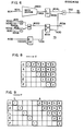
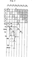
- Fig. 7 shows a flow chart for the pipeline therefor.
- D.A.L.E and P represent the respective stages and an abscissa represent a time in machine cycle unit.
- Each machine cycle is divided by four clocks, each designated by T 0 , T 1 , T 2 and T 3 .
- a clock T i for the machine cycle is designated in combination with the stage such as clock (D, T i ).
- Numbers 1 - 5 in Fig. 7 represent the instruction numbers to be processed.
- 1 represents a L(load)-instruction
- 2 represents an A (add)-instruction.
- the write register number Rl for 1 and the index register number R2 for 22 are equal and hence the index register conflict occurs.
- Fig. 8 shows a pipeline flow where the index register conflict does not occur
- Fig. 9 shows a pipeline flow for the prior art system where the index register conflict occurs and the pre-operation is not carried out.
- the operation result can be stored in the IGPR 60 in the E-stage. Accordingly, the D-stage for the A-instruction 2 can be processed in overlap with the E-stage for the L-instruction 1 and the operand address necessary for the A-instruction can be obtained. As a result, in comparison with Fig. 9, the D-stage for the A-instruction 2 can be initiated two cycles earlier.
- the L-instruction 1 is loaded in the instruction register 902 at a clock.T O (D, T 0 ) in cycle C 1 . Since the L-instruction 1 can be operated by the pre-operation unit 981, the output "0" from the decision circuit 902A is loaded in the instruction queue 903 at a clock TO (A, T 0 ) in cycle C 2 . The first two bytes of the instruction register 902 are also loaded in the instruction queue 9 0 3 at the clock T 0 (A, T 0 ). At a clock to of the cycle C 2 , the A-instruction 2 is loaded in the instruction register 902.
- the index field X and the base field B of the A-instruction 2 are sent from the instruction register 902 to the X/B conflict detector 3 through the lines 53 and 54.
- the write register number R l of the L -instruction 1 is sent from the instruction queue 903 to the X/B conflict detector 3 through the line 903A.
- the X/B conflict detector 3 which is shown in detail in Fig. 5, the index field of the A-instruction 2 from the instruction register 902 and the register number Rl of the L-instruction 1 from the instruction queue 903 are compared by a comparator 10000. Since the addresses are equal in the present example, the output of the comparator 10000 passes through an OR gate and renders the D-stage suppress signal 3A to "1". By this signal, the processing in the D-stage for the A-instruction 2 at the cycle C 2 is suppressed and the update of the instruction register 902 is suppressed.
- the first two bytes of the L-instruction 1 including the write address Rl are loaded in the register 904.
- the four bits of the register 904 including the write address Rl are loaded in the register 9040 at a clock TO (L, T 0 ) in cycle C 3 .
- the data X and B of the A-instruction 2 are sent to the lines 53 and 54 at the clock T 0 of the cycle C 3 .
- the write address Rl of the L-instruction 1 is sent from the register 9040 to the line 52.
- a comparator 10010 of the X/B conflict detector 3 compares the index field of the A-instruction 2 from the instruction register 902 on the line 53 and the address Rl of the L-instruction 1 from the register 9040 on the line 52.
- an output of the comparator 10010 passes through an OR gate to render the D-stage suppress signal 3A to "1". This signal is sent to a stage control circuit, not shown to suppress the D-stage so that the D-stage for the A-instruction 2 in the cycle C 3 is suppressed.
- the output of the decision circuit 902A representing the IGPR write request in the P-stage is sent to the E-unit 2 through the line 31A and it is set in the flip-flop 5000 at a clock T 2 (L, T 2 ) in the cycle C 3 and sent to the I-unit 1 through the line 5000A.
- the write address Rl of the L-instruction 1 is sent to the E-unit 2 through the line 31, and at a clock T 0 (L, T 0 ) of the cycle C 31 it is loaded in the register 3110 and the bits 8-11 of the register 3110, that is, the address Rl of the L-instruction 1 , are loaded in the register 3110A, and at a clock T 2 (L, T 2 ) of the cycle C 3 they are sent to the I-unit 1 through the line 11.
- the write address Rl of the L-instruction is sent to the line 11 and the comparator 10020 of the X/B conflict detector 3 compares the register address Rl of the L-instruction from the register 3110A on the line 11 and the index field of the A-instruction from the instruction register 902 on the line 53.
- the addresses are equal and the IGPR write request signal supplied from the flip-flop 5000 through the line 5000A in the P-stage is "0". Therefore, the compare result is suppressed by the AND gate and the D-stage suppress signal 3A is "0". Accordingly, the D-stage for the A-instruction 2 is processed in the cycle C 4 .
- the L-instruction can be operated by the pre-operation unit 981 but if the instruction 1 cannot be operated by the pre-operation unit 981 the IGPR write request signal supplied from the flip-flop 5000 in the P-stage is "1" and the D-stage suppress signal 3A is "1" in the cycle C 4 so that the operation in the D-stage is suppressed.
- the IGPR write request signal supplied from the flip-flop 5010 through the line 5010A in the P-stage is "1" and the D-stage suppress signal 3A is "1” so that the operation in the D -stage is suppressed.
- the D-stage for the instruction 2 is first processed. In this case, the pipeline flow is same as that shown in Fig. 9.
- the index register has thus been described in connection with the comparators 10000-10030 as to the base register 54, the addresses are compared by the comparators 10040-10070 and the D-stage suppress signal 3A is rendered to "1" as required in the same manner as for the index register.
- Fig. 6 shows a detail of the GPR write control 70 which is a characteristic feature of the present invention. The operation thereof is explained with reference to Figs. 10 - 12.
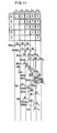
- Fig. 10 shows a pipeline flow chart where the instructions (for example, L-instructions) which can be operated by the pre-operation unit 981 and the operation results of which should be stored in the general purpose registers appear successively.
- instructions for example, L-instructions
- the instructions 1 - 5 are RX instructions for writing in the general purpose registers. Accordingly, the GPR write address is designated by Rl.
- the instruction 1 is loaded in the instruction register 902 at the clock TO (D, T 0 ) of the cycle C 1 . Since the instruction 1 can be operated by the pre-operation unit 981, the decision circuit 902A produces the output "0" and this output and the first two bytes of the instruction are loaded in the instruction queue 903 at the clock TO (A, T 0 ) of the cycle C 2 .
- the data including the write address Rl, loaded at the clock T 0 (A, T 0 ) of the cycle C 2 is loaded to the register 904 through the line 903A at the clock T 2 (A, T 2 ) of the cycle C 2 .
- the operation code of the register 904 is supplied to the GPR write control 70 shown in detail in Fig.6 through the line 804.
- the GPR write decision circuit 9990 in Fig. 6 determines that the instruction 1 can be operated by the pre-operation unit 981 and the GPR writing is requested and produces a "1" output on the line 9901. This "1" output is set in the flip-flop 9902 at the clock T 2 of the cycle C 3 .
- the output of the decision circuit 902A on the output line 3A which was set to "0" at the clock T 2 (A, T 2 ) of the cycle C 2 is set in the flip-flop 5000 at the clock T 2 (L, T 2 ) of the cycle C 3 as shown in Fig. 10 and the output is produced on the line 5000A. It is also set in the flip-flop 5010 at the clock T 2 of the cycle C 4 to produce a "0" output on the line 5010A.
- the microinstruction address supplied from the instruction queue 903 through the line 30 at the clock TO (A, T 2 ) of the cycle C 2 is loaded in the register 1000 of the E-unit 2 at the clock T 0 (L, T 0 ) of the cycle C 3 .
- the microinstruction is fetched from the control storage 1010 and it is loaded in the register 1001 at the clock T 2 (L, T 2 ) of the cycle C 3' Since the instruction 1 requests the GPR writing, the GPR write instruction is stored in the register 1001 and it is decoded by the decoder 4100 and the decoded output is set in the flip-flop 4101 at the clock T 2 (E, T 2 ) of the cycle C 4 so that a "1" output is produced on the output line 58. This is the write instruction to the GGPR 4050. Since the writing into the IGPR 60 is not required in the P-stage for the instruction 1, the IGPR write instruction is not supplied from the register 1001 to the decoder 4200.
- the instruction 2 is loaded in the instruction register 902 at the clock TO (D, T 0 ) of the cycle C 2 .
- the two bytes of the instruction 2 are read out from the instruction queue 903 to the line 903A and it is loaded in the register 904 at the clock T 2 (A, T 2 ) of the cycle C 3 and the write register address is supplied to the line 800 from the register 904 and the operation code of the register 904 is supplied to the GPR write control 70 shown in Fig. 6 through the output line 804.
- the signal on the line 5000A from the flip-flop 5000 is "0" and the instruction preceding to the instruction 1 can be pre-operated
- the signal on the line 5010A from the flip-flop 5010 is also "0” and "0" output is produced on the line 9000 through the AND gate and the OR gate so that the flip-flop 9001 is not set at the clock T 2 (L, T 2 ) of the cycle C 4 and the inverted output 9010 of the flip-flop 9001 is "l”.
- the signal on the line 904L from the flip-flop 9902 and the signal on the line 9010 from the inverted output of the flip-flop 9001 are ANDed to produce the IGPR write enable signal 700.
- the stage suppress signal on the line 803A is "0".
- the instruction 3 like the instruction 2 , "1" is set in the flip-flop 9902 at the clock T 2 (L, T 2 ) of the cycle C 5 and the "1" output is produced on the line 904L.
- the signal on the line 5000A from the flip-flop 5000 is "0" and the signal on the line 5010A from the flip-flop 5010 is "0".
- the stage suppress signal on the line 804A is "0" and the pipeline flows without disturbance.
- the signal on the line 803A is sent to the stage control circuit, not shown, to suppress the D, A, L and E-stages for the succeeding instructions.
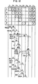
- Fig. 11 shows a pipeline flow chart where the instruction 1 cannot be operated by the pre-operation unit 981 and the instructions 2 ,.3 , 4 and 5 can be pre-operated and the GPR write addresses of the instructions 2 and 3 are different from the G PR write address of the instruction 1.
- the operation of the instruction 1 is identical to that of the instruction 1 of Fig. 10 with the following exception. Since the instruction 1 cannot be operated by the pre-operation unit 981, it is determined by the decision circuit 902A, which produces "1" output. This output is loaded in the instruction queue 903 at the clock TO of the cycle C 2 . This signal is supplied to the flip-flop 5000 of the E-unit 2 through the output line 31A of the instruction queue 903 and operated in the same manner as Fig. 10.
- the instruction 2 can be operated by the pre-operation unit 981 and the operation is identical to that of Fig. 10 with the following exception.
- the write register address of the instruction loaded in the register 967 at the clock T 2 of the cycle C 3 is compared with the write register address of the instruction 1 loaded in the register 3110A of the E-unit 2 at the same time, by the comparator 904A. Since those addresses are not equal as described above, the comparator 904A produces "0" signal on the line 803.
- the AND gate which AND's the signal on the line 904L from the flip-flop 9902 and the signal on the line 9010 from the inverted output of the flip-flop 9001 is opened so that the IGPR write signal is produced on the line 700. Accordingly, the stage suppress signal on the line 803A is "0".
- the write register address on the line 800 loaded in the register 904 at the clock T 2 of the cycle C 4 is compared with the register write address of the instruction 1 on the line 801 loaded in the register 9041 at the same time, by the comparator 904B. Since those addresses are not equal as described above, the comparator 904b produces "0" signal on the line 802. Since the signal on the line 5010A from the flip-flop 5010 is "1" at this time but the signal on the line 802 is "0", one of the AND gates in Fig. 6 is not opened. Since the signal on the line 5000A from the flip-flop 5000 is "0" (because the instruction 2 can be operated by the pre-operation unit 981), the other AND gate is also not opened.
- the flip-flop 9001 is not set at the clock T 2 .of the cycle C 5 and "1" signal is produced at the inverted output of the flip-flop 9001. Thereafter, the AND gate which AND's the signal on the line 904L and the signal on the line 9010 is opened and the IGPR write enable signal is produced on the line 700. At the some time, the stage suppress signal on the line 803A becomes "0". In this manner, the pipeline flows as shown in Fig. 8.
- Fig. 12 shows a pipeline flow chart where the instruction 1 cannot be operated by the pre-operation unit 981 and the instructions 2 . 3 , 4 and 5 can be pre-operated and the GPR write addresses of the instructions 1 and 2 are equal.
- the operation of the instruction 1 is same as that of the instruction 1 of Fig. 11 and hence it is not explained here.
- the operation of the instruction 2 is same as that of Fig. 10 with the following exception.
- the write register address of the instruction loaded in the register 904 at the clock T 4 of the cycle C 3 is compared with the write register address of the instruction 1 loaded in the register 3110A of the E-unit 2 at the same time, by the comparator 904A. Unlike the case of Fig.
- the write addresses are compared and if they are not equal, the writing is permitted and if they are equal the writing is delayed by delaying the GPR write signal from the pre-operation unit 981.
- the addresses are equal, the operation by the pre-operation unit 981 is given up even if the instruction can be operated by the pre-operation unit 981 and it is operated by the main operation unit 4030.
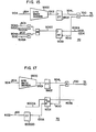
- the instruction unit of Fig. 1 is replaced'by that of Fig. 13
- the execution unit of Fig. 2 is replaced by that of Fig. 14
- the GPR write control of Fig. 6 is replaced by that of Fig. 15.
- the IGPR write signal 100 is isolated from the input and the line 803A for carrying the stage suppress signal is blocked. Instead, the IGPR write request signal from the main operation unit 4030 is supplied to the line 1002A.
- the instruction 1 cannot be operated by the pre-operation unit 981 and the instructions 2 , 3 , 4 and 5 can be pre-operated and the GPR write addresses of the instructions 1 and 2 are equal.
- the operation of the instruction 1 is identical to that of the instruction 1 of Fig. 12.
- the operation of the instruction 2 is explained below.
- the write register address of the instruction loaded in the register 904 at the clock T 2 of the cycle C 3 is compared with the write register address of the instruction 1 loaded in the register 3110A of the E-unit 2 at the same time, by the comparator 904, and if those addresses are equal, the flip-flop 9001 is set at the clock T 2 of the cycle C 4 instead of producing the stage suppress signal on the line 803A in Fig. 6, to supply the IGPR write request signal from the main operation unit to the line 1002A.
- the IGPR write is not allowed at the clock T 2 of the cycle C 4 and "0" signal is produced on the line 700.
- Fig. 14 unlike in Fig. 2, in order to operate the instruction O2 by the main-operation unit 4030, the output from the flip-flop 5000 and the signal on the line 1002A are ORed by the OR gate 1003 at the clock T 2 of the cycle C 4 and the IGPR write signal from the main operation unit is supplied to the line 500A.
- the output of the OR gate 1003 is set in the flip-flop 5010.
- the output of the decoder 4200 and the signal on the line 1002A are ORed by the OR gate 1004 to set the flip-flop 4102.
- the instruction 2 is regarded as the instruction which cannot be operated by the pre-operation unit 981.
- the IGPR write signal "1" of the instruction 1 is produced on the line 100 at the clock T 2 of the cycle C 4 and the IGPR write signal "1" of the instruction 1 is produced on the line 100 at the clock T 2 of the cycle C 5 . In this manner, the writing is delayed without the stage suppress signal.
- the write addresses are compared and if they are not equal, the writing is permitted, and if they are equal, the writing is delayed. In an alternative method, no comparison is made and the writing is unconditionally delayed. An embodiment thereof is shown in Figs. 16, 17 and 18. Only the differences from Figs. 1 to 12 are explained.
- Fig. 16 shows a detail of the I-unit 1 which corresponds to that of Fig. 1.
- the comparators 904A and 904B of Fig. 1 are not necessary and they are omitted, and the inputs to the GPR write control 70 are only those on the lines 5000A, 804 and 100 from the flip-flop 5000, the register 904 and the flip-flop 4102 of the E-unit 2, respectively.
- the execution unit and the GPR's of the third embodiment are identical to those of the first embodiment shown in Figs. 3 and 4, respectively.
- a further detail of the GPR write control which is a characteristic feature of the present embodiment is shown in Fig. 17. It corresponds to Fig. 6 in the first embodiment.
- the operation is explained with reference to Fig. 18.
- the instruction 1 cannot be operated by the pre-operation unit 981 and the instructions 2 , 3 , 4 and 5O can be pre-operated. It includes the both cases of Figs. 11 and 12 of the first embodiment.
- the GPR write addresses of the instructions 2 and are not equal or equal to the GPR write address of the instruction 1 the operation is the same.
- Fig. 18 The operation of Fig. 18 is similar to that of F ig. 12 described above. Only the difference from the operation of Fig. 12 is explained below.
- the operation of the instruction 1 is same as that of the instruction 1 in F ig. 12.
- the operation of the instruction 0 is similar to that in Fig. 12 with the following exception.
- the write register address of the instruction loaded in the register 914 at the clock T 2 of the cycle C 3 is not compared with the write register address of the instruction loaded in the register 3110A of the E-unit 2 at the same time.
- the flip-flop 9001 is set only by the signal on the line 5000A from the flip-flop 5000 without comparing the addresses. As a result, the circuit of the GPR write control 70 is simplified.
- a read register address field is included in addition to a write register address field.
Abstract
Description
- The present invention relates to a pipelined data processing system, and more particularly to a pipelined data processing system in which an instruction is executed in a plurality of stages each having an independent hardware and the stages are operated in an overlapped mode.
- In a prior art pipelined data processing system, an instruction is executed in five to seven stages with each stage being operated in one machine cycle (basic cycle of the data processing system) and the stages being operated in an overlapped mode so that each instruction is apparently executed in one cycle.
- By way of example, let us assume that an instruction is processed in five stages, that is, a D-stage in which the instruction is decoded and an operand address is determined by adding a content of a general purpose register designated by an index field of the instruction, a content of a general purpose register designated by a base field of the instruction and a content of a displacement field of the instruction; an A-stage in which the logical operation address determined in the D-stage is converted to a physical address actually used to access a memory, an L-stage in which an operand is fetched from a buffer memory which is a high speed memory containing a portion of data of a main memory, or from a general purpose register based on the physical address converted in the A-stage; an E-stage in which an operation is carried out using the operand fetched in the L-stage; and a P-stage in which an operation result is stored in the memory or the general purpose register. For example; the D-stage for an
instruction ① is processed in one machine cycle of the data processing system and the A-stage for theinstruction ① is processed in the next machine cycle and the D- stage for the succeedinginstruction ② is simultaneously processed, and similarly the succeedinginstructions - Approaches to reduce such a delay have been proposed by Japanese Patent Publication 9088/82 and Japanese Patent Application 194002/81 (corresponding to U.S. Serial 446002) both filed by Hitachi Ltd., the same assignee as the present assignee), in which in addition to a main operation unit which can carry out operations required by any instruction, a pre-operation unit capable of carrying out only simple operations (many of the instructions which cause the address conflict such as the L-instruction and the A-instruction can be processed by an operation unit having a relatively small number of component circuits) is arranged in a vicinity of a hardware unit for the D-stage so that the operation result of the preceding instruction is produced earlier by the pre-operation unit and it is utilized to . process the succeeding instruction. In this manner, the delay of the data processing due to the address conflict can be reduced. However, in the system disclosed in the Japanese Patent Publication 9088/82, a buffer memory for storing the output of the pre-operation unit is not provided and hence the pre-operation can be carried out only for the immediately preceding instruction to the current instruction. In the system disclosed in the Japanese Patent Application 194002/81, a buffer for storing the output of the pre-operation unit is provided but the buffer is separately arranged from a general purpose register. Accordingly, the number of circuit components required is large. In the system of the Japanese Patent Publication 9088/82, it is necessary to select an index for an address calculator for calculating an address to process the instruction from the general purpose register or the pre-operation unit and hence a selector is needed. In the system of the Japanese Patent Application 194002/81, a selector for selectively reading an index from the general purpose register or the buffer to the address calculator is needed and hence additional circuit components for the selector are required.
- It is an object of the present invention to provide a pipelined data processing system having a high processing speed which resolves the problems encountered in the prior art.
- In the data processing system of the present invention, in order to prevent the degradation of the system performance due to the address conflict, a pre-operation unit is provided in addition to a main operation unit and both outputs of the main operation unit and the pre-operation unit are stored in general purpose registers.
- By storing the output of the pre-operation unit in a plurality of general purpose registers, the pre-operation can be carried out for the preceding instruction other than the immediately preceding instruction and the operation result can be stored for use by the succeeding instruction. By storing the outputs of the both operation units in the general purpose registers, the number of circuit components required for the buffer, the selector and the control therefor is significantly reduced in comparison with the case where the output of the pre-operation unit is stored in a buffer other than the general purpose register.
- In storing the outputs of both the main operation unit and the pre-operation unit in the general purpose register, it may happen that an operation result different from that which would be obtained when a plurality of instructions are processed in a programmed sequence is stored in the general purpose registers. By way of example, let us assume that instructions I1, I 2' I 3' I4 and I5 are to be processed and the those instructions are to.be processed in the order of I1, I2' I5 by the program, and the instructions I1. I3' I4 and IS can be processed by the pre-operation unit while the instruction I2 cannot be processed by the pre-operation unit but it is processed by the main operation unit. In the execution of the instructions I1 through I5, the operation results for the instructions I1. I3' I4 and I5 by the pre-operation unit are stored in the general purpose register in the order of the processing of those instructions but the operation result for the instruction I2 is obtained later because the instruction I2 is processed by the main operation unit. Accordingly, the operation result for the instruction I2 is stored in the general purpose register simultaneously with or later than the storing of the operation result of the instruction I3 into the general purpose register. In other words, the operation result for the instruction I3 is stored in the general purpose register simultaneously with or earlier than the storing of the operation result for the
instruction 12 into the general purpose register. Therefore, if the program is constructed such that the operation results for the instructions I2 and I3 are to be stored in the general purpose register of the same address (this being called an operand register conflict), the content of the register to which the operation result for the instruction I3 has been stored is subsequently replaced by the operation result for the instruc- tion 12. As a result, a data other than the operation result for the instruction I3, which are expected to be processed in the order of the instructions I1. I2' ... I5 by the program, is left in the register. - In order to resolve the above problem, in accordance with one embodiment of the present invention, there is provided means for storing the operation result for the succeeding instruction into the general purpose register after the operation result for the preceding instruction in the program has been stored in the general purpose register. The following two approaches for such means are disclosed herein.
- In one approach, addresses of the general purpose registers to which the operation results for two instructions in a sequence of instructions in the program, for example, the instructions I2 and I3, are to be stored are compared, and if they are not equal, it is permitted to store the operation result for the instruction I3 into the register prior to the storing of the operation result for the
instruction 12 into the register, and if the addresses are equal, the storing of the operation results for the instruction I3 and the succeeding instructions is inhibited into the register until the storing of the operation result for the instruction I2 into the register is completed. In this case, the address of the register to which the operation result for the instruction I2 is to be stored and the addresses of the registers to which the instructions other than the instruction I3, for example, the instruction I4, are to be stored are compared and similar processing is carried out. - In another approach, the storing of the operation results for the instruction I3 and the succeeding instructions into the registers is unconditionally inhibited until the storing of the operation result for the instruction I2 into the register is completed without regard to whether the addresses of the registers to which the operation results for the
instructions 12 and I3 are to be stored are equal or not. - The above and other features and advantages of the present invention will be apparent from the following description taken in conjunction with the accompanying drawings, in which:
- Fig. 1 shows a detail of an instruction unit in a first embodiment of a data processing system,
- Fig. 2 shows a detail of an execution unit in the first embodiment,
- Fig. 3 shows an instruction format used in the data processing system,
- Fig. 4 shows a detail of a general purpose register shown in Fig. 2,
- Fig. 5 shows a detail of an X/B conflict detector shown in Fig. 2,
- Fig. 6 shows a detail of a general purpose register write control shown in Fig. 2,
- Fig. 7 shows a chart for explaining instruction processing in the first embodiment of the present invention,
- Fig. 8 shows a chart for explaining instruction processing where no index register conflict occurs in a pipelined data processing system,
- Fig. 9 shows a chart for explaining instruction processing without pre-operation where an index register conflict occurs in the pipelined data processing system,
- Fig. 10 shows a chart for explaining instruction processing where instructions which can be processed by a pre-operation unit are in series and operation results thereof are to be stored in general purpose registers,
- Fig. 11 shows a chart for explaining one instruction processing where an instruction which cannot be pre-processed is followed by instructions which can be pre-processed,
- Fig. 12 shows a chart for explaining another instruction processing where an instruction which can be pre-processed is followed by instructions which can be pre-processed,
- Fig. 13 shows a detail of an instruction unit in other embodiment of the present invention,
- Fig. 14 shows a detail of an execution unit in the other embodiment of the present invention,
- Fig. 15 shows a detail of a general purpose register write control shown in Fig. 13,
- Fig. 16 shows a detail of an instruction unit in a further embodiment of the present invention,
- Fig. 17 shows a detail of a general purpose register write control shown in Fig. 16, and
- Fig. 18 shows a chart for explaining instruction execution in Fig. 13.
- One embodiment of the present invention is now explained. The present embodiment can execute instructions used in the IBM System /370 computer. The operation of this system is described in "IBM System /370 Principle of Operations" published by IBM. In the present specification, therefore, the explanation of the operation of the above system is omitted unless specifically needed and the terms used therein are used without explanation unless specifically needed. In the data processing system of the present invention, one instruction is executed in a pluality of stages and the instructions are executed in a pipeline fashion such that different stages for different instructions are executed in parallel. In the present embodiment, the stages D, A, L, E and P are executed as is done in the prior art.
- Fig. 1 shows a configuration of an instruction unit (I-unit) 1 in the data processing system of the present invention, and Fig. 2 shows a configuration of an execution unit (E-unit) in the data processing system. In Fig. 1,
numeral 960 denotes a buffer memory which is a high speed memory for temporarily storing data including instructions necessary for operation, of a content of a main memory (not shown),numeral 900 denotes an instruction buffer for temporarily storing instructions fetched from thebuffer memory 960,numeral 901 denotes an instruction partitioning circuit for fetching an instruction from one word of instruction in theinstruction buffer 900, andnumeral 902 denotes an instruction register to which the instruction fetched by theinstruction partitioning circuit 901 is loaded. The instructions used in the data processing system of the present embddiment are same as those used in the IBM System /370 computer and they are classified into several formats. For example, an RX format instruction shown in Fig. 3 is used. The RX format instruction has 32 bits (bit 0 to bit 31), of which the bits 0-7 are an operation code to represent a type of instruction such as A or L, the bits 8-11 are a register field (R) representing a register number of a general purpose register in which an operand to be read out for the operation is stored or a register in which an operation result is to be stored, the bits 12-15 and the bits 16-19 are an index field (X) and a base field (B), respectively, which represent register numbers of I general purpose registers (IGPR) 60 and G general purpose registers (GGPR) 4050 to be described later, which are used to calculate an operand address, and the bits 20-31 are a displacement field (D) which represents a displacement used to calculate the general purpose register number based on the index field and the base field. The RX format instruction includes the A-instruction and the L-instruction. One word of theinstruction buffer 900 comprises 72 bits and contains one or more instructions. The instruction partitioningcircuit 901 partitions an instruction to be fetched from one word of instruction in theinstruction buffer 901. - Numeral 902A denotes a decision circuit which determines if the instructions stored in the
instruction register 902 can be processed only by amain operation unit 4030 in theE-unit 2 shown in Fig. 2 and the operation results are to be stored in the IGPR 60, based on the operation codes of the instructions, and produces a "1" output if the decision is negative and "0" output if the decision is affirmative.Numeral 903 denotes an instruction queue register which sequentially stores first two bytes (bits 9-15) of instruction loaded in theinstruction register 902 and the output of thedecision circuit 902A to form an instruction execution queue, and numeral 904 denotes a work register in which the first two bytes of the instruction from theinstruction queue register 903 are loaded.Numeral 9040 denotes a register in which an address of an operation result write register designated by the bits 8-11 of the instruction loaded in theregister 904 is loaded, numeral 9041 denotes a register in which an address of an operation result write register loaded in aregister 3110 of Fig. 2 is loaded through aline 11, andnumerals register 904 with the content of theregister 3110 in Fig. 2 and the content of theregister 9041, respectively. -
Numeral 3 denotes an X/B conflict detector which detects the index/base register conflict in which the index register numbers or the base register members of the proceeding instruction and the succeeding instruction are equal, based on the contents of theregisters instruction register 902.Numeral 60 denotes the general purpose registers (GPR). In order to distinguish them from the general purpose registers 4050 in theE-unit 2 of Fig. 2, the GPR's of the I-unit 1 in Fig. 1 are referred to as IGPR's and the GPR's of the E-unit 2 are referred to as GGPR's. The GGPR's 4050 are of the same construction as the IGPR's 60 although it is not essential. The construction of the IGPR's 60 is shown in Fig. 4 and it has sixteen general purpose registers 8000-8015.Numeral 70 denotes a GPR write control which receives the outputs of thework register 904, thecomparators B conflict detector 3 and controls the storing of the operation results of thepre-operation unit 981 and themain operation unit 4030 into the IGPR's 60 and suppresses the stages to prevent an operand register conflict. The construction of theGPR write control 70 is shown in Fig. 6 to be explained later. -
Numeral 950 denotes an address control which converts a logical address determined by the address calculation into a physical address for reading out thebuffer memory 960 and controls the fetching of the operand stored in thebuffer memory 960, and numeral 970 denotes an operand buffer for storing the operand fetched from theoperand buffer 960.Numeral 840 denotes a selector for selecting one of the index operands from theIGPR 60 and theoperand buffer 970, and numeral 850 denotes a selector for selecting one of the base operands from theIGPR 60 and theoperand buffer 970. Thepre-operation unit 981 carries out the pre-operation for the operands supplied from theselectors register 904 and it can process only the instructions such as A, L and TM (test mode) instructions which frequently appear and which require relatively small number of circuit components for the processing. The operation result is loaded in theregister 982, thence it is stored in theIGPR 60 through aline 50. Themain operation unit 4030 in theE-unit 2 of Fig. 2 can carry out the operation for all instructions including M (multiply) and D(divide) instructions which require a large scale of arithmetic and logic unit. The operation result of the operation not carried out by thepre-operation unit 981 but carried out by themain operation unit 4030 is stored in theIGPR 60 through theline 10 from theregister 4020 of the E-unit 2 as will be described later.Numeral 980 denotes an address adder which receives the bits 20-31 (displacement field D) of the instruction loaded in theinstruction register 902, the base field data GR(B) from theIGPR 60 and the index field data GR(X) and adds them to produce an operand address. The output of theaddress adder 980 is supplied to theaddress control 950. - The operation code, the register and index field and the base and index field are supplied from the
instruction queue 903 of the I-unit 1 of Fig-1 to theE-unit 2 of Fig. 2 throughlines selectors pre-operation unit 981 and the E-unit 2 throughlines E-unit 2 of Fig. 2, numeral 1000 denotes a register in which the operation code from theinstruction queue 903 of the I-unit 1 is loaded, and numeral 1010 (#0 and #1) denotes a control storage for storing microprograms. A microinstruction fetched from thecontrol storage 1010 in accordance with an address specified by the operation code of the instruction loaded in theregister 1000 is loaded in aregister 1001. If the microinstruction fetched loaded in theregister 1001 is not the last microinstruction for the instruction initially loaded in theregister 1000, a portion of the content of theregister 1001 is added to the content of theregister 1000 through aline 1012 to specify an address of a microinstruction to be next fetched from thecontrol storage 1010 so that the next instruction is loaded to theregister 1001 and the-microinstructions are sequentil- ly fetched. If the instruction loaded in theregister 1001 is the last microinstruction, an end bit (EOP) is loaded in theregister 1000 through aline 1012 and the next instruction is loaded in theregister 1000 from theinstruction queue 903. -
Numeral 4000 denotes a register in which the index operand from theselector 840 of the I-unit 1, or the index operand derived from the operation result of theoperation unit 4050 or the data from theGGPR 4050 is loaded, and numeral 4010 denotes a register in which the base operand from theselector 850 of the I-unit 1, or the base operand derived from the operation result of theoperation unit 4030 or the data from theGGPR 4050 is loaded. The operation result of theoperation unit 4030 is stored in aregister 4020. Theoperation unit 4030 carries out the operation on the index and base operands from theregisters register 1001, and the operation result is stored in aregister 4040.Numeral 3110 denotes a register for storing the bits 0-15 of the instruction from theinstruction queue 903 of the I-unit 1, and numeral 888 denotes an address adder which receives the bits 8-11 (register field) and 12-15 bits (index field) of the instruction loaded in theregister 3110 and information +1 or +8 to calculate an address. The calculated address is stored in theregister 3110. The 8-11 bits of theregister 3110 are supplied to theGGPR 4050 as read address information for theGGPR 4050 and the bits 12-15 are supplied, after having been loaded in aregister 3110A, to theGGPR 4050 as write address control information for theGGPR 4050. The content of theregister 3110A is supplied to theregister 9041 and thecomparator 904A of the I-unit 1 through aline 11. - The storing of the operation result of the
main operation unit 4030 to the GGPR and the IGPR is controlled by the microinstruction. Themain operation unit 4030 executes all instructions in the program including the instructions executed by thepre-operation unit 981. The same data as those stored in theIGPR 60 as the operation result of thepre-operation unit 981 are stored in theGGPR 4050 as the operation result of themain operation unit 4030.Numeral 4100 in the E-unit 2 denotes a decoder which decodes if the microinstruction loaded in theregister 1001 specifies the storing of the operation result into theGGPR 4050. The decoded result is set in a flip-flop 4101 and supplied to theGGPR 4050 as a write enable signal. -
Numeral 4200 denotes a decoder which decodes if the microinstruction loaded in theregister 1001 specifies the storing of the operation result into theIGPR 60. The decoded result is set in a flip-flop 4102 and supplied to theIGPR 60 through aline 100 as a write control signal.Numeral 5000 denotes a flip-flop in which a decision result by thedecision circuit 902A for the instruction from theinstruction queue 903 is set. The decision result set in the flip-flop 5000 is sent to theGPR write control 70 and the X/B conflict detection 3 of the I-unit 1 through aline 5000A and it is also set in a flip-flop 5010, thence it is sent to theGPR write control 70 and the X/B conflict detector 3 through aline 5010A. - Before describing the detail of the operation of the present embodiment, the characteristic construction and operation of the present embodiment are briefly explained. In the present embodiment, both the operation result of the
pre-operation unit 981 and the operation result of themain operation unit 4030 but not of the pre-operation unit are stored in theIGPR 60. Accordingly, in comparison with a case where the operation result of the pre-operation is stored in a separate buffer, the index and base operands to be used for the address calculation are supplied to the address adder from only theIGPR 60 and no selector for selecting the information from the GPR and the buffer is required. In the present embodiment, the write register number for the instruction set in theregister 904 and the write register number for the preceding instruction in the program loaded in theregister 3110A from theinstruction queue 903 through theregister 3110 are compared by thecomparator 904A, and in the next machine cycle, the write register number for the instruction loaded in theregister 904 and the write register number for the preceding instruction loaded in theregister 904 from theregister 3110A are compared by thecomparator 904B, and compare results for both comparisons are sent to theGPR write control 70. Signals indicating whether the preceding instructions loaded in theregister 3110A and then in theregister 9041 in two consecutive machine cycles cannot be processed by thepre-operation unit 981 and the operation results for those instructions by the main operation unit are to be stored in theIGPR 60 are sent to theGPR write control 70 from the flip-flops control 70 responds to those signals and produces a stage suppress signal on aline 803A if the write register number for the instruction loaded in theregister 904 and the write register number for the preceding instruction loaded in theregister 3110A are equal and the operation result for the preceding instruction should be stored in theIGPR 60, or if the write register number for the instruction loaded in theregister 904 and the write register address for the preceding instruction loaded in theregister 9041 are equal and the operation result for the preceding instruction should be stored in theIGPR 60. By the stage suppress signal, the execution of the stages D, A, L and E for the succeeding instructions in the program loaded in theregister 904 is suppressed, and if it is determined from the operation code supplied from theregister 904 that the succeeding instruction can be pre-operated and the operation result should be stored in theIGPR 60, the storing of the operation result of thepre-operation unit 981 into theIGPR 60 is inhibited. In this manner, when the operand register conflict occurs, the storing of the operation result for the succeeding instruction into theIGPR 60 is permitted after the storing of the operation result for the preceding instruction into theIGPR 60. - The operation of the instruction execution in the present embodiment is now explained.
- A plurality of instructions are previously stored in the
buffer 900 from thebuffer memory 960. Each instruction is loaded to theinstruction register 902 by theinstruction partitioning circuit 901 prior to the start of the D-stage. If the instruction is of the RX format which generates one operand address from the index address, base address and the displacement, the index register address (X) and the base register address (B) are sent to theIGPR 60 through thelines address adder 980 where an operand address is calculated. The first two bytes of the instruction (. the leftmost one byte being the operation code) in theinstruction register 902 are loaded to theinstruction queue 903. Thedecision circuit 902A determines, based on the operation code in theinstruction register 902, if the instruction can be processed only by themain operation unit 4030 and the operation result should be stored in theIGPR 60, and the decision result is paired with the first two bytes of the instruction in theinstruction register 902 and the pair is stored in theinstruction queue 903. If the decision is negative, the decision result is "1", as described before. - For the RX format instruction, the operand address calculated by the
address adder 980 in the D-stage is converted to a physical address for the buffer memory by theaddress control 950 in the A-stage, and the operand is fetched from thebuffer memory 960 and it is stored in theoperand buffer 970. The output of theoperand buffer 970 is selected by theselector 840 and supplied to thepre-operation unit 981. In the A-stage, the first two bytes of the instruction from theinstruction queue 903 is loaded to theregister 904 and the register field of the instruction which represents the address (Rl) of theIGPR 60 which stores the other operand to be used by the instruction is sent to theIGPR 60 through theline 55. The operand GR(Rl) fetched from theIGPR 60 based on the address Rl is sent to theselector 850 through theline 820, selected by theselector 850 and supplied to thepre-operation unit 981. If the first two bytes of the instruction from theinstruction queue 903 are of a format (RR format) which uses the data in two general purpose registers of theIGPR 60 as the operands, the other IGPR address (R2) for the other operand than the address (Rl) is sent to theIGPR 60 through theline 56, and the operand GR(R2) read out based on the address R2 is sent to theselector 850 through theline 830 and selected by theselector 850 and supplied to thepre-operation unit 981. A microcode for specifying a start address of a microprogram for the microprogram processing in the subsequent E-stage is sent from theinstruction queue 903 to the E-unit 2 through theoutput line 30. The first byte of the instruction which contains the read and write addresses for theGGPR 4050 is sent to the E-unit 2 through theline 31. The decision result of thedecision circuit 902A from the instruction queue, which is used as an IGPR write request signal in the P-stage is sent to the E-unit 2 through theline 31A. The storing of those signals sent to the E-unit 2 into the registers in the E-unit 2 is carried out in the next stage. - If the instruction loaded in the
register 904 can be operated by thepre-operation unit 981, the operands GR(Rl) and GR(R2) read from theIG PR 60 in the A-stage are operated by thepre-operation unit 981 and the operation result is loaded in theregister 982. The two operands are also sent to theregisters lines register 904 is loaded in theregister 9040 through theline 800. - In the E-unit 2, the start address of the microprogram sent from the
instruction queue 903 through theline 30 in the A-stage is loaded to theaddress register 1000 and the microinstruction is fetched from thecontrol storage 1010 and supplied to theregister 1001. The first byte of the instruction sent from theinstruction queue 903 through theline 31 in the A-stage is loaded to theregister 3100. - The decision result of the
decision circuit 902A sent from theinstruction queue 903 through theline 31A in the A-stage is set in the flip-flop 5000. - In the I-
unit 1, the operation result loaded in theregister 982 by the write register address on theline 52 of theregister 9040 is stored in theIGPR 60 through theline 50. In the E-unit 2, the operands sent from theselectors lines operation unit 4030 under the control of the microinstruction, and the operation result is stored in theregister 4040. The write register field (for the RX format instruction, the bits 8-11 of theregister 3110 are the write address) which represents the write address in the first byte of the instruction from theinstruction queue 903 represetning the content of theregister 3110 loaded in the L-stage is sent to thecomparator 904A of the I-unit 1 through theline 11 and loaded in theregister 9041 of the I-unit 1 in the E-stage. The decision result of thedecision circuit 902A set in the flip-flop 5000 is set in the flip-flop 5010 in the E-stage and sent to theGPR write control 70 in the I-unit 1 through theline 5010A. The microinstruction fetched in the L-stage is loaded in theregister 1001. As explained before, the microprogram instructions are sequentially fetched into theregister 1001, and after the microprogram for the instruction loaded in theregister 1000 has been completed, the next instruction is loaded in theregiser 1000 from theinstruction queue 903. If the instruction which requires the GGPR write is loaded in theregister 1000 and if the microinstruction which requires the storing of the operation result into the GGPR is loaded in theregister 1001, the content of the instruction is decoded by thedecoder 4100 through theoutput line 1013 and the decoded result is set in the flip-flop 4101 and sent out through theline 58 as a write enable signal to theGGPR 4050. If the instruction which cannot be operated by thepre-operation unit 981 is loaded in theregister 1000 and if the microinstruction identifying the IGPR write in the microprogram corresponding to the instruction is loaded in theregister 1001, the identification information is decoded by thedecoder 4200 through theoutput line 1002 and the decoded result is set in the flip-flop 4102 and sent to theIGPR 60 of the I-unit 1 through theline 100 as the IGPR write signal. - In the P-stage, the operation result in the E-unit 2 is loaded in the
register 4020 from theregister 4040 under the control of the microinstruction and it is sent to theGGPR 4050 through theline 4020A. If the instruction cannot be operated by thepre-operation unit 981, the operation result is sent to theGGPR 4050 and the output of theregister 4020 is sent to theIGPR 60 of the I-unit 1 throughline 10 as the data to be stored in theIGPR 60. The data from theregister 4020 is stored in theIGPR 60 in response to the IGPR write signal sent from the flip-flop 4102. - The occurrence of the index/base register conflict is detected by the X/
B conflict detector 3, which suppresses the D-stage through theline 3A. A detail of the operation will be explained with reference to Fig. 7. - As described above, when the stage suppress
signal 803A is "1", the D, A, L and E stages are suppressed. A detail of the operation will be explained with reference to Fig. 10. - The outlines of the operations of the five stages, D, A, L, E and P stages, of the present embodiment equipped with the pre-operation unit have thus been described.
- Fig. 4 shows a detail of the
IGPR 60 of Fig. 2 which is a characteristic feature of the present invention. The write and read operations of the general purpose registers of theIGPR 60 are now explained with reference to Fig. 4. - As described above, in the D-stage the data in the index register and the base register are read, and in the A-stage the operands Rl and R2 are read. Since the D-stage for the current instruction and the A-stage for the preceding instruction are overlapped in time by the pipeline system, the four registers of the
IGPR 60 which contain the data of the index register, the base register, the operand Rl and the operand R2 are simultaneously read out. A detail of the operation is now explained with reference to Fig. 4. - The
IGPR 60'includes sixteen general purpose registers 8000 - 8015 (GPRO - GPR15) outputs.of which are connected to multiplexers (MPX) 53A, 53B, 53C and 53D. TheMPX 53A selects one of the general purpose registers by the index resiger address X supplied from theinstruction register 902 through theline 53 and sends the content of the selected register to theaddress adder 981 through theline 800 as the data R(X). Similarly, theMPX 53B selects one of the general purpose registers by the base register address B designated by theinstruction register 902 through theline 54 and sends the content of the selected register to theaddress adder 981 through the line 810 as the data R(B), theNPX 53C selects one of the general purpose registers by the register address Rl supplied from theinstruction queue 903 through theline 55 and sends the content of the selected register to theselector 850 through theline 820 as the data R(l), and the ·MPX 53D selects one of the general purpose registers by the register address R2 supplied from theinstruction queue 903 through theline 56 and sends the content of the selected register to theselector 840 through theline 830 as the data R2. In this manner, the contents of the four general purpose registers of theIGPR 60 can be independently read out. - As described above, the operation result for the instruction which can be operated by the
pre-operation unit 981 is stored in theIGPR 60 in the E-stage and the operation result for the instruction which cannot be operated by thepre-operation unit 981 is stored in theIGPR 60 in the P-stage. - Since the E-stage for the current instruction and the P-stage for the preceding instruction are overlapped in time by the pipeline system, it is necessary to simultaneously write the data in the general purpose registers of the
IGP R 60 in the E-stage and the P-stage. The construction and the operation therefor are now explained. In the P-stage, the write data from theregister 4020 of the E-unit 2 is sent to the GPR's 8000 - 8015 through theline 10. Similarly, the write data from thepre-operation unit 981 is sent to the GPR's 8000 - 8015 through theline 50. The GPR address supplied from theregister 3100 of the E-unit 2 through theregister 9041 is sent to thedecoder 61 shown in Fig. 4 through theline 51 and decoded thereby, and the decoded data is sent to the lines 630 - 645 through an AND gate which receives the IGPR write signal from the flip-flop 4102 of the E-unit 2. In the E-stage, the GPR address which represents the write address for the operation result of thepre-operation unit 981 is sent to thedecoder 62 of Fig. 4 through theline 52 and decoded thereby, and the decoded data is sent to the lines 650 - 665 through an AND gate which receives the IGPR write enable signal from theGPR write control 3 through theline 700. The write signal in the P-stage on theline 630 and the write signal in the E-stage on theline 650 are sent to theline 530 through an OR gate to produce a set signal to theGPR 8000. The signals on the lines 631 - 645 and the signals on the lines 651 - 665, respectively, are also sent to the lines 531 - 545, respectively, through OR gates to produce set signals to the GPR's 8001 - 8015. Whether the data on theline 10 or theline 50 is to be supplied to theGPR 8000 is designated by the signal on theline 630. If the signal on theline 630 is "1", the signal on theline 10 is selected, and if it is "0" the signal on the line;50 is selected. For the GPR's 8001 - 8015, the input data are selected by the signals on the lines 631 - 645. In this manner, the data can be simultaneously written in the general purpose registers of theIGPR 60 in the E-stage for the current instruction and the P-stage for the preceding instruction. - The operation when the index/base register conflict occurs is now explained with reference to Figs. 1, 5 and 7. Fig. 5 shows a detail of the X/
B conflict detector 3 in the I-unit 1 and Fig. 7 shows a flow chart for the pipeline therefor. D.A.L.E and P represent the respective stages and an abscissa represent a time in machine cycle unit. Each machine cycle is divided by four clocks, each designated by T0, T1, T2 and T3. In the following description for the instruction, when a machine cycle Ci is for a certain stage, for example, D-stage of the machine cycle, a clock Ti for the machine cycle is designated in combination with the stage such as clock (D, Ti). Numbers ① - ⑤ in Fig. 7 represent the instruction numbers to be processed. In Fig. 7, ① represents a L(load)-instruction, and ② represents an A (add)-instruction. The write register number Rl for ① and the index register number R2 for ②② are equal and hence the index register conflict occurs. - For the purpose of comparison, Fig. 8 shows a pipeline flow where the index register conflict does not occur and Fig. 9 shows a pipeline flow for the prior art system where the index register conflict occurs and the pre-operation is not carried out.
- Since the L-
instruction ① can be operated by thepre-operation unit 981, the operation result can be stored in theIGPR 60 in the E-stage. Accordingly, the D-stage for the A-instruction ② can be processed in overlap with the E-stage for the L-instruction ① and the operand address necessary for the A-instruction can be obtained. As a result, in comparison with Fig. 9, the D-stage for the A-instruction ② can be initiated two cycles earlier. - The operation is described in further detail. The L-
instruction ① is loaded in theinstruction register 902 at a clock.TO (D, T0) in cycle C1. Since the L-instruction ① can be operated by thepre-operation unit 981, the output "0" from thedecision circuit 902A is loaded in theinstruction queue 903 at a clock TO (A, T0) in cycle C2. The first two bytes of theinstruction register 902 are also loaded in the instruction queue 903 at the clock T0 (A, T0). At a clock to of the cycle C2, theA-instruction ② is loaded in theinstruction register 902. The index field X and the base field B of theA-instruction ② are sent from theinstruction register 902 to the X/B conflict detector 3 through thelines instruction ① is sent from theinstruction queue 903 to the X/B conflict detector 3 through theline 903A. In the X/B conflict detector 3 which is shown in detail in Fig. 5, the index field of the A-instruction ② from theinstruction register 902 and the register number Rl of the L-instruction ① from theinstruction queue 903 are compared by acomparator 10000. Since the addresses are equal in the present example, the output of thecomparator 10000 passes through an OR gate and renders the D-stage suppresssignal 3A to "1". By this signal, the processing in the D-stage for the A-instruction ② at the cycle C2 is suppressed and the update of theinstruction register 902 is suppressed. - At the clock T2 (A, T2) in the cycle C2, the first two bytes of the L-
instruction ① including the write address Rl are loaded in theregister 904. The four bits of theregister 904 including the write address Rl are loaded in theregister 9040 at a clock TO (L, T0) in cycle C3. - Since the processing in the D-stage for the
A-instruction ② is suppressed and theinstruction register 902 is not updated in the cycle C21 the data X and B of theA-instruction ② are sent to thelines instruction ① is sent from theregister 9040 to theline 52. Accordingly, acomparator 10010 of the X/B conflict detector 3 compares the index field of the A-instruction ② from theinstruction register 902 on theline 53 and the address Rl of the L-instruction ① from theregister 9040 on theline 52. Since the addresses are equal in the present example, an output of thecomparator 10010 passes through an OR gate to render the D-stage suppresssignal 3A to "1". This signal is sent to a stage control circuit, not shown to suppress the D-stage so that the D-stage for the A-instruction ② in the cycle C3 is suppressed. - At a clock T2 (A, T2) of the cycle C2, the output of the
decision circuit 902A representing the IGPR write request in the P-stage is sent to the E-unit 2 through theline 31A and it is set in the flip-flop 5000 at a clock T2 (L, T2) in the cycle C3 and sent to the I-unit 1 through theline 5000A. - At a clock T0 (A, T0) of the cycle T2, the write address Rl of the L-
instruction ① is sent to the E-unit 2 through theline 31, and at a clock T0 (L, T0) of the cycle C31 it is loaded in theregister 3110 and the bits 8-11 of theregister 3110, that is, the address Rl of the L-instruction ① , are loaded in theregister 3110A, and at a clock T2 (L, T2) of the cycle C3 they are sent to the I-unit 1 through theline 11. - In the cycle C3, the D-stage for the
A-instruction ② is again suppressed and X and B of theA-instruction ② are sent to thelines - At the sametime, the write address Rl of the L-instruction is sent to the
line 11 and thecomparator 10020 of the X/B conflict detector 3 compares the register address Rl of the L-instruction from theregister 3110A on theline 11 and the index field of the A-instruction from theinstruction register 902 on theline 53. In this case, the addresses are equal and the IGPR write request signal supplied from the flip-flop 5000 through theline 5000A in the P-stage is "0". Therefore, the compare result is suppressed by the AND gate and the D-stage suppresssignal 3A is "0". Accordingly, the D-stage for theA-instruction ② is processed in the cycle C 4. - The L-instruction can be operated by the
pre-operation unit 981 but if theinstruction ① cannot be operated by thepre-operation unit 981 the IGPR write request signal supplied from the flip-flop 5000 in the P-stage is "1" and the D-stage suppresssignal 3A is "1" in the cycle C4 so that the operation in the D-stage is suppressed. In the cycle C5, the IGPR write request signal supplied from the flip-flop 5010 through theline 5010A in the P-stage is "1" and the D-stage suppresssignal 3A is "1" so that the operation in the D-stage is suppressed. In the cycle C6, the D-stage for theinstruction ② is first processed. In this case, the pipeline flow is same as that shown in Fig. 9. - The index register has thus been described in connection with the comparators 10000-10030 as to the
base register 54, the addresses are compared by the comparators 10040-10070 and the D-stage suppresssignal 3A is rendered to "1" as required in the same manner as for the index register. - In this manner, when the
instruction ① can be operated by thepre-operation unit 981, the performance for the index register conflict is improved by two cycles in comparison with a case where the index/base register conflict shown in Fig. 9 does not occur and the pre-operation of Fig. 9 is not carried out. - The method and operation for resolving the problem of the operand register conflict which occurs when the pre-operation unit is used are now explained.
- Fig. 6 shows a detail of the
GPR write control 70 which is a characteristic feature of the present invention. The operation thereof is explained with reference to Figs. 10 - 12. - Fig. 10 shows a pipeline flow chart where the instructions (for example, L-instructions) which can be operated by the
pre-operation unit 981 and the operation results of which should be stored in the general purpose registers appear successively. - The instructions ① - ⑤ are RX instructions for writing in the general purpose registers. Accordingly, the GPR write address is designated by Rl.
- The
instruction ① is loaded in theinstruction register 902 at the clock TO (D, T0) of the cycle C1. Since theinstruction ① can be operated by thepre-operation unit 981, thedecision circuit 902A produces the output "0" and this output and the first two bytes of the instruction are loaded in theinstruction queue 903 at the clock TO (A, T0) of the cycle C2. The data including the write address Rl, loaded at the clock T0 (A, T0) of the cycle C2 is loaded to theregister 904 through theline 903A at the clock T2 (A, T2) of the cycle C2. The operation code of theregister 904 is supplied to theGPR write control 70 shown in detail in Fig.6 through theline 804. The GPR write decision circuit 9990 in Fig. 6 determines that theinstruction ① can be operated by thepre-operation unit 981 and the GPR writing is requested and produces a "1" output on theline 9901. This "1" output is set in the flip-flop 9902 at the clock T2 of the cycle C3. - The output of the
decision circuit 902A on theoutput line 3A which was set to "0" at the clock T2 (A, T2) of the cycle C2 is set in the flip-flop 5000 at the clock T2 (L, T2) of the cycle C3 as shown in Fig. 10 and the output is produced on theline 5000A. It is also set in the flip-flop 5010 at the clock T2 of the cycle C4 to produce a "0" output on theline 5010A. - The microinstruction address supplied from the
instruction queue 903 through theline 30 at the clock TO (A, T2) of the cycle C2 is loaded in theregister 1000 of the E-unit 2 at the clock T0 (L, T0) of the cycle C3. Then, the microinstruction is fetched from thecontrol storage 1010 and it is loaded in theregister 1001 at the clock T2 (L, T2) of the cycle C3' Since theinstruction ① requests the GPR writing, the GPR write instruction is stored in theregister 1001 and it is decoded by thedecoder 4100 and the decoded output is set in the flip-flop 4101 at the clock T2 (E, T2) of the cycle C4 so that a "1" output is produced on theoutput line 58. This is the write instruction to theGGPR 4050. Since the writing into theIGPR 60 is not required in the P-stage for theinstruction ①, the IGPR write instruction is not supplied from theregister 1001 to thedecoder 4200. Accordingly, "0" is set in the flip-flop 4102 at the clock T2 of the cycle C4 and "0" output is produced on theline 100. This means that the instruction can be operated by thepre-operation unit 981 and the IGPR write signal is not necessary in this cycle because the writing of theIGPR 60 has been completed in the cycle C3 (E-stage). The operation of Fig. 6 is further explained with respect to theinstruction ② . - The
instruction ② is loaded in theinstruction register 902 at the clock TO (D, T0) of the cycle C2. At the clock TO (A, T0) of the cycle C3, the two bytes of theinstruction ② are read out from theinstruction queue 903 to theline 903A and it is loaded in theregister 904 at the clock T2 (A, T2) of the cycle C3 and the write register address is supplied to theline 800 from theregister 904 and the operation code of theregister 904 is supplied to theGPR write control 70 shown in Fig. 6 through theoutput line 804. The GPRwrite decision circuit 9900 shown in Fig. 6 determines that theinstruction ② can be operated by thepre-operation unit 981 and requests the GPR writing, and "1" output is produced on theline 9901. This signal is set in the flip-flop 9902 at the clock T2 (L, T2) of the cycle C4 so that "0" output is produced on theline 904L. This output indicates that the precedinginstruction ① can be operated by thepre-operation unit 981 and theinstruction ① can be pre-operated at the clock T2 (A, T2) of the cycle C3. Since the signal on theline 5000A from the flip-flop 5000 is "0" and the instruction preceding to theinstruction ① can be pre-operated, the signal on theline 5010A from the flip-flop 5010 is also "0" and "0" output is produced on theline 9000 through the AND gate and the OR gate so that the flip-flop 9001 is not set at the clock T2 (L, T2) of the cycle C4 and theinverted output 9010 of the flip-flop 9001 is "l". The signal on theline 904L from the flip-flop 9902 and the signal on theline 9010 from the inverted output of the flip-flop 9001 are ANDed to produce the IGPR write enablesignal 700. Since the flip-flop 9001 is not set, the stage suppress signal on theline 803A is "0". As to theinstruction ③ , like theinstruction ② , "1" is set in the flip-flop 9902 at the clock T2 (L, T2) of the cycle C5 and the "1" output is produced on theline 904L. At the clock T2 of the cycle C4, the signal on theline 5000A from the flip-flop 5000 is "0" and the signal on theline 5010A from the flip-flop 5010 is "0". Accordingly, "0" output is produced on theline 9000 through the AND gate and the OR gate and the flip-flop 9001 is not set at the clock T2 of the cycle Cs so that the inverted output of the flip-flop 9001 is "1". As a result, the signal on theline 904L from the flip-flop 9902 and the signal on theline 9010 from the . inverted output of the flip-flop 9001 are ANDed to produce the IGPR write signal on theline 700. This signal is sent to theIGPR 60. - In this manner, where the pre-operable instructions appear successively, the stage suppress signal on the line 804A is "0" and the pipeline flows without disturbance. The signal on the
line 803A is sent to the stage control circuit, not shown, to suppress the D, A, L and E-stages for the succeeding instructions. - Fig. 11 shows a pipeline flow chart where the
instruction ① cannot be operated by thepre-operation unit 981 and theinstructions ② ,.③ , ④ and ⑤ can be pre-operated and the GPR write addresses of theinstructions instruction ①. The operation of theinstruction ① is identical to that of theinstruction ① of Fig. 10 with the following exception. Since theinstruction ① cannot be operated by thepre-operation unit 981, it is determined by thedecision circuit 902A, which produces "1" output. This output is loaded in theinstruction queue 903 at the clock TO of the cycle C2. This signal is supplied to the flip-flop 5000 of the E-unit 2 through theoutput line 31A of theinstruction queue 903 and operated in the same manner as Fig. 10. As a result, "1" is set in the flip-flop 5000 at the clock T2 (L, T2) of the cycle C3 to produce "1" output on theoutput line 5000A. Unlike the case of Fig. 8, the writing in theIGPR 60 is necessary in the P-stage for theinstruction ①. Theregister 1001 which was loaded at the clock T2 (L, T2) of the cycle C3 holds the IGPR write instruction. This signal is decoded by thedecoder 4200 through theline 1002 and the decoded signal is set in the flip-flop 4102 at the clock T2 (E, T2) of the cycle C4 so that "1" output is supplied from the flip-flop 4102 to the I-unit 1 through theline 100 as the IGPR write signal. - The feature of the present invention is further described in conjunction with the operation of the
instruction ② . Unlike theinstruction ①, theinstruction ② can be operated by thepre-operation unit 981 and the operation is identical to that of Fig. 10 with the following exception. The write register address of the instruction loaded in the register 967 at the clock T2 of the cycle C3 is compared with the write register address of theinstruction ① loaded in theregister 3110A of the E-unit 2 at the same time, by thecomparator 904A. Since those addresses are not equal as described above, thecomparator 904A produces "0" signal on theline 803. At this time, "1" output is produced on theline 5000A of the flip-flop 5000, but since the signal on theline 803 from thecomparator 904A is "0", one of the AND gates in Fig. 6 is not opened. Since the signal on theline 5010A from the flip-flop 5010 is "0" (as will be apparent from Fig. 7 because the instruction preceding to theinstruction ① can be operated by the pre-operation unit 981), the other AND gate is also not opened and the flip-flop 9001 is not set at the clock T2 of the cycle C4 and "1" is produced at the inverted output of the flip-flop 9001. Thereafter, the AND gate which AND's the signal on theline 904L from the flip-flop 9902 and the signal on theline 9010 from the inverted output of the flip-flop 9001 is opened so that the IGPR write signal is produced on theline 700. Accordingly, the stage suppress signal on theline 803A is "0". - As to the
instruction ③ , the write register address on theline 800 loaded in theregister 904 at the clock T2 of the cycle C4 is compared with the register write address of theinstruction ① on theline 801 loaded in theregister 9041 at the same time, by thecomparator 904B. Since those addresses are not equal as described above, the comparator 904b produces "0" signal on theline 802. Since the signal on theline 5010A from the flip-flop 5010 is "1" at this time but the signal on theline 802 is "0", one of the AND gates in Fig. 6 is not opened. Since the signal on theline 5000A from the flip-flop 5000 is "0" (because theinstruction ② can be operated by the pre-operation unit 981), the other AND gate is also not opened. Accordingly, the flip-flop 9001 is not set at the clock T2.of the cycle C5 and "1" signal is produced at the inverted output of the flip-flop 9001. Thereafter, the AND gate which AND's the signal on theline 904L and the signal on theline 9010 is opened and the IGPR write enable signal is produced on theline 700. At the some time, the stage suppress signal on theline 803A becomes "0". In this manner, the pipeline flows as shown in Fig. 8. - Fig. 12 shows a pipeline flow chart where the
instruction ① cannot be operated by thepre-operation unit 981 and theinstructions ② . ③ , ④ and ⑤ can be pre-operated and the GPR write addresses of theinstructions instruction ① is same as that of theinstruction ① of Fig. 11 and hence it is not explained here. The operation of theinstruction ② is same as that of Fig. 10 with the following exception. The write register address of the instruction loaded in theregister 904 at the clock T4 of the cycle C3 is compared with the write register address of theinstruction ① loaded in theregister 3110A of the E-unit 2 at the same time, by thecomparator 904A. Unlike the case of Fig. 11, those addresses are equal in this case and thecomparator 904A produces "1" output on theline 803. Since "1" signal is produced on theline 5000A of the flip-flop 5000 at this time (because theinstruction ① cannot be operated by the pre-operation unit 981), the upper AND gate in Fig. 6 is opened and the flip-flop 9001 is set at the clock T2 of the cycle C4 and "1" stage suppress signal is produced on theline 803A. Accordingly, "0" output is produced on theline 9010 from the inverted output of the flip-flop 9001. At the clock T2 of the cycle C4, "1" output is produced on theline 904L from the flip-flop 9902 (because theinstruction ② can be operated by the pre-operation unit 981) but the AND gate is not opened and the IGPR write suppress signal "0" is produced on theline 700. When the IGPR write signal "1" is produced on theline 100 at the clock T2 of the cycle C4, this "1" signal is set in the flip-flop 10000 of Fig. 6 at the clock T2 of the cycle C5 and the output is produced on theline 100A. In response to this signal, the flip-flop 9001 is reset at the clock T2 of the cycle C6 and the stage suppress signal on theline 803A is reset to "0". Accordingly, "1" signal is produced at the inverted output of the flip-flop 9001. Since the stage is supressed during this period and "1" signal is produced on theline 904L from the flip-flop 9902, the AND gate is opened and the IGPR write enable signal "1" is produced on theline 700. While the stage suppress signal on theline 803A is "1", the respective stages are suppressed. This manner is shown in the cycles C5and C6 of Fig. 10. The logic of the stage suppression is well known to those skilled in the art and hence it is not illustrated. Thus, the IGPR write of theinstruction ② is delayed until the IGPR write of theinstruction ① is completed and hence the IGPR write sequence to the same address is properly maintained. - In Fig. 12, the GPR write addresses of the
instructions instructions - In the method described above, the write addresses are compared and if they are not equal, the writing is permitted and if they are equal the writing is delayed by delaying the GPR write signal from the
pre-operation unit 981. In an alternative method, if the addresses are equal, the operation by thepre-operation unit 981 is given up even if the instruction can be operated by thepre-operation unit 981 and it is operated by themain operation unit 4030. In one embodiment for this alternative method, the instruction unit of Fig. 1 is replaced'by that of Fig. 13, the execution unit of Fig. 2 is replaced by that of Fig. 14 and the GPR write control of Fig. 6 is replaced by that of Fig. 15. - Only the differences from Figs. 1 to 12 are described below.
- In the GPR write control of Fig. 15, the
IGPR write signal 100 is isolated from the input and theline 803A for carrying the stage suppress signal is blocked. Instead, the IGPR write request signal from themain operation unit 4030 is supplied to theline 1002A. - In Fig. 14, the signal on the
line 1002A and the output from the flip-flop 5000 is ORed and the output thereof is supplied to theline 5000A, and the output of the OR gate is set in the flip-flop 5010. - The above operation is same as that of Figs. 10 and 11 and hence it is not explained here. The difference of the operation corresponding to Fig. 12 from that of Fig. 12 is explained below.
- In Fig. 12, the
instruction ① cannot be operated by thepre-operation unit 981 and theinstructions instructions - The operation of the
instruction ① is identical to that of theinstruction ① of Fig. 12. The operation of theinstruction ② is explained below. - The write register address of the instruction loaded in the
register 904 at the clock T2 of the cycle C3 is compared with the write register address of theinstruction ① loaded in theregister 3110A of the E-unit 2 at the same time, by thecomparator 904, and if those addresses are equal, the flip-flop 9001 is set at the clock T2 of the cycle C4 instead of producing the stage suppress signal on theline 803A in Fig. 6, to supply the IGPR write request signal from the main operation unit to theline 1002A. - Like in Fig.. 6, the IGPR write is not allowed at the clock T2 of the cycle C4 and "0" signal is produced on the
line 700. - In Fig. 14, unlike in Fig. 2, in order to operate the instruction O2 by the main-
operation unit 4030, the output from the flip-flop 5000 and the signal on theline 1002A are ORed by theOR gate 1003 at the clock T2 of the cycle C4 and the IGPR write signal from the main operation unit is supplied to the line 500A. The output of theOR gate 1003 is set in the flip-flop 5010. At the same time, the output of thedecoder 4200 and the signal on theline 1002A are ORed by theOR gate 1004 to set the flip-flop 4102. In this manner, theinstruction ② is regarded as the instruction which cannot be operated by thepre-operation unit 981. - Accordingly, the IGPR write signal "1" of the
instruction ① is produced on theline 100 at the clock T2 of the cycle C4 and the IGPR write signal "1" of theinstruction ① is produced on theline 100 at the clock T2 of the cycle C5. In this manner, the writing is delayed without the stage suppress signal. - In the method described above, the write addresses are compared and if they are not equal, the writing is permitted, and if they are equal, the writing is delayed. In an alternative method, no comparison is made and the writing is unconditionally delayed. An embodiment thereof is shown in Figs. 16, 17 and 18. Only the differences from Figs. 1 to 12 are explained.
- Fig. 16 shows a detail of the I-
unit 1 which corresponds to that of Fig. 1. Thecomparators GPR write control 70 are only those on thelines flop 5000, theregister 904 and the flip-flop 4102 of the E-unit 2, respectively. - The execution unit and the GPR's of the third embodiment are identical to those of the first embodiment shown in Figs. 3 and 4, respectively. A further detail of the GPR write control which is a characteristic feature of the present embodiment is shown in Fig. 17. It corresponds to Fig. 6 in the first embodiment. The operation is explained with reference to Fig. 18. The
instruction ① cannot be operated by thepre-operation unit 981 and theinstructions instructions ② and are not equal or equal to the GPR write address of theinstruction ① , the operation is the same. - The operation of Fig. 18 is similar to that of Fig. 12 described above. Only the difference from the operation of Fig. 12 is explained below. The operation of the
instruction ① is same as that of theinstruction ① in Fig. 12. The operation of theinstruction 0 is similar to that in Fig. 12 with the following exception. The write register address of the instruction loaded in the register 914 at the clock T2 of the cycle C3 is not compared with the write register address of the instruction loaded in theregister 3110A of the E-unit 2 at the same time. As explained above, since the "1" output is produced at this time on theline 5000A from the flip-flop 5000A (because theinstruction ① can not be operated by the pre-operation unit 981), the flip-flop 9001 in Fig. 17 is set and the stage suppress signal "1" is produced on theline 803A. The subsequent operation is identical to that in Fig. 12. In the present embodiment, the flip-flop 9001 is set only by the signal on theline 5000A from the flip-flop 5000 without comparing the addresses. As a result, the circuit of theGPR write control 70 is simplified. - From the above two embodiments, where the
IGPR 60 can be written from either the E-unit 2 or the I-unit 1, the same result as that which would be obtained in the data processing system which processes the instructions serially can be achieved. - In the instruction format shown in Fig. 3, since both the write register address and the read register addresses are designated by R, the operation is same even if the write register address of the preceding instruction and the read register address of the succeeding instruction are equal.
- In another instruction format, for example, an RR format instruction, a read register address field is included in addition to a write register address field. By handling the read register address field in the same manner as the write register address field of the embodiments of the present invention and comparing it with the write register address of the preceding instruction, the present invention can be readily practiced.
Claims (7)
Applications Claiming Priority (2)
| Application Number | Priority Date | Filing Date | Title |
|---|---|---|---|
| JP71210/82 | 1982-04-30 | ||
| JP57071210A JPS58189738A (en) | 1982-04-30 | 1982-04-30 | Data processing system |
Publications (3)
| Publication Number | Publication Date |
|---|---|
| EP0093430A2 true EP0093430A2 (en) | 1983-11-09 |
| EP0093430A3 EP0093430A3 (en) | 1986-10-15 |
| EP0093430B1 EP0093430B1 (en) | 1990-12-12 |
Family
ID=13454086
Family Applications (1)
| Application Number | Title | Priority Date | Filing Date |
|---|---|---|---|
| EP83104228A Expired EP0093430B1 (en) | 1982-04-30 | 1983-04-29 | Pipeline data processing system |
Country Status (4)
| Country | Link |
|---|---|
| US (1) | US4739470A (en) |
| EP (1) | EP0093430B1 (en) |
| JP (1) | JPS58189738A (en) |
| DE (1) | DE3382056D1 (en) |
Cited By (2)
| Publication number | Priority date | Publication date | Assignee | Title |
|---|---|---|---|---|
| EP0230038A2 (en) * | 1985-12-20 | 1987-07-29 | Nec Corporation | Address generation system |
| US4702909A (en) * | 1982-05-05 | 1987-10-27 | Louisiana State University A & M | Non-A, non-B hepatitis antigen, antigen compositions, vaccine and diagnostic reagent |
Families Citing this family (15)
| Publication number | Priority date | Publication date | Assignee | Title |
|---|---|---|---|---|
| JPH0762823B2 (en) * | 1985-05-22 | 1995-07-05 | 株式会社日立製作所 | Data processing device |
| DE3751503T2 (en) * | 1986-03-26 | 1996-05-09 | Hitachi Ltd | Data processor in pipeline structure with the ability to decode and execute multiple instructions in parallel. |
| US4868740A (en) * | 1986-06-04 | 1989-09-19 | Hitachi, Ltd. | System for processing data with multiple virtual address and data word lengths |
| US4888689A (en) * | 1986-10-17 | 1989-12-19 | Amdahl Corporation | Apparatus and method for improving cache access throughput in pipelined processors |
| JPH0810430B2 (en) * | 1986-11-28 | 1996-01-31 | 株式会社日立製作所 | Information processing device |
| JPS63170736A (en) * | 1987-01-09 | 1988-07-14 | Toshiba Corp | Microprocessor |
| JP2668987B2 (en) * | 1988-09-30 | 1997-10-27 | 松下電器産業株式会社 | Data processing device |
| JP2504156B2 (en) * | 1989-01-25 | 1996-06-05 | 日本電気株式会社 | Information processing device |
| CA2016068C (en) * | 1989-05-24 | 2000-04-04 | Robert W. Horst | Multiple instruction issue computer architecture |
| CA2045773A1 (en) * | 1990-06-29 | 1991-12-30 | Compaq Computer Corporation | Byte-compare operation for high-performance processor |
| US5717891A (en) * | 1995-10-12 | 1998-02-10 | Analog Devices, Inc. | Digital signal processor with caching of instructions that produce a memory conflict |
| JP2001005675A (en) * | 1999-06-21 | 2001-01-12 | Matsushita Electric Ind Co Ltd | Program converter and processor |
| US6877069B2 (en) * | 2002-03-28 | 2005-04-05 | International Business Machines Corporation | History-based carry predictor for data cache address generation |
| US6941421B2 (en) * | 2002-10-29 | 2005-09-06 | International Business Machines Corporation | Zero delay data cache effective address generation |
| US7694286B2 (en) * | 2005-02-10 | 2010-04-06 | International Business Machines Corporation | Apparatus and method for detecting base-register usage conflicts in computer code |
Citations (2)
| Publication number | Priority date | Publication date | Assignee | Title |
|---|---|---|---|---|
| US3949379A (en) * | 1973-07-19 | 1976-04-06 | International Computers Limited | Pipeline data processing apparatus with high speed slave store |
| US4287561A (en) * | 1978-03-16 | 1981-09-01 | International Business Machines Corporation | Address formulation interlock mechanism |
Family Cites Families (11)
| Publication number | Priority date | Publication date | Assignee | Title |
|---|---|---|---|---|
| US26171A (en) * | 1859-11-22 | Improvement in grain-binders | ||
| US3787673A (en) * | 1972-04-28 | 1974-01-22 | Texas Instruments Inc | Pipelined high speed arithmetic unit |
| JPS5041442A (en) * | 1973-08-16 | 1975-04-15 | ||
| JPS51854A (en) * | 1974-06-21 | 1976-01-07 | Hitachi Ltd | Deijitarukeisankino senkoseigyohoshiki |
| JPS5441641A (en) * | 1977-09-09 | 1979-04-03 | Hitachi Ltd | Data processing system having data producing unit |
| JPS54107645A (en) * | 1978-02-13 | 1979-08-23 | Hitachi Ltd | Information processor |
| US4305124A (en) * | 1978-06-09 | 1981-12-08 | Ncr Corporation | Pipelined computer |
| JPS56166553A (en) * | 1980-05-26 | 1981-12-21 | Nec Corp | Information process having advanced control function |
| JPS6028015B2 (en) * | 1980-08-28 | 1985-07-02 | 日本電気株式会社 | information processing equipment |
| JPS57155666A (en) * | 1981-03-20 | 1982-09-25 | Fujitsu Ltd | Instruction controlling system of vector processor |
| US4532589A (en) * | 1981-12-02 | 1985-07-30 | Hitachi, Ltd. | Digital data processor with two operation units |
-
1982
- 1982-04-30 JP JP57071210A patent/JPS58189738A/en active Granted
-
1983
- 1983-04-28 US US06/489,349 patent/US4739470A/en not_active Expired - Lifetime
- 1983-04-29 DE DE8383104228T patent/DE3382056D1/en not_active Expired - Lifetime
- 1983-04-29 EP EP83104228A patent/EP0093430B1/en not_active Expired
Patent Citations (2)
| Publication number | Priority date | Publication date | Assignee | Title |
|---|---|---|---|---|
| US3949379A (en) * | 1973-07-19 | 1976-04-06 | International Computers Limited | Pipeline data processing apparatus with high speed slave store |
| US4287561A (en) * | 1978-03-16 | 1981-09-01 | International Business Machines Corporation | Address formulation interlock mechanism |
Non-Patent Citations (3)
| Title |
|---|
| COMPUTER, vol. 7, no. 11, November 1974, pages 24-36, Long Beach, US; I. FLORES: "Lookahead control in the IBM system 370 model 165" * |
| IBM TECHNICAL DISCLOSURE BULLETIN, vol. 23, no. 1, June 1980, pages 266-267, New York, US; J.M. ANGIULLI et al.: "Execute instruction speedup for system/370" * |
| IBM TECHNICAL DISCLOSURE BULLETIN, vol. 23, no. 1, June 1980, pages 409-412, New York, US; R.E. MILLER et al.: "Floating-duplex decode and execution of instruction" * |
Cited By (3)
| Publication number | Priority date | Publication date | Assignee | Title |
|---|---|---|---|---|
| US4702909A (en) * | 1982-05-05 | 1987-10-27 | Louisiana State University A & M | Non-A, non-B hepatitis antigen, antigen compositions, vaccine and diagnostic reagent |
| EP0230038A2 (en) * | 1985-12-20 | 1987-07-29 | Nec Corporation | Address generation system |
| EP0230038A3 (en) * | 1985-12-20 | 1989-08-16 | Nec Corporation | Address generation system |
Also Published As
| Publication number | Publication date |
|---|---|
| DE3382056D1 (en) | 1991-01-24 |
| EP0093430A3 (en) | 1986-10-15 |
| JPH0348536B2 (en) | 1991-07-24 |
| JPS58189738A (en) | 1983-11-05 |
| US4739470A (en) | 1988-04-19 |
| EP0093430B1 (en) | 1990-12-12 |
Similar Documents
| Publication | Publication Date | Title |
|---|---|---|
| US4532589A (en) | Digital data processor with two operation units | |
| EP0378830B1 (en) | Method and apparatus for handling multiple condition codes as for a parallel pipeline computer | |
| EP0689128B1 (en) | Computer instruction compression | |
| US5954815A (en) | Invalidating instructions in fetched instruction blocks upon predicted two-step branch operations with second operation relative target address | |
| EP0368332B1 (en) | Pipeline data processor | |
| EP0551932B1 (en) | Digital signal processor processing multi-point conditional branch operations in a pipeline mode | |
| EP0155211B1 (en) | System for by-pass control in pipeline operation of computer | |
| US4739470A (en) | Data processing system | |
| US3881173A (en) | Condition code determination and data processing | |
| EP0405489A2 (en) | Resource conflict detection method and apparatus included in a pipelined processing unit | |
| US6304954B1 (en) | Executing multiple instructions in multi-pipelined processor by dynamically switching memory ports of fewer number than the pipeline | |
| EP0094535B1 (en) | Pipe-line data processing system | |
| JPH05143336A (en) | Digital computer and branching-instruction executing method | |
| US5416911A (en) | Performance enhancement for load multiple register instruction | |
| EP0378415A2 (en) | Multiple instruction dispatch mechanism | |
| US6266763B1 (en) | Physical rename register for efficiently storing floating point, integer, condition code, and multimedia values | |
| US5274777A (en) | Digital data processor executing a conditional instruction within a single machine cycle | |
| US4773035A (en) | Pipelined data processing system utilizing ideal floating point execution condition detection | |
| US6862676B1 (en) | Superscalar processor having content addressable memory structures for determining dependencies | |
| US6092183A (en) | Data processor for processing a complex instruction by dividing it into executing units | |
| JP3725547B2 (en) | Limited run branch prediction | |
| US5590359A (en) | Method and apparatus for generating a status word in a pipelined processor | |
| KR100431975B1 (en) | Multi-instruction dispatch system for pipelined microprocessors with no branch interruption | |
| US5142630A (en) | System for calculating branch destination address based upon address mode bit in operand before executing an instruction which changes the address mode and branching | |
| US6233675B1 (en) | Facility to allow fast execution of and, or, and test instructions |
Legal Events
| Date | Code | Title | Description |
|---|---|---|---|
| PUAI | Public reference made under article 153(3) epc to a published international application that has entered the european phase |
Free format text: ORIGINAL CODE: 0009012 |
|
| AK | Designated contracting states |
Designated state(s): DE FR GB |
|
| PUAL | Search report despatched |
Free format text: ORIGINAL CODE: 0009013 |
|
| AK | Designated contracting states |
Kind code of ref document: A3 Designated state(s): DE FR GB |
|
| 17P | Request for examination filed |
Effective date: 19870409 |
|
| 17Q | First examination report despatched |
Effective date: 19880513 |
|
| GRAA | (expected) grant |
Free format text: ORIGINAL CODE: 0009210 |
|
| AK | Designated contracting states |
Kind code of ref document: B1 Designated state(s): DE FR GB |
|
| REF | Corresponds to: |
Ref document number: 3382056 Country of ref document: DE Date of ref document: 19910124 |
|
| ET | Fr: translation filed | ||
| PLBE | No opposition filed within time limit |
Free format text: ORIGINAL CODE: 0009261 |
|
| STAA | Information on the status of an ep patent application or granted ep patent |
Free format text: STATUS: NO OPPOSITION FILED WITHIN TIME LIMIT |
|
| 26N | No opposition filed | ||
| PGFP | Annual fee paid to national office [announced via postgrant information from national office to epo] |
Ref country code: FR Payment date: 20010215 Year of fee payment: 19 |
|
| PGFP | Annual fee paid to national office [announced via postgrant information from national office to epo] |
Ref country code: GB Payment date: 20010326 Year of fee payment: 19 |
|
| PGFP | Annual fee paid to national office [announced via postgrant information from national office to epo] |
Ref country code: DE Payment date: 20010629 Year of fee payment: 19 |
|
| REG | Reference to a national code |
Ref country code: GB Ref legal event code: IF02 |
|
| PG25 | Lapsed in a contracting state [announced via postgrant information from national office to epo] |
Ref country code: GB Free format text: LAPSE BECAUSE OF NON-PAYMENT OF DUE FEES Effective date: 20020429 |
|
| PG25 | Lapsed in a contracting state [announced via postgrant information from national office to epo] |
Ref country code: DE Free format text: LAPSE BECAUSE OF NON-PAYMENT OF DUE FEES Effective date: 20021101 |
|
| GBPC | Gb: european patent ceased through non-payment of renewal fee |
Effective date: 20020429 |
|
| PG25 | Lapsed in a contracting state [announced via postgrant information from national office to epo] |
Ref country code: FR Free format text: LAPSE BECAUSE OF NON-PAYMENT OF DUE FEES Effective date: 20021231 |
|
| REG | Reference to a national code |
Ref country code: FR Ref legal event code: ST |