EP0085249B1 - Method and apparatus for electrical power conversion - Google Patents
Method and apparatus for electrical power conversion Download PDFInfo
- Publication number
- EP0085249B1 EP0085249B1 EP82306817A EP82306817A EP0085249B1 EP 0085249 B1 EP0085249 B1 EP 0085249B1 EP 82306817 A EP82306817 A EP 82306817A EP 82306817 A EP82306817 A EP 82306817A EP 0085249 B1 EP0085249 B1 EP 0085249B1
- Authority
- EP
- European Patent Office
- Prior art keywords
- power
- grid
- source
- electrical
- voltage
- Prior art date
- Legal status (The legal status is an assumption and is not a legal conclusion. Google has not performed a legal analysis and makes no representation as to the accuracy of the status listed.)
- Expired
Links
Images


Classifications
-
- H—ELECTRICITY
- H02—GENERATION; CONVERSION OR DISTRIBUTION OF ELECTRIC POWER
- H02M—APPARATUS FOR CONVERSION BETWEEN AC AND AC, BETWEEN AC AND DC, OR BETWEEN DC AND DC, AND FOR USE WITH MAINS OR SIMILAR POWER SUPPLY SYSTEMS; CONVERSION OF DC OR AC INPUT POWER INTO SURGE OUTPUT POWER; CONTROL OR REGULATION THEREOF
- H02M7/00—Conversion of ac power input into dc power output; Conversion of dc power input into ac power output
- H02M7/42—Conversion of dc power input into ac power output without possibility of reversal
- H02M7/44—Conversion of dc power input into ac power output without possibility of reversal by static converters
- H02M7/48—Conversion of dc power input into ac power output without possibility of reversal by static converters using discharge tubes with control electrode or semiconductor devices with control electrode
- H02M7/53—Conversion of dc power input into ac power output without possibility of reversal by static converters using discharge tubes with control electrode or semiconductor devices with control electrode using devices of a triode or transistor type requiring continuous application of a control signal
- H02M7/537—Conversion of dc power input into ac power output without possibility of reversal by static converters using discharge tubes with control electrode or semiconductor devices with control electrode using devices of a triode or transistor type requiring continuous application of a control signal using semiconductor devices only, e.g. single switched pulse inverters
- H02M7/5387—Conversion of dc power input into ac power output without possibility of reversal by static converters using discharge tubes with control electrode or semiconductor devices with control electrode using devices of a triode or transistor type requiring continuous application of a control signal using semiconductor devices only, e.g. single switched pulse inverters in a bridge configuration
- H02M7/53871—Conversion of dc power input into ac power output without possibility of reversal by static converters using discharge tubes with control electrode or semiconductor devices with control electrode using devices of a triode or transistor type requiring continuous application of a control signal using semiconductor devices only, e.g. single switched pulse inverters in a bridge configuration with automatic control of output voltage or current
- H02M7/53875—Conversion of dc power input into ac power output without possibility of reversal by static converters using discharge tubes with control electrode or semiconductor devices with control electrode using devices of a triode or transistor type requiring continuous application of a control signal using semiconductor devices only, e.g. single switched pulse inverters in a bridge configuration with automatic control of output voltage or current with analogue control of three-phase output
-
- F—MECHANICAL ENGINEERING; LIGHTING; HEATING; WEAPONS; BLASTING
- F02—COMBUSTION ENGINES; HOT-GAS OR COMBUSTION-PRODUCT ENGINE PLANTS
- F02G—HOT GAS OR COMBUSTION-PRODUCT POSITIVE-DISPLACEMENT ENGINE PLANTS; USE OF WASTE HEAT OF COMBUSTION ENGINES; NOT OTHERWISE PROVIDED FOR
- F02G1/00—Hot gas positive-displacement engine plants
- F02G1/04—Hot gas positive-displacement engine plants of closed-cycle type
- F02G1/043—Hot gas positive-displacement engine plants of closed-cycle type the engine being operated by expansion and contraction of a mass of working gas which is heated and cooled in one of a plurality of constantly communicating expansible chambers, e.g. Stirling cycle type engines
-
- H—ELECTRICITY
- H02—GENERATION; CONVERSION OR DISTRIBUTION OF ELECTRIC POWER
- H02J—CIRCUIT ARRANGEMENTS OR SYSTEMS FOR SUPPLYING OR DISTRIBUTING ELECTRIC POWER; SYSTEMS FOR STORING ELECTRIC ENERGY
- H02J3/00—Circuit arrangements for ac mains or ac distribution networks
- H02J3/38—Arrangements for parallely feeding a single network by two or more generators, converters or transformers
- H02J3/46—Controlling of the sharing of output between the generators, converters, or transformers
Definitions
- This invention relates generally to electrical power conversion and, more particularly, to new and improved electrical power conversion systems for use with alternative energy sources and which may be utilized to interconnect the alternative energy source with an a.c. power grid, such as the electrical power grid of an electric public utility or a local diesel generator system, so that the alternative energy source more effectively supplements the power grid.
- an a.c. power grid such as the electrical power grid of an electric public utility or a local diesel generator system
- the output power from the conversion unit must be high quality a.c., that is, have low harmonic current distortion and near-unity output power factor.
- the conversion unit must operate stably in multi-unit deployment (i.e. with many units connected to the same power grid) without "cross-talk", which could result in system oscillation.
- the conversion unit must be able to operate automatically with such non-ideal alternative energy sources, as photovoltaic (solar cell) arrays.
- Line-commutated power conversion units use the utility voltage to control switching operations (in particular, the turn-off of the conduction states of switching devices such as thyristors used in the units).
- Self-commutated power conversion units provide internal circuits for both the turn-on and turn-off of switching devices.
- the line-commutated power conversion units while simpler in general than self-commutated power units, generally have very poor quality current waveforms and power factors.
- line-commutated converters usually require large output filters to enhance the quality of the output current waveform. Such large output filters, besides adding cost to line-commutated power converter units, also increase the likelihood of electrical power grid oscillations occurring at certain frequencies.
- Self-commutated power conversion units generally have a better output waveform than line-commutated power converter units.
- Such self-commutated converters use a phase-locked loop which synchronizes the units to the power grid, and therefore, are not capable of a fast response to perturbations on the power grid.
- Some units employ large output filters which are typically resonant with the grid at some frequencies.
- Both the line-commutated and the self-commutated power conversion systems tend to degrade the quality of the power on the electrical power grid by generating harmonics of the nominal operating frequency and generating other electrical noise.
- the line-commutated power converters further tend to degrade the quality of the grid by drawing reactive power from the grid. It may, in fact, be desirable for such power converters to supply reactive power to the grid to compensate for reactive loads on the grid. Electrical noise and harmonics are also undesirable on the power grid because, among other things, they can interfere with radio and television reception.
- U.S. Patent No. 4,020,316 teaches a switching- mode amplifier which may be used to convert DC power at it's input to a.c. power at it's output.
- the amplifier may be controlled to handle relatively large dynamic ranges such as might be necessary when the output voltage corresponds to a music or voice signal.
- U.S. Patent No. 4,178,629 is concerned with an uninterruptable power supply of the type which may be used in computer installations.
- the power supply includes a d.c. to a.c. converter having wave shape control for decreasing distortion when powering reactive loads.
- the present invention provides a power conversion system for absorbing electrical power from a first power source and converting it to electrical power at the nominal or primary operating frequency of a second power source, and is characterized by circuits which absorb power from the second source at frequencies differing substantially from the nominal frequency and convert that additional power to power at the nominal frequency.
- the invention provides a method of electrical power conversion characterized by the steps of absorbing electrical power from an AC source of frequencies other than the nominal operating frequency of the source and converting the absorbed electrical power to additional electrical power at the nominal frequency of the AC source.
- a power conversion unit 10 of the type described herein is shown coupling an alternative energy source, such as a d.c. source 11 to power grid 13.
- the power conversion unit 10 is shown connected to the power grid 13 via an inductor 12, Normally, the inductor 12 is housed with the conversion unit 10 and is considered as a part thereof. However, for purposes of explanation, it is shown separately in Fig. 1 so that the output voltage V o depicted in Fig. 1 may be appropriately defined.
- the d.c. source 11 may conceptually be considered as a d.c. potential source V s in series with a source impedance Z s , where V s may consist of an a.c. power source and appropriate rectifiers and filters to produce a d.c. voltage for input to the power conversion unit 10.
- the power grid 13 may be conceptually considered as an a.c. potential source V u in series with a source impedance Z u .
- the grid voltage V G sensed by the conversion unit 10 depends not only on the voltage V u , but also on the impedance Z u .
- the alternative energy source 11 may be an array of photovoltaic cells (solar cells), a windmill and d.c. generator combination, a Stirling generator or any other appropriate source.
- electrical power is extracted from the d.c. source 11 and injected into the power grid 13 by generation of a current I in proper phase relation to the a.c. grid voltage V G , at the nominal operation frequency f o of the grid.
- the nominal frequency f o of most domestic electric utilities is either 50 or 60 Hz.
- electric power systems having other nominal frequencies are also known.
- the power conversion method and apparatus of the present . invention may be designed to work at any nominal frequency.
- the voltage of the grid, V G is composed of the desirable nominal frequency f o and also includes undesirable harmonics of the nominal frequency, grid noise and transients.
- the conversion unit 10 of the present invention will not only convert the voltage V s from the d.c. source 11 to an a.c. output voltage V o at the nominal frequency of the utility, but also will absorb power from the grid 13 at harmonics of the nominal frequency and at noise frequencies, convert the absorbed power to the nominal frequency f. and return it to the grid as useful power.
- the conversion unit 10 is capable of not only providing power to the grid 13 from the source 11, but can also improve the quality of power available from the grid, itself, by converting useless energy to useful form.
- the conversion unit 10 outputs an a.c. voltage V o at the nominal frequency f o .
- V O must lead V G in phase.
- the phase angle between V o and V G is ⁇ O and is diagrammatically defined in Fig. 2(a).
- a voltage V L the voltage across the inductor 12, is also diagrammatically defined as being equal to V o minus V G (those skilled in the art will recognize that the bar above these symbols indicated that they are being treated as vector quantities, consistent with their depiction in Fig. 2(a)).
- the output voltage V o from the conversion unit 10 must have an appropriate amplitude and phase characteristic such that V L leads V G by 90°.
- the power flow P into the grid 13 is generally defined as follows:
- equation (1) For a unity power factor, that is the case where V L leads V G by 90°, equation (1) becomes:
- the power from the power conversion unit 10 to the power grid 13 will have both real and reactive components at the nominal frequency f o .
- This is not necessarily undesirable, since, as is well known, reactive loads experienced by most power grids are inductive and appropriate selection of the reactive components of the power flow P can be used to make the power conversion unit 10 appear as a capacitive load and thereby improve the overall power factor of the load on the grid.
- the power conversion system of the present invention may be used to improve the power factor of the load seen by the grid, if desired, by appropriately selecting the phase of V L relative to V G . The manner in which the latter is accomplished will be subsequently described.
- the power conversion unit 10 of the present invention will find particular use for interconnecting an array of solar cells 11, possibly disposed on the roof of a user's residence, to the local power grid 13 via a distribution panel 14 at the user's residence.
- the power conversion unit 10 may be used in non-residential applications as well, such as office buildings and factories, and, as previously indicated may be powered from sources 11 other than solar cells.
- Fig. 3 schematically depicts how the solar array 11 in the power conversion unit 10 may be interconnected to the power grid 13 via the distribution panel 14.
- the photovoltaic or solar cell array provides direct current to the power conversion unit 10 over lines 15.
- the electrical output of the conversion unit 10 is preferably coupled at the distribution panel 14 via electric lines 16 and circuit breaker 17 to the 240 volt a.c. mains 20 typically found in conventional distribution panels. These electrical mains are connected to the grid 13 via circuit breakers 18 and a kilowatt hour meter 19, both of which are typically located in or adjacent the panel 14.
- Also connected to the mains 20 are a plurality of separate circuits 21 for using electrical energy at the user's residence. These circuits are usually interconnected to mains 20 via individual circuit breakers 22.
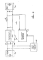
- FIG. 4 of the drawings there is shown a block diagram of a power conversion unit 10 constructed in accordance with the present invention. As was depicted in Fig. 1, the power conversion system interconnects a d.c. source 11 with the electric utility grid 13. A power flow control circuit 30 is also shown whose construction and function will be subsequently described. The power flow control circuit 30 is preferably included as part of the power conversion unit 10 and housed therewith.
- the power conversion unit 10 comprises a bidirectional switching mode amplifier 25, a coupling inductor 12 and a controlled feedback network 26.
- the amplifier 25 generates an output voltage V o in response to an input signal V, at terminal 27, the signal V, being generated by the controlled feedback network 26.
- Amplifier 25 is preferably a Class D, bidirectional switching mode amplifier of the type disclosed in U.S. Patent No. 4,020,361, which is hereby incorporated by reference.
- the amplifier 25 is controlled to have negative output resistance at the nominal frequency f o and positive output resistance at frequencies substantially different from the nominal frequency.
- the feedback network 26 is responsive to the voltage V G presented by the power grid and also to a signal V c from the power flow control circuit 30.
- Signal V c determines the power flow to the grid 13.
- Input signal V to the conversion unit 10 is generated by transforming the voltage V a in feedback network 26.
- Feedback network 26 has a transfer function, which will be subsequently described, and which is controlled, in part by the control voltage V C .
- V o is required to have certain amplitude and phase characteristics relative to V G at the nominal frequency f o of the grid 13 in order for current I to be injected into the grid at a desirable phase relationship toV G .
- d.c. power is taken from the array 11 and converted to a.c. power, the generated a.c. current I being in phase with V a .
- the current I may be desirable for the current I to be somewhat out of phase with Va in order to improve the overall load power factor seen by the grid 13. For simplicity's sake, however, the current I is shown in phase with V G in Fig. 2(a).
- V G and V O are preferentially as depicted in Fig. 2(b) so that, at these frequencies, the bidirectional amplifier 25 absorbs power from the grid 13. Because of the bidirectional nature of the switching mode amplifier 25, the latter a.c. power from the grid will be converted to d.c. power at the d.c. input 28 of the amplifier where it will be available to be reconverted into useful power at the nominal frequency f o and can be returned to the grid 13.
- the transfer function of the feedback circuit 26 is selected such that V O and V G have the relationship depicted in Fig. 2(a) for frequencies near the nominal frequency f. and the relationship depicted in Fig. 2(b) for frequencies significantly different from nominal frequency f o , e.g. at frequencies equal to or greater than twice the nominal frequency f o .
- Fig. 2(a) will change to show I lagging V G somewhat, and the transfer function of feedback network 26 will likewise change.
- V a control signal V which, when amplified by the amplifer 25 (Fig. 4), will provide a voltage V o having the desired relationship to V a at f o (as shown in Fig. 2(a)) and at frequencies equal to or greater than 2f o (as shown in Fig. 2(b)).
- Fig. 6 shows a detailed logic diagram of the power conversion unit 10.
- the transfer function depicted in Fig. 5 is embodied in the feedback network 26 shown in Fig. 6.
- the a.c. grid voltage of V G is input to the network 26 via a transformer 33 which reduces the voltage to a level (V G ') suitable for network 26.
- the feedback network 26 consists of three parallel path circuits 34, 35 and 36 which correspond to the transfer functions identified as 34', 35' and 36' in Fig. 5.
- the electrical outputs of the circuits 34, 35 and 36 are added at operational amplifier 38 in Fig. 6 which corresponds to the summing junction adder 38' in Fig. 5.
- resistor 37 determines the overall gain of the operational amplifier 38.
- the electrical output of the operational amplifier 38 provides the control input V, for the bidirectional switching mode amplifier 25.
- the first feedback path 34 of the network 26, consisting of a resistor 39, provides a signal which is in phase with the power grid voltage V G at all frequencies. If this were the only feedback path, V o would exactly track V G both in frequency and phase and no power transfer would occur between the grid and the switching mode amplifier 25.
- the second feedback path 35 includes a two- pole low-pass active filter comprising an operational amplifier 50 and appropriate circuit elements 45-49. Elements 45-49 are selected so that at the nominal frequency f o the amplitude is boosted significantly and the phase is shifted by 90°.
- Feedback path 35 also contains an electronic attenuator circuit 55 which corresponds to attenuator 55' shown in Fig. 5.
- the attenuator circuit 55 of Fig. 6 includes two field effect transistors 51 and 52 and a resistor 53.
- the drain to source resistance of the field effect transistor 51 is controlled by control voltage V c , the resistance increasing for increasingly negative values of V c .
- feedback path 35 when combined with feedback path 34, adjusts the phase of V o relative to V a so that electrical power transfer from the d.c. source 11 to the grid 13 at the nominal frequency f o will occur depending on the magnitude of control voltage Vc.
- Feedback path 36 in Fig. 6 includes an operational amplifier 40 with a feedback resistor 42 and an input resistor 41, all connected in series with a capacitor 43 and a resistor 44 at the output of the amplifier.
- Feedback path 36 generates a feedback signal component which lags the voltage V G by 90°. This signal component increases in amplitude proportionally with frequency until the frequency approaches: where R is the resistance of resistor 44 and C is the capacitance of capacitor 43.
- the lagging output voltage produced by feedback path 36 causes the bidirectional amplifier 25 to absorb power from the grid 13 at frequencies substantially above the nominal frequency f o .
- the power flow at the nominal frequency f o (i.e. 60 Hz) is controlled in response to control signal V c to the field effect transistor 51.
- the 90° lag component contributed by feedback path 36 produces a reverse power flow from the grid 13 through the switching mode amplifier 25 to the d.c. source 11.
- the leading 90° component produced by the feedback path 35 at the nominal frequency f o increases to exceed the component from path 36 and cause power at the nominal frequency to flow from the d.c. source 11 through the amplifier 25 to the grid 13.
- Fig. 6 also illustrates an embodiment of the power flow control circuit 30 which is preferably employed for a d.c. source having a substantial source impedance Z s such as a photovoltaic array. If the d.c. source has such a substantial source resistance, it may be desirable to maintain the voltage V DC at the input to the switching mode amplifier 25 at a substantially constant value.
- a Zener diode 60 in combination with a series resistor 58, provides a reference voltage to one input of an operational amplifier 59 in the control circuit 30.
- Resistor 58 is coupled to a convenient voltage supply (bias) appropriately provided in the conversion unit.
- V oc is applied through a voltage divider, comprising a pair of series resistors 56 and 57, to a second input of the operation amplifier 59.
- Operational amplifier 59 outputs the control signal V c to the feedback network 26.
- V c represents the difference between the solar array voltage and the desired solar array voltage.
- a non-zero value of V c causes a change in the power flow in such a manner as to reduce the value of V c , i.e. to return the array voltage to the desired voltage.
- the power may even be controlled so that power flows in the reverse direction, i.e. from the grid 13 to the power conversion unit 11. This reverse power flow could be sensed and used to initiate a turn-off of the power conversion unit utilizing the Start & Stop Controller 73 which is described below.
- V DC is also a function of other parameters affecting the alternative source, such as the temperature of the array. Accordingly, the power flow control circuit 30 may be modified, if desired, to effectively adjust the reference voltage as a function of the temperature of the photovoltaic array, or any other desired parameter.
- switching mode amplifier 25 includes four electronic power switches S,-S 4 , each of which may consist of several parallel transistors and a drive circuit. Across each electronic power switch S,-S 4 , is connected a corresponding diode D 1 -D 4 , repectively, which permits reactively generated currents to flow against the normal conduction paths through the switches.
- the power switches S l -S 4 are controlled by a control logic circuit 61 comprising a triangular wave generator 62, comparator amplifiers 63 and 64, logical invertors 65 and 66 and an inverting amplifier 67, all connected as shown in Fig. 6.
- the control logic circuit 61 is responsive to the output signal V, from the feedback network 26.
- the frequency of the triangular wave V T produced by the generator 62 is preferably selected to be at least several times the highest frequency to be found in the signal V,. While a frequency of 600 Hz for the triangular wave would likely be a sufficiently high frequency for 50 Hz or 60 Hz systems, it is in the audible range and a power conversion unit 10 so constructed may emit audible noise. To avoid the introduction of such audible noise, it is preferable to select the frequency of V T to be in the inaudible range, such as 20 KHz to 30 KHz or higher.
- Fig. 3 In order to protect the power conversion unit 10 against possible abnormal conditions on the grid, it is preferably provided with additional protection devices beyond the circuit breaker 17 shown in Fig. 3. These devices may include circuitry which monitors the frequency and voltage of V a and shuts down the unit 10 whenever the frequency and/or voltage of V G are outside their normally acceptable ranges.
- Such protective circuitry is represented by Over and Under Frequency Sampling Circuit 70, Over and Under Voltage Sampling Circuit 71, OR gate 72 and Start and Stop Controller 73.
- Monitoring Circuits 70 and 71 output a control signal whenever the frequency of voltage, respectively, of V G is unacceptable.
- the control signals are logically ORed by an OR gate 72, and the Controller 73 responds to the resulting output control signal from OR gate 72 by shutting down the unit 10 and disconnecting it from the power grid 13 by deactivating output contactor 74.
- Further protective devices may be provided, such as thermal switches, which may be used to shut down the unit 10 in response to unacceptably high temperatures in the cabinet housing the power conversion unit.
- the Start and Stop Controller 73 may also be responsive to the input source 11 to restart the power conversion unit when certain source conditions are attained, e.g. the source voltage is within a predetermined voltage range.
- the new and improved electrical power conversion system of the present invention is extremely reliable, efficient and easy to use and provides substantial improvements in operating performance over all known previous conversion systems.
- the conversion system provides a negative output resistance at the nominal frequency of the utility power grid and a positive output resistance at frequencies significantly different from the nominal frequency.
- the system of the present invention effectively provides power to the grid at the nominal frequency and absorbs useless power from the grid at other frequencies for conversion and return to the power grid at the desired nominal frequency.
Abstract
Description
- This invention relates generally to electrical power conversion and, more particularly, to new and improved electrical power conversion systems for use with alternative energy sources and which may be utilized to interconnect the alternative energy source with an a.c. power grid, such as the electrical power grid of an electric public utility or a local diesel generator system, so that the alternative energy source more effectively supplements the power grid.
- The electrical output from most alternative energy sources, such as photovoltaic arrays (solar cells), fuel cells, windmills, Stirling engines and other such sources, is not ideal. That is, the output energy provided by such sources is unregulated in voltage, and in the case of an alternating current (a.c.) output, the frequency is also unregulated. For most applications of alternative energy sources, some form of a power conversion, typically in the form of a conveniently packaged power conversion unit, is necessary to provide output power of the desired type (a.c. or d.c.) and quality.
- When a power conversion unit is to be used not only to convert the power to the appropriate type and quality, but also to interconnect the alternative energy source with an a.c. power grid, special problems are often encountered. The output power from the conversion unit must be high quality a.c., that is, have low harmonic current distortion and near-unity output power factor. The conversion unit must operate stably in multi-unit deployment (i.e. with many units connected to the same power grid) without "cross-talk", which could result in system oscillation. The conversion unit must be able to operate automatically with such non-ideal alternative energy sources, as photovoltaic (solar cell) arrays.
- In the prior art, two types of power converters have generally been used to operate between a direct current (d.c.) alternative energy source and an electric utility power grid. Line-commutated power conversion units use the utility voltage to control switching operations (in particular, the turn-off of the conduction states of switching devices such as thyristors used in the units). Self-commutated power conversion units, on the other hand, provide internal circuits for both the turn-on and turn-off of switching devices. The line-commutated power conversion units, while simpler in general than self-commutated power units, generally have very poor quality current waveforms and power factors. Additionally, line-commutated converters usually require large output filters to enhance the quality of the output current waveform. Such large output filters, besides adding cost to line-commutated power converter units, also increase the likelihood of electrical power grid oscillations occurring at certain frequencies.
- Self-commutated power conversion units generally have a better output waveform than line-commutated power converter units. Typically, such self-commutated converters use a phase-locked loop which synchronizes the units to the power grid, and therefore, are not capable of a fast response to perturbations on the power grid. Some units employ large output filters which are typically resonant with the grid at some frequencies.
- Both the line-commutated and the self-commutated power conversion systems tend to degrade the quality of the power on the electrical power grid by generating harmonics of the nominal operating frequency and generating other electrical noise. The line-commutated power converters further tend to degrade the quality of the grid by drawing reactive power from the grid. It may, in fact, be desirable for such power converters to supply reactive power to the grid to compensate for reactive loads on the grid. Electrical noise and harmonics are also undesirable on the power grid because, among other things, they can interfere with radio and television reception.
- Hence, those concerned with the development and use of electrical power conversion systems have long recognized the need for improved methods and apparatus for not only efficiently converting power from an alternative energy source to high-quality a.c. power utilizable by a power grid, but also for absorbing power from the utility at frequencies above or below the nominal operating frequency of the utility and converting such wasted power into useful power at the nominal frequency of the utility. The present invention clearly fulfills these needs.
- U.S. Patent No. 4,020,316 teaches a switching- mode amplifier which may be used to convert DC power at it's input to a.c. power at it's output. The amplifier may be controlled to handle relatively large dynamic ranges such as might be necessary when the output voltage corresponds to a music or voice signal.
- U.S. Patent No. 4,178,629 is concerned with an uninterruptable power supply of the type which may be used in computer installations. The power supply includes a d.c. to a.c. converter having wave shape control for decreasing distortion when powering reactive loads.
- The present invention provides a power conversion system for absorbing electrical power from a first power source and converting it to electrical power at the nominal or primary operating frequency of a second power source, and is characterized by circuits which absorb power from the second source at frequencies differing substantially from the nominal frequency and convert that additional power to power at the nominal frequency.
- In another aspect, the invention provides a method of electrical power conversion characterized by the steps of absorbing electrical power from an AC source of frequencies other than the nominal operating frequency of the source and converting the absorbed electrical power to additional electrical power at the nominal frequency of the AC source.
-
- Fig. 1 is a block diagram of an overall system, showing a power conversion unit in use in accordance with the invention;
- Figs. 2(a) and 2(b) are vector diagrams depicting the conversion unit and power grid phase relationships at frequencies around the nominal frequency of the grid and at frequencies significantly different from the nominal frequency of the grid, respectively;
- Fig. 3 is a combined block diagram and electrical schematic illustrating how an alternative energy source, such as a solar array, may be connected to the power grid via the power conversion unit;
- Fig. 4 is a block diagram of a presently preferred embodiment of a power conversion system according to the present invention;
- Fig. 5 is a block diagram of a presently preferred embodiment of the feedback network used in the power converter; and
- Fig. 6 is a more detailed block diagram and electrical schematic of a power conversion system, in accordance with the invention.
- Referring now to the drawings, and particularly to Fig. 1 thereof, a
power conversion unit 10 of the type described herein is shown coupling an alternative energy source, such as a d.c.source 11 topower grid 13. Thepower conversion unit 10 is shown connected to thepower grid 13 via aninductor 12, Normally, theinductor 12 is housed with theconversion unit 10 and is considered as a part thereof. However, for purposes of explanation, it is shown separately in Fig. 1 so that the output voltage Vo depicted in Fig. 1 may be appropriately defined. - The d.c.
source 11 may conceptually be considered as a d.c. potential source Vs in series with a source impedance Zs, where Vs may consist of an a.c. power source and appropriate rectifiers and filters to produce a d.c. voltage for input to thepower conversion unit 10. Thepower grid 13 may be conceptually considered as an a.c. potential source Vu in series with a source impedance Zu. The grid voltage VG sensed by theconversion unit 10 depends not only on the voltage Vu, but also on the impedance Zu. - The
alternative energy source 11 may be an array of photovoltaic cells (solar cells), a windmill and d.c. generator combination, a Stirling generator or any other appropriate source. In typical operation of thepower conversion unit 10, electrical power is extracted from the d.c.source 11 and injected into thepower grid 13 by generation of a current I in proper phase relation to the a.c. grid voltage VG, at the nominal operation frequency fo of the grid. Those skilled in the art will recognize, of course, that the nominal frequency fo of most domestic electric utilities is either 50 or 60 Hz. In certain specialized applications, electric power systems having other nominal frequencies are also known. The power conversion method and apparatus of the present . invention may be designed to work at any nominal frequency. - The voltage of the grid, VG, is composed of the desirable nominal frequency fo and also includes undesirable harmonics of the nominal frequency, grid noise and transients. The
conversion unit 10 of the present invention will not only convert the voltage Vs from the d.c.source 11 to an a.c. output voltage Vo at the nominal frequency of the utility, but also will absorb power from thegrid 13 at harmonics of the nominal frequency and at noise frequencies, convert the absorbed power to the nominal frequency f. and return it to the grid as useful power. Thus, theconversion unit 10 is capable of not only providing power to thegrid 13 from thesource 11, but can also improve the quality of power available from the grid, itself, by converting useless energy to useful form. - The
conversion unit 10 outputs an a.c. voltage Vo at the nominal frequency fo. For a positive flow of electrical power form thepower conversion unit 10 to theelectric utility grid 13 at the nominal frequency fo, the conversion unit provides the necessary phase shift and attenuation characteristics to provide the voltage vector relationships shown in Fig. 2(a) of the drawings. in this regard,V O must leadV G in phase. The phase angle between Vo andV G is φO and is diagrammatically defined in Fig. 2(a). A voltage VL, the voltage across theinductor 12, is also diagrammatically defined as being equal to Vo minus VG (those skilled in the art will recognize that the bar above these symbols indicated that they are being treated as vector quantities, consistent with their depiction in Fig. 2(a)). - Generally, it is desirable that the current I be injected into the
grid 13 in phase withV G. For this to occur, the output voltage Vo from theconversion unit 10 must have an appropriate amplitude and phase characteristic such thatV L leadsV G by 90°. The power flow P into thegrid 13 is generally defined as follows:
- For a unity power factor, that is the case where VL leads VG by 90°, equation (1) becomes:

- When VL does not lead VG by exactly 90°, the power from the
power conversion unit 10 to thepower grid 13 will have both real and reactive components at the nominal frequency fo. This is not necessarily undesirable, since, as is well known, reactive loads experienced by most power grids are inductive and appropriate selection of the reactive components of the power flow P can be used to make thepower conversion unit 10 appear as a capacitive load and thereby improve the overall power factor of the load on the grid. Thus, the power conversion system of the present invention may be used to improve the power factor of the load seen by the grid, if desired, by appropriately selecting the phase ofV L relative toV G. The manner in which the latter is accomplished will be subsequently described. - Turning now more particularly to Fig. 3 of the drawings, it is anticipated that the
power conversion unit 10 of the present invention will find particular use for interconnecting an array ofsolar cells 11, possibly disposed on the roof of a user's residence, to thelocal power grid 13 via adistribution panel 14 at the user's residence. Of course, thepower conversion unit 10 may be used in non-residential applications as well, such as office buildings and factories, and, as previously indicated may be powered fromsources 11 other than solar cells. - Fig. 3 schematically depicts how the
solar array 11 in thepower conversion unit 10 may be interconnected to thepower grid 13 via thedistribution panel 14. The photovoltaic or solar cell array provides direct current to thepower conversion unit 10 overlines 15. The electrical output of theconversion unit 10 is preferably coupled at thedistribution panel 14 viaelectric lines 16 andcircuit breaker 17 to the 240 volt a.c. mains 20 typically found in conventional distribution panels. These electrical mains are connected to thegrid 13 via circuit breakers 18 and akilowatt hour meter 19, both of which are typically located in or adjacent thepanel 14. Also connected to the mains 20 are a plurality ofseparate circuits 21 for using electrical energy at the user's residence. These circuits are usually interconnected to mains 20 viaindividual circuit breakers 22. - Of course, if no
array 11 norpower conversion unit 10 are provided, electrical energy is merely drawn off thepower grid 13 by thecircuits 21 and the amount of power used is reported by thekilowatt hour meter 19. However, when anarray 11 andpower conversion unit 10 are used, they can provide electrical energy to thecircuits 21, and, in the event thearray 11 andpower conversion unit 10 have more energy available than is needed at any given time by thecircuits 21, they can pump electrical energy back through themeter 19 to thepower grid 13 for use by other customers of the grid. Themeter 19 in this case increments as energy is consumed by the user from the power grid 13 (i.e.circuits 21 are consuming more energy than thearray 11 andpower conversion unit 10 are supplying) and decrements as energy is pumped into thegrid 13 by the user (i.e.circuits 21 are consuming less energy than thearray 11 andpower conversion unit 10 are generating). - It will be apparent to those skilled in the art that, if a
conventional meter 19 is used, the user is credited for the generation of power at the same rate as the user-is charged for the consumption of electric power. That is, if the user is charged $0.10 for each kilowatt hour used, he or she is also automatically credited $0.10 for each kilowatt hour generated. It may well be however, that the utility will be required by rate fixing authorities to charge for electric consumption at one rate and credit for electric power generation at another rate. In this event, special metering techniques will be required to correctly record the charges and credits. Such metering techniques are outside the scope of the present invention, and, accordingly, are not described here. - Referring now to Fig. 4 of the drawings, there is shown a block diagram of a
power conversion unit 10 constructed in accordance with the present invention. As was depicted in Fig. 1, the power conversion system interconnects a d.c.source 11 with theelectric utility grid 13. A powerflow control circuit 30 is also shown whose construction and function will be subsequently described. The powerflow control circuit 30 is preferably included as part of thepower conversion unit 10 and housed therewith. - The
power conversion unit 10 comprises a bidirectionalswitching mode amplifier 25, acoupling inductor 12 and a controlledfeedback network 26. Theamplifier 25 generates an output voltage Vo in response to an input signal V, atterminal 27, the signal V, being generated by the controlledfeedback network 26. -
Amplifier 25 is preferably a Class D, bidirectional switching mode amplifier of the type disclosed in U.S. Patent No. 4,020,361, which is hereby incorporated by reference. In accordance with the invention, theamplifier 25 is controlled to have negative output resistance at the nominal frequency fo and positive output resistance at frequencies substantially different from the nominal frequency. - The
feedback network 26 is responsive to the voltage VG presented by the power grid and also to a signal Vc from the powerflow control circuit 30. Signal Vc determines the power flow to thegrid 13. - Input signal V, to the
conversion unit 10 is generated by transforming the voltage Va infeedback network 26.Feedback network 26 has a transfer function, which will be subsequently described, and which is controlled, in part by the control voltage VC. - Referring again to Fig. 2(a), it will be recalled that Vo is required to have certain amplitude and phase characteristics relative to
V G at the nominal frequency fo of thegrid 13 in order for current I to be injected into the grid at a desirable phase relationship toVG. With the relationship shown in Fig. 2(a), d.c. power is taken from thearray 11 and converted to a.c. power, the generated a.c. current I being in phase with Va. In some applications it may be desirable for the current I to be somewhat out of phase with Va in order to improve the overall load power factor seen by thegrid 13. For simplicity's sake, however, the current I is shown in phase with VG in Fig. 2(a). - At grid frequencies significantly different from the nominal frequency fo, e.g. at frequencies equal to or greater than 2fo, where undesirable grid harmonics and noise are found, the relationship between VG and
V O is preferentially as depicted in Fig. 2(b) so that, at these frequencies, thebidirectional amplifier 25 absorbs power from thegrid 13. Because of the bidirectional nature of the switchingmode amplifier 25, the latter a.c. power from the grid will be converted to d.c. power at the d.c.input 28 of the amplifier where it will be available to be reconverted into useful power at the nominal frequency fo and can be returned to thegrid 13. - The transfer function of the
feedback circuit 26 is selected such thatV O andV G have the relationship depicted in Fig. 2(a) for frequencies near the nominal frequency f. and the relationship depicted in Fig. 2(b) for frequencies significantly different from nominal frequency fo, e.g. at frequencies equal to or greater than twice the nominal frequency fo. Of course, if it is desired that theconversion unit 10 have a capacitive component to its output impedance, then Fig. 2(a) will change to show I lagging VG somewhat, and the transfer function offeedback network 26 will likewise change. The transfer function of thefeedback control network 26 depicted in Fig. 5 (expressed in Laplace transforms) will generate a control signal V, which, when amplified by the amplifer 25 (Fig. 4), will provide a voltage Vo having the desired relationship to Va at fo (as shown in Fig. 2(a)) and at frequencies equal to or greater than 2fo (as shown in Fig. 2(b)). - Fig. 6 shows a detailed logic diagram of the
power conversion unit 10. The transfer function depicted in Fig. 5 is embodied in thefeedback network 26 shown in Fig. 6. The a.c. grid voltage of VG is input to thenetwork 26 via atransformer 33 which reduces the voltage to a level (VG') suitable fornetwork 26. - The
feedback network 26 consists of threeparallel path circuits circuits operational amplifier 38 in Fig. 6 which corresponds to the summing junction adder 38' in Fig. 5. Those skilled in the art will recognize thatresistor 37 determines the overall gain of theoperational amplifier 38. The electrical output of theoperational amplifier 38 provides the control input V, for the bidirectionalswitching mode amplifier 25. - The
first feedback path 34 of thenetwork 26, consisting of aresistor 39, provides a signal which is in phase with the power grid voltage VG at all frequencies. If this were the only feedback path, Vo would exactly track VG both in frequency and phase and no power transfer would occur between the grid and the switchingmode amplifier 25. - The
second feedback path 35 includes a two- pole low-pass active filter comprising an operational amplifier 50 and appropriate circuit elements 45-49. Elements 45-49 are selected so that at the nominal frequency fo the amplitude is boosted significantly and the phase is shifted by 90°. -
Feedback path 35 also contains anelectronic attenuator circuit 55 which corresponds to attenuator 55' shown in Fig. 5. Theattenuator circuit 55 of Fig. 6 includes twofield effect transistors 51 and 52 and aresistor 53. The drain to source resistance of the field effect transistor 51 is controlled by control voltage Vc, the resistance increasing for increasingly negative values of Vc. It will be apparent to those skilled in the art, thatfeedback path 35, when combined withfeedback path 34, adjusts the phase of Vo relative to Va so that electrical power transfer from the d.c.source 11 to thegrid 13 at the nominal frequency fo will occur depending on the magnitude of control voltage Vc. -
Feedback path 36 in Fig. 6 includes an operational amplifier 40 with afeedback resistor 42 and an input resistor 41, all connected in series with a capacitor 43 and aresistor 44 at the output of the amplifier.Feedback path 36 generates a feedback signal component which lags the voltageV G by 90°. This signal component increases in amplitude proportionally with frequency until the frequency approaches:
resistor 44 and C is the capacitance of capacitor 43. The lagging output voltage produced byfeedback path 36 causes thebidirectional amplifier 25 to absorb power from thegrid 13 at frequencies substantially above the nominal frequency fo. - The power flow at the nominal frequency fo (i.e. 60 Hz) is controlled in response to control signal Vc to the field effect transistor 51. When the transistor 51 is "off", the 90° lag component contributed by
feedback path 36 produces a reverse power flow from thegrid 13 through the switchingmode amplifier 25 to the d.c.source 11. As the conductance of the transistor 51 increases, the leading 90° component produced by thefeedback path 35 at the nominal frequency fo increases to exceed the component frompath 36 and cause power at the nominal frequency to flow from the d.c.source 11 through theamplifier 25 to thegrid 13. - Fig. 6 also illustrates an embodiment of the power
flow control circuit 30 which is preferably employed for a d.c. source having a substantial source impedance Zs such as a photovoltaic array. If the d.c. source has such a substantial source resistance, it may be desirable to maintain the voltage VDC at the input to the switchingmode amplifier 25 at a substantially constant value. AZener diode 60, in combination with aseries resistor 58, provides a reference voltage to one input of anoperational amplifier 59 in thecontrol circuit 30.Resistor 58 is coupled to a convenient voltage supply (bias) appropriately provided in the conversion unit. Voc is applied through a voltage divider, comprising a pair ofseries resistors 56 and 57, to a second input of theoperation amplifier 59.Operational amplifier 59 outputs the control signal Vc to thefeedback network 26. - Vc represents the difference between the solar array voltage and the desired solar array voltage. A non-zero value of Vc causes a change in the power flow in such a manner as to reduce the value of Vc, i.e. to return the array voltage to the desired voltage. In the instance where the power available from the array at that voltage is insufficient to support electrical losses within the power conversion unit, the power may even be controlled so that power flows in the reverse direction, i.e. from the
grid 13 to thepower conversion unit 11. This reverse power flow could be sensed and used to initiate a turn-off of the power conversion unit utilizing the Start & Stop Controller 73 which is described below. - The optimum value of VDC is also a function of other parameters affecting the alternative source, such as the temperature of the array. Accordingly, the power
flow control circuit 30 may be modified, if desired, to effectively adjust the reference voltage as a function of the temperature of the photovoltaic array, or any other desired parameter. - Turning now to the switching
mode amplifier 25, U.S. Patent No. 4,020,361 includes a detailed discussion of the switching mode amplifier and, therefore, it is only briefly described here. As depicted in Fig. 6, switchingmode amplifier 25 includes four electronic power switches S,-S4, each of which may consist of several parallel transistors and a drive circuit. Across each electronic power switch S,-S4, is connected a corresponding diode D1-D4, repectively, which permits reactively generated currents to flow against the normal conduction paths through the switches. - The power switches Sl-S4 are controlled by a control logic circuit 61 comprising a triangular wave generator 62,
comparator amplifiers 63 and 64,logical invertors amplifier 67, all connected as shown in Fig. 6. The control logic circuit 61 is responsive to the output signal V, from thefeedback network 26. - The frequency of the triangular wave VT produced by the generator 62 is preferably selected to be at least several times the highest frequency to be found in the signal V,. While a frequency of 600 Hz for the triangular wave would likely be a sufficiently high frequency for 50 Hz or 60 Hz systems, it is in the audible range and a
power conversion unit 10 so constructed may emit audible noise. To avoid the introduction of such audible noise, it is preferable to select the frequency of VT to be in the inaudible range, such as 20 KHz to 30 KHz or higher. - In order to protect the
power conversion unit 10 against possible abnormal conditions on the grid, it is preferably provided with additional protection devices beyond thecircuit breaker 17 shown in Fig. 3. These devices may include circuitry which monitors the frequency and voltage of Va and shuts down theunit 10 whenever the frequency and/or voltage of VG are outside their normally acceptable ranges. In Fig. 6 such protective circuitry is represented by Over and UnderFrequency Sampling Circuit 70, Over and Under Voltage Sampling Circuit 71, OR gate 72 and Start and Stop Controller 73. -
Monitoring Circuits 70 and 71 output a control signal whenever the frequency of voltage, respectively, of VG is unacceptable. The control signals are logically ORed by an OR gate 72, and the Controller 73 responds to the resulting output control signal from OR gate 72 by shutting down theunit 10 and disconnecting it from thepower grid 13 by deactivating output contactor 74. Further protective devices may be provided, such as thermal switches, which may be used to shut down theunit 10 in response to unacceptably high temperatures in the cabinet housing the power conversion unit. - The Start and Stop Controller 73 may also be responsive to the
input source 11 to restart the power conversion unit when certain source conditions are attained, e.g. the source voltage is within a predetermined voltage range. - The new and improved electrical power conversion system of the present invention is extremely reliable, efficient and easy to use and provides substantial improvements in operating performance over all known previous conversion systems. The conversion system provides a negative output resistance at the nominal frequency of the utility power grid and a positive output resistance at frequencies significantly different from the nominal frequency. Hence, the system of the present invention effectively provides power to the grid at the nominal frequency and absorbs useless power from the grid at other frequencies for conversion and return to the power grid at the desired nominal frequency.
- Having described the invention in connection with a preferred embodiment thereof, it will be apparent that various modifications may be made. For example, those practicing the present invention may well desire to add additional elements such as electromagnetic interference input and output filters, or input storage capacitors.
Claims (10)
Priority Applications (1)
| Application Number | Priority Date | Filing Date | Title |
|---|---|---|---|
| AT82306817T ATE19909T1 (en) | 1981-12-21 | 1982-12-20 | METHOD AND DEVICE FOR TRANSFORMING ELECTRICAL POWER. |
Applications Claiming Priority (2)
| Application Number | Priority Date | Filing Date | Title |
|---|---|---|---|
| US33307081A | 1981-12-21 | 1981-12-21 | |
| US333070 | 1981-12-21 |
Publications (2)
| Publication Number | Publication Date |
|---|---|
| EP0085249A1 EP0085249A1 (en) | 1983-08-10 |
| EP0085249B1 true EP0085249B1 (en) | 1986-05-21 |
Family
ID=23301134
Family Applications (1)
| Application Number | Title | Priority Date | Filing Date |
|---|---|---|---|
| EP82306817A Expired EP0085249B1 (en) | 1981-12-21 | 1982-12-20 | Method and apparatus for electrical power conversion |
Country Status (12)
| Country | Link |
|---|---|
| EP (1) | EP0085249B1 (en) |
| JP (1) | JPS58119776A (en) |
| AT (1) | ATE19909T1 (en) |
| AU (1) | AU9173682A (en) |
| CA (1) | CA1210809A (en) |
| DE (1) | DE3271279D1 (en) |
| DK (1) | DK562582A (en) |
| IL (1) | IL67534A0 (en) |
| MX (1) | MX154860A (en) |
| NO (1) | NO824277L (en) |
| NZ (1) | NZ202841A (en) |
| ZA (1) | ZA829316B (en) |
Cited By (2)
| Publication number | Priority date | Publication date | Assignee | Title |
|---|---|---|---|---|
| DE9107538U1 (en) * | 1991-06-19 | 1992-10-15 | Peters, Helmut, 2854 Loxstedt, De | |
| EP2856598B1 (en) * | 2012-06-01 | 2023-07-19 | The University of Hong Kong | Input ac voltage control bi-directional power converters |
Families Citing this family (4)
| Publication number | Priority date | Publication date | Assignee | Title |
|---|---|---|---|---|
| GB2189097A (en) * | 1986-04-07 | 1987-10-14 | Powamate Ltd | Solar power systems |
| US6809942B2 (en) * | 2001-06-29 | 2004-10-26 | Sanyo Electric Co., Ltd. | System interconnection electric power generator and control method therefor |
| JP5773191B2 (en) * | 2011-05-31 | 2015-09-02 | オムロン株式会社 | Detection apparatus and method, and program |
| CN110571826B (en) * | 2019-09-18 | 2023-02-21 | 河南柏科沃电子科技有限公司 | Pile up formula reactive power compensation system |
Family Cites Families (3)
| Publication number | Priority date | Publication date | Assignee | Title |
|---|---|---|---|---|
| US4020361A (en) * | 1974-10-04 | 1977-04-26 | Delta Electronic Control Corporation | Switching mode power controller of large dynamic range |
| US3946242A (en) * | 1975-03-03 | 1976-03-23 | Wilkerson A W | Geophysical energy source utilization circuit |
| US4178629A (en) * | 1977-02-28 | 1979-12-11 | International Business Machines Corporation | D. C. Powered A. C. supply for reactive loads |
-
1982
- 1982-12-17 NZ NZ202841A patent/NZ202841A/en unknown
- 1982-12-20 DE DE8282306817T patent/DE3271279D1/en not_active Expired
- 1982-12-20 AT AT82306817T patent/ATE19909T1/en not_active IP Right Cessation
- 1982-12-20 CA CA000418118A patent/CA1210809A/en not_active Expired
- 1982-12-20 JP JP57222183A patent/JPS58119776A/en active Pending
- 1982-12-20 DK DK562582A patent/DK562582A/en not_active Application Discontinuation
- 1982-12-20 ZA ZA829316A patent/ZA829316B/en unknown
- 1982-12-20 NO NO824277A patent/NO824277L/en unknown
- 1982-12-20 EP EP82306817A patent/EP0085249B1/en not_active Expired
- 1982-12-21 IL IL67534A patent/IL67534A0/en unknown
- 1982-12-21 AU AU91736/82A patent/AU9173682A/en not_active Abandoned
-
1983
- 1983-01-03 MX MX195763A patent/MX154860A/en unknown
Cited By (2)
| Publication number | Priority date | Publication date | Assignee | Title |
|---|---|---|---|---|
| DE9107538U1 (en) * | 1991-06-19 | 1992-10-15 | Peters, Helmut, 2854 Loxstedt, De | |
| EP2856598B1 (en) * | 2012-06-01 | 2023-07-19 | The University of Hong Kong | Input ac voltage control bi-directional power converters |
Also Published As
| Publication number | Publication date |
|---|---|
| JPS58119776A (en) | 1983-07-16 |
| IL67534A0 (en) | 1983-05-15 |
| ATE19909T1 (en) | 1986-06-15 |
| DK562582A (en) | 1983-08-03 |
| ZA829316B (en) | 1983-10-26 |
| MX154860A (en) | 1987-12-22 |
| EP0085249A1 (en) | 1983-08-10 |
| CA1210809A (en) | 1986-09-02 |
| NO824277L (en) | 1983-06-22 |
| NZ202841A (en) | 1986-03-14 |
| DE3271279D1 (en) | 1986-06-26 |
| AU9173682A (en) | 1983-06-30 |
Similar Documents
| Publication | Publication Date | Title |
|---|---|---|
| Saxena et al. | Implementation of a grid-integrated PV-battery system for residential and electrical vehicle applications | |
| US7145266B2 (en) | Parallel-connected inverters with separate controllers having impedance current regulators | |
| US5017800A (en) | AC to DC to AC power conversion apparatus with few active switches and input and output control | |
| Vilathgamuwa et al. | Protection of microgrids during utility voltage sags | |
| Chakraborty et al. | Experimental evaluation of active filtering in a single-phase high-frequency AC microgrid | |
| WO1996018937A1 (en) | Grid connected bi-directional converter including a pwm, dc-dc chopper, and energy storage/supply device | |
| WO2006136801A2 (en) | Improvements in electrical power converters | |
| JP4494562B2 (en) | Power converter for photovoltaic power generation | |
| Hatziadoniu et al. | A power conditioner for a grid-connected photovoltaic generator based on the 3-level inverter | |
| Lin et al. | Plug-and-play control of the virtual infinite capacitor | |
| Ismail et al. | A multi-objective control scheme of a voltage source converter with battery–supercapacitor energy storage system used for power quality improvement | |
| Itoh et al. | Experimental verification of single-phase inverter with power decoupling function using boost-up chopper | |
| EP0085249B1 (en) | Method and apparatus for electrical power conversion | |
| Choi et al. | Transformerless line-interactive UPS with low ground leakage current | |
| Boegli et al. | Realization of a new inverter circuit for direct photovoltaic energy feedback into the public grid | |
| Tom et al. | Solid state transformer for wind power interfacing | |
| CN110880766A (en) | Voltage drop compensation device and method based on unified power quality controller | |
| Ali et al. | Mixed AC/DC system stability under uncertainty | |
| Tayab et al. | A modified droop controller for parallel operation of single-phase inverters in Islanded microgrid | |
| Gow et al. | Novel fast-acting predictive current mode controller for power electronic converters | |
| Wang et al. | Parallel operation of solid state transformer | |
| Han et al. | Hybrid-mode cuk inverter with low-voltage ride-through capability under grid-faults | |
| Sapara et al. | Current unbalance and DC bus unbalance control for three level grid tied NPC inverter fed by DER with DC-DC boost converter | |
| Roncero-Clemente et al. | Grid-connected single-phase 3L-T-type qZS inverter for renewable energy | |
| Makdisie et al. | Applied Power Electronics: Inverters, UPSs |
Legal Events
| Date | Code | Title | Description |
|---|---|---|---|
| PUAI | Public reference made under article 153(3) epc to a published international application that has entered the european phase |
Free format text: ORIGINAL CODE: 0009012 |
|
| AK | Designated contracting states |
Designated state(s): AT BE CH DE FR GB IT LI LU NL SE |
|
| 17P | Request for examination filed |
Effective date: 19831213 |
|
| GRAA | (expected) grant |
Free format text: ORIGINAL CODE: 0009210 |
|
| AK | Designated contracting states |
Kind code of ref document: B1 Designated state(s): AT BE CH DE FR GB IT LI LU NL SE |
|
| PG25 | Lapsed in a contracting state [announced via postgrant information from national office to epo] |
Ref country code: NL Effective date: 19860521 Ref country code: LI Effective date: 19860521 Ref country code: IT Free format text: LAPSE BECAUSE OF FAILURE TO SUBMIT A TRANSLATION OF THE DESCRIPTION OR TO PAY THE FEE WITHIN THE PRESCRIBED TIME-LIMIT;WARNING: LAPSES OF ITALIAN PATENTS WITH EFFECTIVE DATE BEFORE 2007 MAY HAVE OCCURRED AT ANY TIME BEFORE 2007. THE CORRECT EFFECTIVE DATE MAY BE DIFFERENT FROM THE ONE RECORDED. Effective date: 19860521 Ref country code: FR Free format text: THE PATENT HAS BEEN ANNULLED BY A DECISION OF A NATIONAL AUTHORITY Effective date: 19860521 Ref country code: CH Effective date: 19860521 Ref country code: BE Effective date: 19860521 Ref country code: AT Effective date: 19860521 |
|
| REF | Corresponds to: |
Ref document number: 19909 Country of ref document: AT Date of ref document: 19860615 Kind code of ref document: T |
|
| PG25 | Lapsed in a contracting state [announced via postgrant information from national office to epo] |
Ref country code: SE Effective date: 19860531 |
|
| REF | Corresponds to: |
Ref document number: 3271279 Country of ref document: DE Date of ref document: 19860626 |
|
| REG | Reference to a national code |
Ref country code: CH Ref legal event code: PL |
|
| NLV1 | Nl: lapsed or annulled due to failure to fulfill the requirements of art. 29p and 29m of the patents act | ||
| EN | Fr: translation not filed | ||
| PG25 | Lapsed in a contracting state [announced via postgrant information from national office to epo] |
Ref country code: LU Free format text: LAPSE BECAUSE OF NON-PAYMENT OF DUE FEES Effective date: 19861231 |
|
| PLBE | No opposition filed within time limit |
Free format text: ORIGINAL CODE: 0009261 |
|
| STAA | Information on the status of an ep patent application or granted ep patent |
Free format text: STATUS: NO OPPOSITION FILED WITHIN TIME LIMIT |
|
| 26N | No opposition filed | ||
| PGFP | Annual fee paid to national office [announced via postgrant information from national office to epo] |
Ref country code: GB Payment date: 19891130 Year of fee payment: 8 |
|
| PGFP | Annual fee paid to national office [announced via postgrant information from national office to epo] |
Ref country code: DE Payment date: 19891221 Year of fee payment: 8 |
|
| PG25 | Lapsed in a contracting state [announced via postgrant information from national office to epo] |
Ref country code: GB Effective date: 19901220 |
|
| GBPC | Gb: european patent ceased through non-payment of renewal fee | ||
| PG25 | Lapsed in a contracting state [announced via postgrant information from national office to epo] |
Ref country code: DE Effective date: 19910903 |