EP0035710B1 - Direct current actuating circuit - Google Patents
Direct current actuating circuit Download PDFInfo
- Publication number
- EP0035710B1 EP0035710B1 EP81101417A EP81101417A EP0035710B1 EP 0035710 B1 EP0035710 B1 EP 0035710B1 EP 81101417 A EP81101417 A EP 81101417A EP 81101417 A EP81101417 A EP 81101417A EP 0035710 B1 EP0035710 B1 EP 0035710B1
- Authority
- EP
- European Patent Office
- Prior art keywords
- valve
- load
- swinging
- gate device
- capacitor
- Prior art date
- Legal status (The legal status is an assumption and is not a legal conclusion. Google has not performed a legal analysis and makes no representation as to the accuracy of the status listed.)
- Expired
Links
Images
Classifications
-
- H—ELECTRICITY
- H02—GENERATION; CONVERSION OR DISTRIBUTION OF ELECTRIC POWER
- H02M—APPARATUS FOR CONVERSION BETWEEN AC AND AC, BETWEEN AC AND DC, OR BETWEEN DC AND DC, AND FOR USE WITH MAINS OR SIMILAR POWER SUPPLY SYSTEMS; CONVERSION OF DC OR AC INPUT POWER INTO SURGE OUTPUT POWER; CONTROL OR REGULATION THEREOF
- H02M3/00—Conversion of dc power input into dc power output
- H02M3/02—Conversion of dc power input into dc power output without intermediate conversion into ac
- H02M3/04—Conversion of dc power input into dc power output without intermediate conversion into ac by static converters
- H02M3/10—Conversion of dc power input into dc power output without intermediate conversion into ac by static converters using discharge tubes with control electrode or semiconductor devices with control electrode
- H02M3/125—Conversion of dc power input into dc power output without intermediate conversion into ac by static converters using discharge tubes with control electrode or semiconductor devices with control electrode using devices of a thyratron or thyristor type requiring extinguishing means
- H02M3/135—Conversion of dc power input into dc power output without intermediate conversion into ac by static converters using discharge tubes with control electrode or semiconductor devices with control electrode using devices of a thyratron or thyristor type requiring extinguishing means using semiconductor devices only
Definitions
- the invention relates to a DC control circuit with the features listed in the preamble of claim 1.
- a DC regulator circuit is known from German Offenlegungsschrift 2622351.
- the voltage of a given DC voltage source can be reduced in such a way that the mean value of the input voltage for a connected load can be controlled down to almost zero.
- This average is primarily dependent on the duty cycle of the main valve. Due to the necessary swinging of the charge of the commutation capacitor, the minimum switch-on times of the main valve cannot be fallen below.
- the voltage of the commutation capacitor is applied to the load in addition to the input voltage.
- the commutation capacitor In the normal control range, the commutation capacitor is left in the polarity between the extinction and re-ignition of the main valve, which polarity it has assumed due to the current commutated on the extinguishing branch during the extinguishing process.
- This state of the commutation capacitor is maintained even after the main valve has been ignited and only at a point in time coordinated with the dimensions of the swinging choke and the commutation capacitor before the intended ignition of the commutation valve (quenching valve) is the polarity of the capacitor reversed by firing the reversing valve and the circuit for quenching the main valve prepared.
- the extinguishing valve and the return valve are ignited simultaneously.
- the duty cycle of the main valve is reduced by shortening the time interval between the ignition times of the main valve and the reversing valve until both ignition times coincide.
- the main valve no longer receives any ignition pulses.
- the output voltage arises from the fact that in the time interval between the ignition of the return valve and the end of the return process (extinction of the return valve) the commutation valve is energized and thus a superposition of the voltage of the DC voltage source and the voltage on the commutation capacitor is applied to the load.
- the reduction in the output voltage thus occurs in that the ignition timing for the commutation valve, which is to be placed in the current carrying time of the return valve (which can also be a diode), is delayed and is shifted to the extinction time of the return valve. This reduces the section of the capacitor voltage to be placed on the load.
- the invention has for its object to provide a DC chopper, the output voltage is extended over the range that can be achieved by controlling the main valve duty cycle and in which an overload of the commutation capacitor is kept low without using a recharging branch.
- a common inductance can be used as a return choke and a changeover choke, which is connected upstream of an anti-parallel connection of the changeover valve and the return valve.
- This inductance and the commutation capacitor thus form a resonant circuit for swinging around and swinging back, in which the swinging back valve and the swinging around valve lie.
- this inductance is divided into two parts, one part being formed by a further choke which is arranged in the connecting line between the commutation capacitor and the one terminal of the load.
- the two free-wheeling diodes connect the two choke ends to the connecting line coming from the other load connection, so that this part of the resonant circuit inductance is short-circuited in operating states in which both free-wheeling diodes are conductive at the same time.
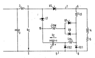
- the terminals 1 of a DC voltage source, their inductance 2 and their capacitance 3 are shown symbolically: In particular, this can be a DC voltage supply network with a downstream input inductance and a smoothing capacitor.
- the consumer is symbolized by an inductor 4 with an ohmic component 5.
- the input terminal 6 is connected via a line 7 to one pole of the DC voltage source, the other load input 8 via a line 9 to the other pole of the DC voltage source.
- line 7 is the controllable main valve of the DC controller circuit, which is designed as a thyristor HT.
- the two connections of the main valve HT are through an extinguishing branch. connected with each other.
- the extinguishing branch consists of a controllable commutation valve which is poled parallel to the main valve and which serves as an extinguishing valve in the normal control range and is also designed as a thyristor LT.
- a commutation capacitor C is connected downstream of this commutation valve LT.
- One electrode of the commutation valve LT is therefore connected to an output of the DC voltage source together with an electrode of the main valve HT, the other electrode of the commutation valve LT is connected via capacitor C to the other electrode of the main valve and the load input 6.
- a swinging branch Parallel to the commutation capacitor is a swinging branch which is formed from a controllable swinging valve (swinging thyristor UT) and a swinging choke.
- This swing branch is in series with the combutation valve LT, ie it leads from the connection point between LT and C to the load input 6.
- the swing valve UT is polarized in the direction of current flow of the commutation valve LT.
- a return oscillation branch which contains a return oscillation valve with an upstream return oscillation choke which is polarized opposite to the direction of current flow of the commutation valve.
- the return valve can be a thyristor, but it can also be designed as a return diode RD. It is advantageous to use only one common throttle Lsw as the oscillating choke and swinging choke; In this case, the valves UT and RD are connected in anti-parallel and are located in series with the throttle L sw in the connecting line between points 10 and 6.
- a first freewheel valve (diode FD1) is arranged parallel to the load 4, 5.
- the arrangement of these components corresponds to the known circuits, but a reloading branch corresponding to the known arrangements is dispensed with.
- the arrangement can be supplemented by a protective inductance L LS for the valves HT and FD1 if the input inductance 2 is not sufficient for this. Care must be taken to ensure that this protective inductance lies outside the current path which is formed by the elements 2, LT, C, FD2 and the line 9.
- the circuit is supplemented by a further choke L ss , which is connected downstream of the connection of the commutation capacitor C leading to the load input 6 within the part of the quenching arm which is parallel to the resonant circuit, and by a second free-wheeling valve which connects the voltage source 1 to the other load input 8 leading connecting line with the load-side connection of the commutation capacitor C connects.
- This second one-way valve FD2 is poled in parallel to the first one-way valve FD1. If both valves are live, they release a line for bridging the other throttle L ss .
- the energy originally stored in the capacitor C is stored in the inductance in order to be fed back into the capacitor during the oscillation.
- the voltage returns to its original value after a sinusoidal oscillation. If the commutation valve LT is now ignited during this oscillation, the oscillating circuit is connected to the voltage of the voltage source until the free-wheeling valve FD1 extinguishes and thus there is a short-term increase in current through the commutation capacitor C.
- the oscillating circuit energy is thus increased briefly when LT is ignited. After the end of the swing back, the capacitor is therefore charged more than before the start of the swing.
- the capacitor voltage thus increases with each ignition pulse and is ultimately only limited by the ohmic resistances of the circuit. However, these should be kept low with a view to high efficiency.
- the FD2 cathode becomes negative with respect to the FD1 cathode, so that FD1 blocks and FD2 takes over the load current.
- the current commutates from FD2 to FD1.
- This commutation is relatively slow, so that Lss is short-circuited for a while and the resonant circuit inductance is only formed by L sw .
- the capacitor voltage also rises more slowly, which corresponds to a reduction in the energy in the resonant circuit.
- This energy reduction is caused by the fact that the energy to be dissipated is stored outside the resonant circuit, namely in the inductance L ss , without ohmic losses occurring. It can be achieved by optimizing the throttle dimensions that just as much energy is withdrawn from the resonant circuit as is supplied after the commutation valve has been ignited. This results in a minimal capacitor overload where J A is the load current. This overload was only 10% of the DC input voltage in a first laboratory system, while it was 60% in a same system without a second freewheeling diode. Furthermore, most valves are stressed less because of the voltage division at the chokes L sw and Lss. The quenching voltage peak in the output voltage is also reduced, by 50% in the aforementioned laboratory system. The consequence of this is that not only can a reloading branch be dispensed with, but the other components can also be designed for a lower maximum load.
- the optimal division of the resonant circuit inductance into the inductances L ss and L sw results from a consideration of the resonant circuit.
- the resonant circuit damping can be detected by parameter h, which represents the ratio of the capacitor voltage 0 before ignition of the return valve to the capacitor voltage U i8o ° after half the period of oscillation .
Landscapes
- Engineering & Computer Science (AREA)
- Power Engineering (AREA)
- Dc-Dc Converters (AREA)
- Lock And Its Accessories (AREA)
- Control Of Electrical Variables (AREA)
- Ignition Installations For Internal Combustion Engines (AREA)
- Power Conversion In General (AREA)
Abstract
Description
Die Erfindung betrifft eine Gleichstromstellerschaltung mit den im Oberbegriff des Anspruchs 1 aufgeführten Merkmalen. Eine derartige Gleichstromstellerschaltung ist aus der deutschen Offenlegungsschrift 2622351 bekannt.The invention relates to a DC control circuit with the features listed in the preamble of
Mit einer herkömmlichen Stellerschaltung kann die Spannung einer vorgegebenen Gleichspannungsquelle so herabgesetzt werden, daß der Mittelwert der Eingangsspannung für eine angeschlossene Last bis nahe an den Wert Null herabgesteuert werden kann. Dieser Mittelwert ist in erster Linie abhängig von der Einschaltdauer des Hauptventils. Bedingt durch das erforderliche Umschwingen der Ladung des Kommutierungskondensators können dabei gewisse Mindesteinschaltdauern des Hauptventils nicht unterschritten werden. Während des Löschvorganges wird die Spannung des Kommutierungskondensators zusätzlich zur Eingangsspannung an die Last gelegt. Folglich können im normalen Steuerbereich, in dem die Eingangsspannung der Last (d. h. die Ausgangsspannung der Schaltung) durch die Einschaltdauer des Hauptventils gesteuert wird, nur Mindestspannungen von etwa 8 bis 12% der Eingangsgleichspannung erreicht werden.With a conventional actuator circuit, the voltage of a given DC voltage source can be reduced in such a way that the mean value of the input voltage for a connected load can be controlled down to almost zero. This average is primarily dependent on the duty cycle of the main valve. Due to the necessary swinging of the charge of the commutation capacitor, the minimum switch-on times of the main valve cannot be fallen below. During the quenching process, the voltage of the commutation capacitor is applied to the load in addition to the input voltage. As a result, in the normal control range where the input voltage of the load (i.e. the output voltage of the circuit) is controlled by the duty cycle of the main valve, only minimum voltages of about 8 to 12% of the DC input voltage can be achieved.
In der erwähnten deutschen Offenlegungsschrift 2 622 351 ist daher vorgesehen, diesen normalen Steuerbereich durch einen weiteren Bereich für kleine Ausgangsspannungen zu ergänzen: Das Hauptventil bleibt gesperrt und durch eine entsprechende Steuerung des Kommutierungsventils, des Umschwingventils und des ebenfalls steuerbar ausgeführten Rückschwingventils wird an die Last nur ein bestimmter Ausschnitt der Kondensatorspannung während des Umschwingvorganges gelegt (»Anschnittsteuerung«). Gegenüber herkömmlichen Gleichstromstellerschaltungen zeichnet sich die Schaltung durch die Polarität des Umschwingventils und des Rückschwingventils aus.In the aforementioned German published patent application 2 622 351, it is therefore provided that this normal control range be supplemented by a further range for low output voltages: the main valve remains blocked and the load is only applied to the load by appropriate control of the commutation valve, the reversing valve and the reversing valve, which is also controllable a certain section of the capacitor voltage is placed during the reversal process ("gate control"). Compared to conventional direct current regulator circuits, the circuit is distinguished by the polarity of the reversing valve and the return valve.
Im normalen Steuerbereich ist vorgesehen, den Kommutierungskondensator in der Zeit zwischen Erlöschen und Wiederzünden des Hauptventils.in der Polarität zu belassen, die er durch den während des Löschvorganges auf den Löschzweig kommutierten Strom angenommen hat. Dieser Zustand des Kommutierungskondensators wird auch nach Zündung des Hauptventils beibehalten und erst zu einem auf die Dimensionierungen der Umschwingdrossel und des Kommutierungskondensators abgestimmten Zeitpunkt vor dem vorgesehenen Zünden des Kommutierungsventils (Löschventils) wird durch Zünden des Umschwingventils die Kondensatorladung umgepolt und die Schaltung für die Löschung des Hauptventils vorbereitet. Die Zündung von Löschventil und Rückschwingventil erfolgt-gleichzeitig. Zur Verkleinerung der Ausgangsspannung wird die Einschaltdauer des Hauptventils durch Verkürzung des Zeitabstandes zwischen den Zündzeitpunkten von Hauptventil und Umschwingventil verringert, bis beide Zündzeitpunkte zusammenfallen.In the normal control range, the commutation capacitor is left in the polarity between the extinction and re-ignition of the main valve, which polarity it has assumed due to the current commutated on the extinguishing branch during the extinguishing process. This state of the commutation capacitor is maintained even after the main valve has been ignited and only at a point in time coordinated with the dimensions of the swinging choke and the commutation capacitor before the intended ignition of the commutation valve (quenching valve) is the polarity of the capacitor reversed by firing the reversing valve and the circuit for quenching the main valve prepared. The extinguishing valve and the return valve are ignited simultaneously. To reduce the output voltage, the duty cycle of the main valve is reduced by shortening the time interval between the ignition times of the main valve and the reversing valve until both ignition times coincide.
Zur weiteren Verkleinerung der Eingangsspannung wird nun auf die »Anschnittssteuerung« übergegangen, bei der das Hauptventil keine Zündimpulse mehr erhält. Die Ausgangsspannung entsteht dadurch, daß im Zeitintervall zwischen der Zündung des Rückschwingventils und dem Ende des Rückschwingvorganges (Erlöschen des Rückschwingventils) das Kommutierungsventil stromführend ist und somit an die Last eine Überlagerung der Spannung der Gleichspannungsquelle und der Spannung am Kommutierungskondensator gelegt ist. Die Verkleinerung der Ausgangsspannung geschieht also dadurch, daß der Zündzeitpunkt für das Kommutierungsventil, der in die Stromführungsdauer des Rückschwingventils (das auch eine Diode sein kann) zu legen ist, verzögert wird und zum Löschzeitpunkt des Rückschwingventils verschoben wird. Dadurch wird der an die Last zu legende Ausschnitt der Kondensatorspannung verkleinert.To further reduce the input voltage, we now switch to the "gate control", in which the main valve no longer receives any ignition pulses. The output voltage arises from the fact that in the time interval between the ignition of the return valve and the end of the return process (extinction of the return valve) the commutation valve is energized and thus a superposition of the voltage of the DC voltage source and the voltage on the commutation capacitor is applied to the load. The reduction in the output voltage thus occurs in that the ignition timing for the commutation valve, which is to be placed in the current carrying time of the return valve (which can also be a diode), is delayed and is shifted to the extinction time of the return valve. This reduces the section of the capacitor voltage to be placed on the load.
Es hat sich aber gezeigt, daß insbesondere bei einem Betrieb im Anschnittssteuerbereich eine erhebliche Überladung des Kondensators über die zum Löschen des Hauptthyristors nötige Spannung auftritt. Da die Ventile und Drosseln auf den maximalen Umschwingstrom und die maximale Sperrspannung ausgelegt werden müssen, sollen derartige Überspannungen verhindert werden. Daher ist in der erwähnten Offenlegungsschrift vorgesehen, antiparallel zum Kommutierungsventil ein Ladeventil mit vorgeschaltetem ohmschen Widerstand zu schalten, durch den die Überladung teilweise in die Gleichspannungsquelle zurückgespeist, teilweise in Wärme umgesetzt wird. Um zu verhindern, daß im normalen Steuerbereich bei gezündetem Hauptventil der Kondensator über den Rückladezweig teilweise entladen wird und die Kondensatorladung nicht mehr zur Löschung des Hauptventils ausreicht, ist in der deutschen Offenlegungsschrift 2 635 953 eine veränderte Impulsfolge für den Hauptsteuerbereich angegeben, bei der das Umschwingventil jeweils kurz vor dem Hauptventil gezündet wird.However, it has been shown that, particularly when operating in the gate control region, the capacitor is considerably overcharged beyond the voltage required to quench the main thyristor. Such overvoltages should be prevented since the valves and chokes have to be designed for the maximum reversing current and the maximum reverse voltage. Therefore, it is provided in the above-mentioned laid-open publication to switch a charging valve with an upstream ohmic resistance in antiparallel to the commutation valve, through which the overload is partly fed back into the DC voltage source and partly converted into heat. In order to prevent the condenser from being partially discharged via the return branch in the normal control area when the main valve is ignited and the condenser charge no longer being sufficient to extinguish the main valve, a modified pulse sequence for the main control area is specified in the German Offenlegungsschrift 2,635,953, in which the reversing valve is ignited shortly before the main valve.
Derartige Anordnungen haben aber den Nachteil, daß sie wegen des Rückladezweiges einen hohen Material- und Platzbedarf sowie wegen der ohmschen Widerstände einen geringeren Wirkungsgrad aufweisen.Such arrangements have the disadvantage, however, that they have a high material and space requirement due to the reloading branch and a lower efficiency because of the ohmic resistors.
Der Erfindung liegt die Aufgabe zugrunde, einen Gleichstromsteller anzugeben, dessen Ausgangsspannung über den Bereich, der durch die Steuerung der Hauptventil-Einschaltdauer erreichbar ist, erweitert ist und bei dem eine Überladung des Kommutierungskondensators ohne Verwendung eines Rückladezweiges gering gehalten wird.The invention has for its object to provide a DC chopper, the output voltage is extended over the range that can be achieved by controlling the main valve duty cycle and in which an overload of the commutation capacitor is kept low without using a recharging branch.
Gemäß der Erfindung wird diese Aufgabe gelöst durch eine Schaltung mit den im Anspruch 1 angegebenen Merkmalen.According to the invention, this object is achieved by a circuit with the features specified in
Wie bereits bei bekannten Schaltungen kann als Rückschwingdrossel und Umschwingdrossel eine gemeinsame Induktivität verwendet werden, die einer Antiparallelschaltung von Umschwingventil und Rückschwingventil vorgeschaltet ist. Diese Induktivität und der Kommutierungskondensator bilden somit zum Umschwingen und Rückschwingen einen Schwingkreis, in dem das Rückschwingventil bzw. das Umschwingventil liegen. Gemäß der Erfindung ist diese Induktivität jedoch in zwei Teile aufgeteilt, wobei der eine Teil von einer weiteren Drossel gebildet wird, die in die Verbindungsleitung zwischen dem Kommutierungskondensator und dem einen Anschluß der Last angeordnet ist. Die beiden Freilaufdioden verbinden die beiden Drosselenden mit der vom anderen Lastanschluß kommenden Verbindungsleitung, so daß dieser Teil der Schwingkreisinduktivität bei Betriebszuständen kurzgeschlossen ist, bei denen beide Freilaufdioden gleichzeitig leitend sind.As in known circuits, a common inductance can be used as a return choke and a changeover choke, which is connected upstream of an anti-parallel connection of the changeover valve and the return valve. This inductance and the commutation capacitor thus form a resonant circuit for swinging around and swinging back, in which the swinging back valve and the swinging around valve lie. According to the invention, however, this inductance is divided into two parts, one part being formed by a further choke which is arranged in the connecting line between the commutation capacitor and the one terminal of the load. The two free-wheeling diodes connect the two choke ends to the connecting line coming from the other load connection, so that this part of the resonant circuit inductance is short-circuited in operating states in which both free-wheeling diodes are conductive at the same time.
Die Erläuterung der Erfindung und weiterer vorteilhafter Ausgestaltungen wird anhand einer Figur und eines bevorzugten Ausführungsbeispiels näher erläutert.The explanation of the invention and further advantageous embodiments is explained in more detail with reference to a figure and a preferred embodiment.
In der Figur sind die Klemmen 1 einer Gleichspannungsquelle, deren Induktivität 2 und deren Kapazität 3 symbolisch dargestellt: Insbesondere kann es sich hierbei um ein Gleichspannungsversorgungsnetz mit einer nachgeschalteten Eingangsinduktivität und einem Glättungskondensator handeln. Der Verbraucher ist durch eine Induktivität 4 mit ohmschen Anteil 5, symbolisiert. Die Eingangsklemme 6 ist über eine Leitung 7 mit dem einen Pol der Gleichspannungsquelle, der andere Lasteingang 8 über eine Leitung 9 mit dem anderen Pol der Gleichspannungsquelle verbunden. In der Leitung 7 liegt das steuerbare Hauptventil der Gleichstromstellerschaltung, das als Thyristor HT ausgeführt ist. Die beiden Anschlüsse des Hauptventils HT sind durch einen Löschzweig. miteinander verbunden. Der Löschzweig besteht aus einem steuerbaren, parallel zum Hauptventil gepolten Kommutierungsventil, das im normalen Steuerbereich als Löschventil dient und ebenfalls als Thyristor LT ausgeführt ist. Diesem Kommutierungsventil LT ist lastseitig ein Kommutierungskondensator C nachgeschaltet. Die eine Elektrode des. Kommutierungsventils LT ist also zusammen mit einer Elektrode des Hauptventils HT an einen Ausgang der Gleichspannungsquelle angeschlossen, die andere Elektrode des Kommutierungsventils LT ist über den Kondensator C mit der anderen Elektrode des Hauptventils und dem Lasteingang 6 verbunden. Parallel zum Kommutierungskondensator liegt ein Umschwingzweig, der aus einem steuerbaren Umschwingventil (Umschwingthyristor UT) und einer Umschwingdrossel gebildet wird. Dieser Umschwingzweig liegt in Reihe mit dem Kammutierungsventil LT, d. h. er führt vom Verbindungspunkt zwischen LT und C zum Lasteingang 6. Das Umschwingventil UT ist in Stromflußrichtung des Kommutierungsventils LT gepolt. Ebenfalls parallel zum Kommutierungskondensator und in Reihe mit dem Kommutierungsventil ist ein Rückschwingzweig angeordnet, der ein entgegengesetzt zur Stromflußrichtung des Kommutierungsventils gepoltes Rückschwingventil mitvorgeschalteter Rückschwingdrossel enthält. Das Rückschwingventil kann ein Thyristor sein, es kann aber auch als Rückschwingdiode RD ausgeführt sein. Vorteilhaft ist es, als Rückschwingdrossel und Umschwingdrossel nur eine gemeinsame Drossel Lsw zu verwenden; in diesem Fall sind die Ventile UT und RD antiparallel geschaltet und liegen gemeinsam in Reihe mit der Drossel Lsw in der Verbindungsleitung zwischen den Punkten 10 und 6.In the figure, the
Ferner ist parallel zur Last 4, 5 ein erstes Freilaufventil (Diode FD1) angeordnet. Die Anordnung dieser Bauteile entspricht den bekannten Schaltungen, wobei jedoch auf einen Rückladezweig entsprechend den bekannten Anordnungen verzichtet ist. Ferner kann die Anordnung durch eine Schutzinduktivität LLS für die-Ventile HT und FD1 ergänzt werden, falls die Eingangsinduktivität 2 hierzu nicht ausreicht. Dabei ist darauf zu achten, daß diese Schutzinduktivität außerhalb des Strompfades, der von den Elementen 2, LT, C, FD2 und der Leitung 9 gebildetwird, liegt.Furthermore, a first freewheel valve (diode FD1) is arranged parallel to the load 4, 5. The arrangement of these components corresponds to the known circuits, but a reloading branch corresponding to the known arrangements is dispensed with. Furthermore, the arrangement can be supplemented by a protective inductance L LS for the valves HT and FD1 if the input inductance 2 is not sufficient for this. Care must be taken to ensure that this protective inductance lies outside the current path which is formed by the elements 2, LT, C, FD2 and the line 9.
Gemäß der Erfindung wird die Schaltung ergänzt durch eine weitere Drossel Lss, die innerhalb des zum Rückschwingkreis parallelen Teiles des Löschzweiges dem zum Lasteingang 6 führenden Anschluß des Kommutierungskondensators C nachgeschaltet ist, und durch ein zweites Freilaufventil, das die von der Spannungsquelle 1 zum anderen Lasteingang 8 führende Verbindungsleitung mit dem lastseitigen Anschluß des Kommutierungskondensators C verbindet. Dieses zweite Freilaufventil FD2 ist parallel zum ersten Freilaufventil FD1 gepolt. Falls beide Ventile stromführend sind, geben sie also eine Leitung zur Überbrückung der weiteren Drossel Lss frei.According to the invention, the circuit is supplemented by a further choke L ss , which is connected downstream of the connection of the commutation capacitor C leading to the
Dieser Schaltung liegen Erkenntnisse über die Ursache einer Kondensatorüberladung zugrunde, die im folgenden für den Anschnittssteuerbereich (HT bleibt gesperrt) und den Fall, daß FD2 wie bei den bekannten Anordnungen nicht vorhanden ist, summarisch zusammengefaßt werden.This circuit is based on findings on the cause of capacitor overload, which are summarized below for the gate control area (HT remains blocked) and the case that FD2 is not present, as in the known arrangements.
Bei gesperrtem Kommutierungsventil LT führt FD1 den gesamten Laststrom und die Spannung Uc am Kommutierungskondensator C besitzt die negative, in Klammern angegebene Polarität. Durch Zünden des Umschwingventils UT schwingt die Kondensatorladung um, anschließend wird RD leitend und die Kondensatorladung schwingt wieder zurück. Es liegt also ein vom Kondensator C und einer SchwinginduktivitätWhen the commutation valve LT is blocked, FD1 carries the entire load current and the voltage U c at the commutation capacitor C has the negative polarity indicated in brackets. By igniting the reversing valve UT, the capacitor charge swings, then RD becomes conductive and the capacitor charge swings back again. So there is a capacitor C and an inductor
![]()
![]()
Durch die Erfindung soll nun dem Schwingkreis während des Umschwingens und Rückschwingens Energie entzogen werden, um die bei der nachfolgenden Zündung des Kommutierungsventils LT zufließende Energie zu kompensieren. Dies wird erreicht durch die Aufspaltung der Schwingkreisinduktivität in die beiden Teildrosseln Lsw und Lss, wobei die Drossel Lss durch die geschilderte Anordnung der beiden Freilaufventile FD1 und FD2 überbrückbar ist.By means of the invention, energy is now to be extracted from the resonant circuit during the swinging and swinging back, in order to compensate for the energy flowing in during the subsequent ignition of the commutation valve LT. This is achieved by splitting the resonant circuit inductance into the two partial chokes L sw and L ss , the choke L ss being able to be bridged by the arrangement of the two free-wheeling valves FD1 and FD2 described.
Durch Zünden des Umschwingventils UT wird nämlich die FD2-Kathode gegenüber der FD1-Kathode negativ, so daß FD1 sperrt und FD2 den Laststrom übernimmt. Beim anschließenden Nulldurchgang der Kondensatorspannung kommutiert der Strom von FD2 auf FD1. Diese Kommutierung verläuft verhältnismäßig langsam, so daß Lss eine Zeit lang kurzgeschlossen und die Schwingkreisinduktivität nur von Lsw gebildet wird. Infolgedessen steigt auch die Kondensatorspannung langsamer an, was einer Verminderung der Energie im Schwingkreis entspricht. Diese Energieverminderung wird dadurch hervorgerufen, daß die abzuführende Energie außerhalb des Schwingkreises, nämlich in der Induktivität Lss, gespeichert wird, ohne daß hierbei ohmsche Verluste auftreten. Dabei kann durch Optimierung der Drosseldimensionen erreicht werden, daß dem Schwingkreis gerade so viel Energie entzogen wird, als nach Zünden des Kommutierungsventils zugeführt wird. Es ergibt sich dann eine minimale Kondensatorüberladung![]()
![]()
Die optimale Aufteilung der Schwingkreisinduktivität in die Induktivitäten Lss und Lsw ergibt sich aus einer Betrachtung des Schwingkreises. Für den Schwingkreis kann die Schwingkreisdämpfung durch den Parameter h erfaßt werden, der das Verhältnis der Kondensatorspannung 0 vor Zünden des Rückschwingventils zur Kondensatorspannung Ui8o° nach halber Schwingdauer darstellt. Eine Viertelperiode nach Zünden des Umschwingventils tritt der maximale Umschwingstrom 1 auf. Mit den Größen![]()
![]()
![]()
![]()
![]()
![]()
![]()
![]()
Die Einhaltung dieser Dimensionierung erweist sich nicht als kritisch, so daß auch Abweichungen von 20% und darüber möglich sind.Adherence to this dimensioning does not prove to be critical, so that deviations of 20% and above are also possible.
Claims (2)
characterised by
Priority Applications (1)
| Application Number | Priority Date | Filing Date | Title |
|---|---|---|---|
| AT81101417T ATE6111T1 (en) | 1980-03-07 | 1981-02-26 | DC CONTROLLER CIRCUIT. |
Applications Claiming Priority (2)
| Application Number | Priority Date | Filing Date | Title |
|---|---|---|---|
| DE3008907 | 1980-03-07 | ||
| DE19803008907 DE3008907A1 (en) | 1980-03-07 | 1980-03-07 | DC CONTROLLER CIRCUIT |
Publications (3)
| Publication Number | Publication Date |
|---|---|
| EP0035710A2 EP0035710A2 (en) | 1981-09-16 |
| EP0035710A3 EP0035710A3 (en) | 1982-03-03 |
| EP0035710B1 true EP0035710B1 (en) | 1984-02-01 |
Family
ID=6096597
Family Applications (1)
| Application Number | Title | Priority Date | Filing Date |
|---|---|---|---|
| EP81101417A Expired EP0035710B1 (en) | 1980-03-07 | 1981-02-26 | Direct current actuating circuit |
Country Status (5)
| Country | Link |
|---|---|
| US (1) | US4358811A (en) |
| EP (1) | EP0035710B1 (en) |
| JP (1) | JPS56139076A (en) |
| AT (1) | ATE6111T1 (en) |
| DE (2) | DE3008907A1 (en) |
Families Citing this family (4)
| Publication number | Priority date | Publication date | Assignee | Title |
|---|---|---|---|---|
| US4394724A (en) * | 1981-10-30 | 1983-07-19 | Westinghouse Electric Corp. | Propulsion motor control apparatus and method |
| GB8402629D0 (en) * | 1984-02-01 | 1984-03-07 | Mcewan P M | Circuit breakers |
| ES2071730T3 (en) * | 1990-12-10 | 1995-07-01 | Asea Brown Boveri | PROCEDURE AND DEVICE FOR THE ELIMINATION OR REDUCTION OF HARMONICS AND / OR OF RESONANCE OSCILLATIONS. |
| EP0489947B1 (en) * | 1990-12-10 | 1995-03-22 | Asea Brown Boveri Ag | Turn-off circuit |
Family Cites Families (6)
| Publication number | Priority date | Publication date | Assignee | Title |
|---|---|---|---|---|
| US3414797A (en) * | 1966-05-20 | 1968-12-03 | Gen Electric | Power converter employing integrated magnetics |
| GB1239734A (en) * | 1969-01-13 | 1971-07-21 | ||
| BE775787A (en) * | 1971-11-25 | 1972-05-25 | Acec | ELECTRONIC DEVICE FOR ADJUSTING A DIRECT CURRENT. |
| FR2320658A1 (en) * | 1975-08-07 | 1977-03-04 | Jeumont Schneider | IMPROVEMENT IN CONSTANT FREQUENCY CURRENT CHIPS THAT ARE LIKELY TO SUPPLY AN INDUCTIVE LOAD AT LOW FLOW |
| FR2345760A1 (en) * | 1976-03-26 | 1977-10-21 | Cem Oerlikon Traction | DIRECT CURRENT REGULATOR |
| DE2831752A1 (en) * | 1978-07-19 | 1980-01-31 | Siemens Ag | CONVERTER WITH A DC INTERMEDIATE CIRCUIT |
-
1980
- 1980-03-07 DE DE19803008907 patent/DE3008907A1/en not_active Withdrawn
-
1981
- 1981-02-26 EP EP81101417A patent/EP0035710B1/en not_active Expired
- 1981-02-26 DE DE8181101417T patent/DE3162073D1/en not_active Expired
- 1981-02-26 AT AT81101417T patent/ATE6111T1/en not_active IP Right Cessation
- 1981-03-03 US US06/239,977 patent/US4358811A/en not_active Expired - Fee Related
- 1981-03-06 JP JP3236081A patent/JPS56139076A/en active Pending
Also Published As
| Publication number | Publication date |
|---|---|
| JPS56139076A (en) | 1981-10-30 |
| ATE6111T1 (en) | 1984-02-15 |
| DE3008907A1 (en) | 1981-09-17 |
| EP0035710A3 (en) | 1982-03-03 |
| EP0035710A2 (en) | 1981-09-16 |
| DE3162073D1 (en) | 1984-03-08 |
| US4358811A (en) | 1982-11-09 |
Similar Documents
| Publication | Publication Date | Title |
|---|---|---|
| DE102006029475A1 (en) | Power factor correction rectifier`s boost switching converter, has inrush control device for controlling bidirectional semiconductor switches, and for controlling control switch to turn one semiconductor switch on and off | |
| DE3734989A1 (en) | DC CIRCUIT BREAKER AND METHOD FOR COMMUTING IT | |
| DE2320128C3 (en) | Chopper | |
| DE2936063A1 (en) | DIMMING CIRCUIT | |
| DE1293323B (en) | Circuit arrangement for controlling the voltage of a consumer connected to a direct current source via a thyristor | |
| DE2639944A1 (en) | DC VOLTAGE CONVERTER | |
| DE1763411C3 (en) | Thyristor converter arrangement | |
| DE4421249C2 (en) | Switching power supply unit with snubber circuit | |
| DE2644715C2 (en) | Device for relieving electrical or electronic one-way switches from high power dissipation during switch-on - in which a non-zero current previously flowing in a different circuit path changes to the relevant one-way switch - and from excessive blocking voltage stress at the end of switch-off | |
| DE2357925A1 (en) | CIRCUIT TO LIMIT THE CHARGE CURRENT RISE | |
| EP2992598A1 (en) | Step-up or step-down converter comprising a bypass capacitor | |
| DE3405793A1 (en) | METHOD AND DEVICE FOR SHORT CIRCUIT PROTECTION OF A CONVERTER WITH GTO THYRISTORS | |
| EP0035710B1 (en) | Direct current actuating circuit | |
| DE2348952B2 (en) | COMMUTATION DEVICE FOR A DC CHOPPER CIRCUIT | |
| DE1638311A1 (en) | Circuit with controllable rectifiers | |
| EP0009225B1 (en) | Protective circuit | |
| DE2716367C2 (en) | Protective circuit for transistors working in alternating mode against inductive loads | |
| DE1638962A1 (en) | Circuit with controllable rectifiers | |
| DE2541687C3 (en) | Inverter and procedure for its operation | |
| DE3612524C2 (en) | ||
| DE3049020C2 (en) | Controllable DC / DC converter for power switch-mode power supplies | |
| DE3717488C2 (en) | ||
| DE2632785C3 (en) | DC chopper | |
| DE3815471C2 (en) | Low-loss wiring on at least one valve that can be switched off | |
| EP0539902A2 (en) | Switch-off snubber for A DC-DC converter |
Legal Events
| Date | Code | Title | Description |
|---|---|---|---|
| PUAI | Public reference made under article 153(3) epc to a published international application that has entered the european phase |
Free format text: ORIGINAL CODE: 0009012 |
|
| AK | Designated contracting states |
Designated state(s): AT CH DE |
|
| PUAL | Search report despatched |
Free format text: ORIGINAL CODE: 0009013 |
|
| 17P | Request for examination filed |
Effective date: 19811028 |
|
| AK | Designated contracting states |
Designated state(s): AT CH DE |
|
| GRAA | (expected) grant |
Free format text: ORIGINAL CODE: 0009210 |
|
| AK | Designated contracting states |
Designated state(s): AT CH DE LI |
|
| REF | Corresponds to: |
Ref document number: 6111 Country of ref document: AT Date of ref document: 19840215 Kind code of ref document: T |
|
| REF | Corresponds to: |
Ref document number: 3162073 Country of ref document: DE Date of ref document: 19840308 |
|
| PGFP | Annual fee paid to national office [announced via postgrant information from national office to epo] |
Ref country code: DE Payment date: 19840329 Year of fee payment: 4 |
|
| PGFP | Annual fee paid to national office [announced via postgrant information from national office to epo] |
Ref country code: CH Payment date: 19840524 Year of fee payment: 4 |
|
| PLBE | No opposition filed within time limit |
Free format text: ORIGINAL CODE: 0009261 |
|
| STAA | Information on the status of an ep patent application or granted ep patent |
Free format text: STATUS: NO OPPOSITION FILED WITHIN TIME LIMIT |
|
| 26N | No opposition filed | ||
| PGFP | Annual fee paid to national office [announced via postgrant information from national office to epo] |
Ref country code: AT Payment date: 19870128 Year of fee payment: 7 |
|
| PG25 | Lapsed in a contracting state [announced via postgrant information from national office to epo] |
Ref country code: AT Effective date: 19890226 |
|
| PG25 | Lapsed in a contracting state [announced via postgrant information from national office to epo] |
Ref country code: LI Effective date: 19890228 Ref country code: CH Effective date: 19890228 |
|
| REG | Reference to a national code |
Ref country code: CH Ref legal event code: PL |
|
| PG25 | Lapsed in a contracting state [announced via postgrant information from national office to epo] |
Ref country code: DE Effective date: 19891101 |