DE112011102970T5 - Nanostructured electrode for pseudo-capacitive energy storage - Google Patents
Nanostructured electrode for pseudo-capacitive energy storage Download PDFInfo
- Publication number
- DE112011102970T5 DE112011102970T5 DE112011102970T DE112011102970T DE112011102970T5 DE 112011102970 T5 DE112011102970 T5 DE 112011102970T5 DE 112011102970 T DE112011102970 T DE 112011102970T DE 112011102970 T DE112011102970 T DE 112011102970T DE 112011102970 T5 DE112011102970 T5 DE 112011102970T5
- Authority
- DE
- Germany
- Prior art keywords
- pseudocapacitive
- pseudo
- capacitive
- energy storage
- substrate
- Prior art date
- Legal status (The legal status is an assumption and is not a legal conclusion. Google has not performed a legal analysis and makes no representation as to the accuracy of the status listed.)
- Pending
Links
- 238000004146 energy storage Methods 0.000 title claims description 37
- 239000000463 material Substances 0.000 claims abstract description 173
- 239000000758 substrate Substances 0.000 claims abstract description 112
- 238000000231 atomic layer deposition Methods 0.000 claims abstract description 17
- 238000000034 method Methods 0.000 claims description 50
- PNEYBMLMFCGWSK-UHFFFAOYSA-N aluminium oxide Inorganic materials [O-2].[O-2].[O-2].[Al+3].[Al+3] PNEYBMLMFCGWSK-UHFFFAOYSA-N 0.000 claims description 16
- 238000000151 deposition Methods 0.000 claims description 12
- 238000000576 coating method Methods 0.000 claims description 11
- 239000011248 coating agent Substances 0.000 claims description 10
- 125000000524 functional group Chemical group 0.000 claims description 7
- 239000004020 conductor Substances 0.000 claims description 5
- 239000008151 electrolyte solution Substances 0.000 claims description 4
- AMWRITDGCCNYAT-UHFFFAOYSA-L hydroxy(oxo)manganese;manganese Chemical compound [Mn].O[Mn]=O.O[Mn]=O AMWRITDGCCNYAT-UHFFFAOYSA-L 0.000 claims description 4
- 150000002500 ions Chemical class 0.000 claims description 4
- 229910000480 nickel oxide Inorganic materials 0.000 claims description 3
- 238000004519 manufacturing process Methods 0.000 claims description 2
- GNRSAWUEBMWBQH-UHFFFAOYSA-N oxonickel Chemical compound [Ni]=O GNRSAWUEBMWBQH-UHFFFAOYSA-N 0.000 claims description 2
- WOCIAKWEIIZHES-UHFFFAOYSA-N ruthenium(iv) oxide Chemical compound O=[Ru]=O WOCIAKWEIIZHES-UHFFFAOYSA-N 0.000 claims description 2
- 229910001925 ruthenium oxide Inorganic materials 0.000 claims 1
- 239000012876 carrier material Substances 0.000 abstract description 32
- 239000002071 nanotube Substances 0.000 abstract description 8
- TWNQGVIAIRXVLR-UHFFFAOYSA-N oxo(oxoalumanyloxy)alumane Chemical compound O=[Al]O[Al]=O TWNQGVIAIRXVLR-UHFFFAOYSA-N 0.000 abstract description 6
- 239000003990 capacitor Substances 0.000 abstract description 5
- 238000005137 deposition process Methods 0.000 abstract description 3
- 238000004070 electrodeposition Methods 0.000 abstract description 3
- 238000000277 atomic layer chemical vapour deposition Methods 0.000 abstract description 2
- 230000006911 nucleation Effects 0.000 abstract description 2
- 238000010899 nucleation Methods 0.000 abstract description 2
- 239000010410 layer Substances 0.000 description 79
- 230000008569 process Effects 0.000 description 28
- OKTJSMMVPCPJKN-UHFFFAOYSA-N Carbon Chemical compound [C] OKTJSMMVPCPJKN-UHFFFAOYSA-N 0.000 description 15
- 239000011148 porous material Substances 0.000 description 15
- 229910052751 metal Inorganic materials 0.000 description 12
- 239000002184 metal Substances 0.000 description 12
- 239000000376 reactant Substances 0.000 description 9
- 235000004522 Pentaglottis sempervirens Nutrition 0.000 description 8
- 230000008021 deposition Effects 0.000 description 8
- 229910044991 metal oxide Inorganic materials 0.000 description 8
- 150000004706 metal oxides Chemical class 0.000 description 8
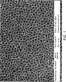
- 238000001878 scanning electron micrograph Methods 0.000 description 8
- 239000002356 single layer Substances 0.000 description 8
- 239000003792 electrolyte Substances 0.000 description 7
- 238000002679 ablation Methods 0.000 description 6
- 239000000126 substance Substances 0.000 description 6
- 238000006243 chemical reaction Methods 0.000 description 5
- 238000005229 chemical vapour deposition Methods 0.000 description 5
- 230000007704 transition Effects 0.000 description 5
- 238000002048 anodisation reaction Methods 0.000 description 4
- 230000015572 biosynthetic process Effects 0.000 description 4
- 238000005530 etching Methods 0.000 description 4
- MYMOFIZGZYHOMD-UHFFFAOYSA-N Dioxygen Chemical compound O=O MYMOFIZGZYHOMD-UHFFFAOYSA-N 0.000 description 3
- 229920002472 Starch Polymers 0.000 description 3
- 239000000853 adhesive Substances 0.000 description 3
- 230000001070 adhesive effect Effects 0.000 description 3
- 229910052782 aluminium Inorganic materials 0.000 description 3
- XAGFODPZIPBFFR-UHFFFAOYSA-N aluminium Chemical compound [Al] XAGFODPZIPBFFR-UHFFFAOYSA-N 0.000 description 3
- 229910052799 carbon Inorganic materials 0.000 description 3
- 229910001882 dioxygen Inorganic materials 0.000 description 3
- 150000002739 metals Chemical class 0.000 description 3
- 238000006479 redox reaction Methods 0.000 description 3
- 235000019698 starch Nutrition 0.000 description 3
- 238000003860 storage Methods 0.000 description 3
- 229910001218 Gallium arsenide Inorganic materials 0.000 description 2
- 240000004050 Pentaglottis sempervirens Species 0.000 description 2
- NBIIXXVUZAFLBC-UHFFFAOYSA-N Phosphoric acid Chemical compound OP(O)(O)=O NBIIXXVUZAFLBC-UHFFFAOYSA-N 0.000 description 2
- QAOWNCQODCNURD-UHFFFAOYSA-N Sulfuric acid Chemical compound OS(O)(=O)=O QAOWNCQODCNURD-UHFFFAOYSA-N 0.000 description 2
- 239000002253 acid Substances 0.000 description 2
- 238000007743 anodising Methods 0.000 description 2
- 230000002547 anomalous effect Effects 0.000 description 2
- QVGXLLKOCUKJST-UHFFFAOYSA-N atomic oxygen Chemical compound [O] QVGXLLKOCUKJST-UHFFFAOYSA-N 0.000 description 2
- 230000000694 effects Effects 0.000 description 2
- 230000005684 electric field Effects 0.000 description 2
- 238000009713 electroplating Methods 0.000 description 2
- 239000007789 gas Substances 0.000 description 2
- 238000000227 grinding Methods 0.000 description 2
- 239000011810 insulating material Substances 0.000 description 2
- 239000012212 insulator Substances 0.000 description 2
- 239000000203 mixture Substances 0.000 description 2
- 238000012986 modification Methods 0.000 description 2
- 230000004048 modification Effects 0.000 description 2
- 230000003647 oxidation Effects 0.000 description 2
- 238000007254 oxidation reaction Methods 0.000 description 2
- 229910052760 oxygen Inorganic materials 0.000 description 2
- 239000001301 oxygen Substances 0.000 description 2
- 238000007747 plating Methods 0.000 description 2
- 238000005086 pumping Methods 0.000 description 2
- 230000009467 reduction Effects 0.000 description 2
- 230000002441 reversible effect Effects 0.000 description 2
- 150000003839 salts Chemical class 0.000 description 2
- 239000004065 semiconductor Substances 0.000 description 2
- BUHVIAUBTBOHAG-FOYDDCNASA-N (2r,3r,4s,5r)-2-[6-[[2-(3,5-dimethoxyphenyl)-2-(2-methylphenyl)ethyl]amino]purin-9-yl]-5-(hydroxymethyl)oxolane-3,4-diol Chemical compound COC1=CC(OC)=CC(C(CNC=2C=3N=CN(C=3N=CN=2)[C@H]2[C@@H]([C@H](O)[C@@H](CO)O2)O)C=2C(=CC=CC=2)C)=C1 BUHVIAUBTBOHAG-FOYDDCNASA-N 0.000 description 1
- 230000002378 acidificating effect Effects 0.000 description 1
- 150000007513 acids Chemical class 0.000 description 1
- 239000000956 alloy Substances 0.000 description 1
- 229910045601 alloy Inorganic materials 0.000 description 1
- 229910000147 aluminium phosphate Inorganic materials 0.000 description 1
- 125000004429 atom Chemical group 0.000 description 1
- 238000005234 chemical deposition Methods 0.000 description 1
- KRVSOGSZCMJSLX-UHFFFAOYSA-L chromic acid Substances O[Cr](O)(=O)=O KRVSOGSZCMJSLX-UHFFFAOYSA-L 0.000 description 1
- 230000001427 coherent effect Effects 0.000 description 1
- 229920001940 conductive polymer Polymers 0.000 description 1
- 238000000354 decomposition reaction Methods 0.000 description 1
- 238000001312 dry etching Methods 0.000 description 1
- 238000005516 engineering process Methods 0.000 description 1
- 239000011888 foil Substances 0.000 description 1
- AWJWCTOOIBYHON-UHFFFAOYSA-N furo[3,4-b]pyrazine-5,7-dione Chemical compound C1=CN=C2C(=O)OC(=O)C2=N1 AWJWCTOOIBYHON-UHFFFAOYSA-N 0.000 description 1
- 238000007654 immersion Methods 0.000 description 1
- 239000001995 intermetallic alloy Substances 0.000 description 1
- 239000002608 ionic liquid Substances 0.000 description 1
- 239000007788 liquid Substances 0.000 description 1
- 239000012528 membrane Substances 0.000 description 1
- 239000002086 nanomaterial Substances 0.000 description 1
- 150000004767 nitrides Chemical class 0.000 description 1
- 231100000252 nontoxic Toxicity 0.000 description 1
- 230000003000 nontoxic effect Effects 0.000 description 1
- 238000005457 optimization Methods 0.000 description 1
- 125000004430 oxygen atom Chemical group O* 0.000 description 1
- 238000001020 plasma etching Methods 0.000 description 1
- 238000005498 polishing Methods 0.000 description 1
- 229920000767 polyaniline Polymers 0.000 description 1
- 230000004044 response Effects 0.000 description 1
- 239000002002 slurry Substances 0.000 description 1
- 239000000243 solution Substances 0.000 description 1
- 230000003068 static effect Effects 0.000 description 1
- 239000011232 storage material Substances 0.000 description 1
- 238000007740 vapor deposition Methods 0.000 description 1
- 238000003631 wet chemical etching Methods 0.000 description 1
- 238000007704 wet chemistry method Methods 0.000 description 1
- 238000001039 wet etching Methods 0.000 description 1
Images


Classifications
-
- H—ELECTRICITY
- H01—ELECTRIC ELEMENTS
- H01G—CAPACITORS; CAPACITORS, RECTIFIERS, DETECTORS, SWITCHING DEVICES, LIGHT-SENSITIVE OR TEMPERATURE-SENSITIVE DEVICES OF THE ELECTROLYTIC TYPE
- H01G11/00—Hybrid capacitors, i.e. capacitors having different positive and negative electrodes; Electric double-layer [EDL] capacitors; Processes for the manufacture thereof or of parts thereof
- H01G11/22—Electrodes
- H01G11/26—Electrodes characterised by their structure, e.g. multi-layered, porosity or surface features
-
- H—ELECTRICITY
- H01—ELECTRIC ELEMENTS
- H01G—CAPACITORS; CAPACITORS, RECTIFIERS, DETECTORS, SWITCHING DEVICES, LIGHT-SENSITIVE OR TEMPERATURE-SENSITIVE DEVICES OF THE ELECTROLYTIC TYPE
- H01G11/00—Hybrid capacitors, i.e. capacitors having different positive and negative electrodes; Electric double-layer [EDL] capacitors; Processes for the manufacture thereof or of parts thereof
- H01G11/22—Electrodes
- H01G11/24—Electrodes characterised by structural features of the materials making up or comprised in the electrodes, e.g. form, surface area or porosity; characterised by the structural features of powders or particles used therefor
-
- H—ELECTRICITY
- H01—ELECTRIC ELEMENTS
- H01G—CAPACITORS; CAPACITORS, RECTIFIERS, DETECTORS, SWITCHING DEVICES, LIGHT-SENSITIVE OR TEMPERATURE-SENSITIVE DEVICES OF THE ELECTROLYTIC TYPE
- H01G11/00—Hybrid capacitors, i.e. capacitors having different positive and negative electrodes; Electric double-layer [EDL] capacitors; Processes for the manufacture thereof or of parts thereof
- H01G11/22—Electrodes
- H01G11/30—Electrodes characterised by their material
- H01G11/32—Carbon-based
- H01G11/36—Nanostructures, e.g. nanofibres, nanotubes or fullerenes
-
- H—ELECTRICITY
- H01—ELECTRIC ELEMENTS
- H01G—CAPACITORS; CAPACITORS, RECTIFIERS, DETECTORS, SWITCHING DEVICES, LIGHT-SENSITIVE OR TEMPERATURE-SENSITIVE DEVICES OF THE ELECTROLYTIC TYPE
- H01G11/00—Hybrid capacitors, i.e. capacitors having different positive and negative electrodes; Electric double-layer [EDL] capacitors; Processes for the manufacture thereof or of parts thereof
- H01G11/22—Electrodes
- H01G11/30—Electrodes characterised by their material
- H01G11/46—Metal oxides
-
- H—ELECTRICITY
- H01—ELECTRIC ELEMENTS
- H01G—CAPACITORS; CAPACITORS, RECTIFIERS, DETECTORS, SWITCHING DEVICES, LIGHT-SENSITIVE OR TEMPERATURE-SENSITIVE DEVICES OF THE ELECTROLYTIC TYPE
- H01G9/00—Electrolytic capacitors, rectifiers, detectors, switching devices, light-sensitive or temperature-sensitive devices; Processes of their manufacture
- H01G9/004—Details
- H01G9/04—Electrodes or formation of dielectric layers thereon
-
- Y—GENERAL TAGGING OF NEW TECHNOLOGICAL DEVELOPMENTS; GENERAL TAGGING OF CROSS-SECTIONAL TECHNOLOGIES SPANNING OVER SEVERAL SECTIONS OF THE IPC; TECHNICAL SUBJECTS COVERED BY FORMER USPC CROSS-REFERENCE ART COLLECTIONS [XRACs] AND DIGESTS
- Y02—TECHNOLOGIES OR APPLICATIONS FOR MITIGATION OR ADAPTATION AGAINST CLIMATE CHANGE
- Y02E—REDUCTION OF GREENHOUSE GAS [GHG] EMISSIONS, RELATED TO ENERGY GENERATION, TRANSMISSION OR DISTRIBUTION
- Y02E60/00—Enabling technologies; Technologies with a potential or indirect contribution to GHG emissions mitigation
- Y02E60/13—Energy storage using capacitors
-
- Y—GENERAL TAGGING OF NEW TECHNOLOGICAL DEVELOPMENTS; GENERAL TAGGING OF CROSS-SECTIONAL TECHNOLOGIES SPANNING OVER SEVERAL SECTIONS OF THE IPC; TECHNICAL SUBJECTS COVERED BY FORMER USPC CROSS-REFERENCE ART COLLECTIONS [XRACs] AND DIGESTS
- Y02—TECHNOLOGIES OR APPLICATIONS FOR MITIGATION OR ADAPTATION AGAINST CLIMATE CHANGE
- Y02P—CLIMATE CHANGE MITIGATION TECHNOLOGIES IN THE PRODUCTION OR PROCESSING OF GOODS
- Y02P70/00—Climate change mitigation technologies in the production process for final industrial or consumer products
- Y02P70/50—Manufacturing or production processes characterised by the final manufactured product
Landscapes
- Engineering & Computer Science (AREA)
- Power Engineering (AREA)
- Microelectronics & Electronic Packaging (AREA)
- Chemical & Material Sciences (AREA)
- Materials Engineering (AREA)
- Crystallography & Structural Chemistry (AREA)
- Nanotechnology (AREA)
- Electric Double-Layer Capacitors Or The Like (AREA)
- Battery Electrode And Active Subsutance (AREA)
- Secondary Cells (AREA)
- Fixed Capacitors And Capacitor Manufacturing Machines (AREA)
Abstract
Zur Herstellung eines Pseudokondensators mit einer hohen gespeicherten Energiedichte wird ein nanoporöses Schablonen-Trägermaterial verwendet, bei dem es sich um ein Trägermaterial aus anodisch erzeugtem Aluminiumoxid (AAO) handelt. Ein pseudokapazitives Material wird mittels Atomlagenabscheidung, chemischer Gasphasenabscheidung und/oder elektrochemischer Abscheidung unter Verwendung einer Keimbildungsschicht konform entlang den Seitenwänden des AAO-Trägermaterials abgeschieden. Die Stärke des pseudokapazitiven Materials auf den Wänden kann bei dem Abscheidungsprozess präzise gesteuert werden. Das AAO wird geätzt, um ein Array von Nanoröhrchen aus dem PC-Material zu bilden, die zylindrisch und strukturstabil mit Hohlräumen darin sind. Da das als Gerüst dienende AAO-Trägermaterial entfernt wird, bleibt nur das aktive PC-Material übrig, wodurch die maximale Energie pro Masse erreicht wird. Nanoröhrchen können zudem von einem Trägermaterial gelöst werden, sodass freistehende Nanoröhrchen mit regelloser Ausrichtung auf ein leitfähiges Trägermaterial aufgebracht werden können, um eine Elektrode eines Pseudokondensators zu bilden.To produce a pseudo-capacitor with a high stored energy density, a nanoporous stencil carrier material is used, which is a carrier material of anodically produced aluminum oxide (AAO). A pseudo-capacitive material is deposited by means of atomic layer deposition, chemical vapor deposition and / or electrochemical deposition using a nucleation layer conforming along the sidewalls of the AAO support material. The strength of the pseudocapacitive material on the walls can be precisely controlled in the deposition process. The AAO is etched to form an array of nanotubes of PC material that are cylindrical and structurally stable with voids therein. Because the framework AAO substrate is removed, only the active PC material remains, maximizing energy per mass. In addition, nanotubes can be released from a substrate so that free-standing nanotubes can be deposited with random orientation onto a conductive substrate to form an electrode of a pseudocapacitor.
Description
HINTERGRUNDBACKGROUND
Die vorliegende Beschreibung betrifft eine Energiespeichereinheit und insbesondere eine Energiespeichereinheit, die mindestens eine nanostrukturierte Elektrode mit einer großen Oberfläche aus einem pseudokapazitiven Material für die pseudokapazitive Energiespeicherung aufweist, sowie Verfahren zur Herstellung derselben.The present description relates to an energy storage unit, and more particularly to an energy storage unit comprising at least one nanostructured electrode having a large surface area of a pseudocapacitive material for pseudo-capacitive energy storage, and methods of making the same.
Ultrakondensatoren oder elektrochemische Doppelschichtkondensatoren (EDSK) stellen unter im Handel erhältlichen Einheiten, die die kapazitive Energiespeicherung nutzen, die höchste Energiedichte bereit. Obwohl derartige EDSK bei einem deutlich höheren Strom als eine Batterie arbeiten können, ist die Energiedichte selbst von Hochleistungs-EDSK um einen Faktor von 10 bis 20 geringer als die Energiedichte von Hochleistungsbatterien. Ein herkömmlicher Ultrakondensator besteht aus zwei Elektroden, die aus hochporösen Aktivkohleschichten hergestellt werden, die für eine sehr große Oberfläche sorgen, die üblicherweise in der Größenordnung von 1000 Quadratmeter/Gramm Material liegt. Diese porösen Elektroden auf Aktivkohlebasis sind in einen Elektrolyt getaucht. Wenn eine Spannung an eine poröse Elektrode auf Aktivkohlebasis und den Elektrolyt angelegt wird, wird Energie in dem elektrischen Feld gespeichert, das in der Doppelschicht entsteht, die sich zwischen der Kohlenstoffoberfläche und dem Elektrolyt ausbildet. Es findet kein Ladungstransport über die Grenzfläche zwischen der porösen Elektrode auf Aktivkohlebasis und dem Elektrolyt statt.Ultracapacitors or electrochemical double-layer capacitors (EDCs) provide the highest energy density among commercially available devices that use capacitive energy storage. Although such EDSKs can operate at a significantly higher current than a battery, the energy density of even high power EDSKs is lower by a factor of 10 to 20 than the energy density of high performance batteries. A conventional ultracapacitor consists of two electrodes made from highly porous activated carbon layers that provide a very large surface area, typically of the order of 1000 square meters per gram of material. These porous activated carbon-based electrodes are immersed in an electrolyte. When a voltage is applied to an activated carbon-based porous electrode and the electrolyte, energy is stored in the electric field generated in the bilayer formed between the carbon surface and the electrolyte. There is no charge transport across the interface between the porous activated carbon electrode and the electrolyte.
Die Kapazität eines EDSK wird somit durch die Oberfläche der Aktivkohleschichten begrenzt. Die Vergrößerung dieser Fläche ist nicht nur schwierig, sondern sorgt außerdem nur für eine minimale Erhöhung der gespeicherten Energie. Durch diese Einschränkung beschränkt sich die Energiedichte eines Ultrakondensators bisher auf unter 10 Wh/kg. Dieser Wert hat sich seit mehr als zehn Jahren nicht nennenswert geändert.The capacity of an EDSK is thus limited by the surface of the activated carbon layers. The enlargement of this area is not only difficult, but also provides only a minimal increase in stored energy. Due to this limitation, the energy density of an ultracapacitor is limited to less than 10 Wh / kg. This value has not changed significantly for more than ten years.
Ein weiteres Mittel zur Erhöhung der Energiedichte besteht in der Ladungsspeicherung mittels chemischer Redoxreaktionen (Reduktion/Oxidation) an der Oberfläche bestimmter Metalle und Metalloxide. Dieser faradaysche Vorgang beinhaltet den tatsächlichen Transport elektrischer Ladungen zwischen der Oberfläche des Metalloxids und dem Elektrolyt. Die Veränderung der gespeicherten elektrischen Ladungen variiert kontinuierlich in Abhängigkeit von einer extern angelegten Spannung ähnlich wie bei einem herkömmlichen Kondensator. Dieser Vorgang wird als Pseudokapazität bezeichnet. Die pseudokapazitive Energiespeicherung bezeichnet das Verfahren der Energiespeicherung, bei dem der Vorgang der Pseudokapazität genutzt wird.Another means for increasing the energy density consists in the charge storage by means of chemical redox reactions (reduction / oxidation) on the surface of certain metals and metal oxides. This faradaic process involves the actual transport of electrical charges between the surface of the metal oxide and the electrolyte. The variation of the stored electric charges varies continuously in response to an externally applied voltage similar to a conventional capacitor. This process is called pseudo-capacity. Pseudo-capacitive energy storage refers to the energy storage method of using the pseudo capacitance process.
Mit der Pseudokapazität (PC) kann zwar theoretisch etwa zehnmal mehr Ladung als bei einem gängigen EDSK gespeichert werden, jedoch sind im Handel keine Pseudokondensatoren erhältlich, die bisher auch nur im Entferntesten dieses Energiedichteniveau erreichen. Das Problem liegt in den mikroskopischen Eigenschaften der Elektrode – die Elektrode muss eine sehr große Oberfläche aufweisen, um das Potenzial einer hohen Energiedichte nutzen zu können. Darüber hinaus werden auch ein geeignetes PC-Material sowie ein geeigneter Elektrolyt oder eine geeignete ionische Flüssigkeit benötigt. Ein Pseudokondensator mit hoher Energiedichte muss ferner aus leichten, kostengünstigen, ungiftigen Materialien hergestellt werden, um wirtschaftlich rentabel zu sein. Bisher beinhalten alle bekannten Verfahren zur Herstellung einer PC-Elektrode das Aufbringen eines PC-Materials auf ein inaktives Trägermaterial, das lediglich das Gewicht erhöht, ohne zur Energiespeicherung beizutragen, und die gespeicherte Energiedichte herabsetzt.The pseudo-capacitance (PC) can theoretically store about 10 times more charge than a common EDSK, but no pseudo-capacitors are commercially available which have so far achieved this energy density level even remotely. The problem lies in the microscopic properties of the electrode - the electrode must have a very large surface area in order to exploit the potential of high energy density. In addition, a suitable PC material and a suitable electrolyte or a suitable ionic liquid are needed. A high energy density pseudocondenser must also be made from lightweight, inexpensive, non-toxic materials to be economically viable. Heretofore, all known methods of making a PC electrode involve applying a PC material to an inactive substrate that merely adds weight without contributing to energy storage and reduces the stored energy density.
Die
KURZDARSTELLUNGSUMMARY
Zur Herstellung eines Pseudokondensators mit einer hohen gespeicherten Energiedichte wird ein nanoporöses Schablonen-Trägermaterial verwendet, bei dem es sich um ein Trägermaterial aus anodisch erzeugtem Aluminiumoxid (AAO) handelt. Ein pseudokapazitives Material wird mittels Atomlagenabscheidung, chemischer Gasphasenabscheidung und/oder elektrochemischer Abscheidung unter Verwendung einer Keimbildungsschicht konform entlang den Seitenwänden des AAO-Trägermaterials abgeschieden. Die Stärke des pseudokapazitiven Materials auf den Wänden kann bei dem Abscheidungsprozess präzise gesteuert werden. Das AAO wird geätzt, um ein Array von Nanoröhrchen aus dem PC-Material zu bilden, die zylindrisch und strukturstabil mit Hohlräumen darin sind. Da das als Gerüst dienende AAO-Trägermaterial entfernt wird, bleibt nur das aktive PC-Material übrig, wodurch die maximale Energie pro Masse erreicht wird. Nanoröhrchen können zudem von einem Trägermaterial gelöst werden, sodass freistehende Nanoröhrchen mit regelloser Ausrichtung auf ein leitfähiges Trägermaterial aufgebracht werden können, um eine Elektrode eines Pseudokondensators zu bilden.To produce a pseudo-capacitor with a high stored energy density, a nanoporous stencil carrier material is used, which is a carrier material of anodically produced aluminum oxide (AAO). A pseudo-capacitive material conforms along atomic layer deposition, chemical vapor deposition, and / or electrochemical deposition using a nucleation layer deposited on the sidewalls of the AAO substrate. The strength of the pseudocapacitive material on the walls can be precisely controlled in the deposition process. The AAO is etched to form an array of nanotubes of PC material that are cylindrical and structurally stable with voids therein. Because the framework AAO substrate is removed, only the active PC material remains, maximizing energy per mass. In addition, nanotubes can be released from a substrate so that free-standing nanotubes can be deposited with random orientation onto a conductive substrate to form an electrode of a pseudocapacitor.
Gemäß einem Aspekt der vorliegenden Offenbarung weist eine Energiespeichereinheit eine Elektrode auf, die eine Vielzahl pseudokapazitiver Nanozylinder aufweist, die auf einem leitfähigen Trägermaterial angeordnet sind.According to one aspect of the present disclosure, an energy storage unit comprises an electrode having a plurality of pseudocapacitive nanocylinders disposed on a conductive substrate.
Jeder pseudokapazitive Nanozylinder weist ein pseudokapazitives Material und einen Hohlraum darin auf.Each pseudo-capacitive nanocylinder has a pseudo-capacitive material and a cavity therein.
Gemäß einem weiteren Aspekt der vorliegenden Offenbarung weist ein Verfahren zur Herstellung einer Vielzahl pseudokapazitiver Nanozylinder auf: Aufbringen einer pseudokapazitiven Materialschicht auf einem Trägermaterial aus anodisch erzeugtem Aluminiumoxid, das eine Vielzahl von Löchern darin aufweist; Freilegen von Oberflächen des Trägermaterials aus anodisch erzeugtem Aluminiumoxid und Entfernen des Trägermaterials aus anodisch erzeugtem Aluminiumoxid. Aus verbleibenden Abschnitten der pseudokapazitiven Materialschicht wird eine Vielzahl pseudokapazitiver Nanozylinder gebildet.In accordance with another aspect of the present disclosure, a method of making a plurality of pseudocapacitive nanocylinders comprises: depositing a pseudocapacitive material layer on an anodized alumina support material having a plurality of holes therein; Exposing surfaces of the anodized alumina support material and removing the anodized alumina support material. From remaining portions of the pseudocapacitive material layer, a plurality of pseudocapacitive nanocylinders is formed.
KURZE BESCHREIBUNG DER VERSCHIEDENEN ANSICHTEN DER ZEICHNUNGENBRIEF DESCRIPTION OF THE SEVERAL VIEWS OF THE DRAWINGS
AUSFÜHRLICHE BESCHREIBUNGDETAILED DESCRIPTION
Wie zuvor angegeben ist, betrifft die vorliegende Offenbarung eine Energiespeichereinheit, die mindestens eine nanostrukturierte Elektrode mit einer großen Oberfläche aus einem pseudokapazitiven Material zur pseudokapazitiven Energiespeicherung aufweist, sowie Verfahren zur Herstellung derselben, die nun mit zugehörigen Figuren ausführlich beschrieben werden. Es sei angemerkt, dass gleiche Bezugszeichen in verschiedenen Ausführungsformen gleiche Elemente bezeichnen.As indicated above, the present disclosure relates to an energy storage device comprising at least one nanostructured electrode having a large surface area of a pseudocapacitive pseudo-capacitive energy storage material, and methods of making the same, which will now be described in detail with reference to the accompanying figures. It should be noted that like reference numerals in different embodiments denote like elements.
Bezogen auf
Bezogen auf
Unter Bezug auf
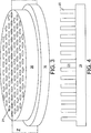
Die erste beispielhafte Struktur weist einen Stapel aus einem leitfähigen Trägermaterial
Der Durchmesser jeder Nanopore
Das AAO-Trägermaterial
Bezogen auf
Durch das extrem hohe Aspektverhältnis der Nanoporen
Bei der Atomlagenabscheidung wird durch Einleiten eines ersten Reaktanten in eine Abscheidungskammer eine Monolage eines ersten Materials in einer selbst begrenzenden Reaktion abgeschieden, bei der es mit der Bildung der Monolage aus dem ersten Material zur Sättigung kommt. Nach dem Entfernen des ersten Reaktanten wird durch Einleiten eines zweiten Reaktanten in die Abscheidungskammer eine Monolage aus einem zweiten Material in einer weiteren selbst begrenzenden Reaktion abgeschieden, bei der es mit der Bildung der Monolage aus dem zweiten Material zur Sättigung kommt. Der erste Reaktant und der zweite Reaktant werden abwechselnd in dieselbe Abscheidungskammer eingeleitet, mit einem Abpumpintervall nach jedem Durchgang zur Abscheidung einer Monolage. Im Fall eines pseudokapazitiven Materials in Form eines Metalloxids wird durch Einleiten eines metallhaltigen Reaktanten in eine Abscheidungskammer ein Metallausgangsstoff in einer selbst begrenzenden Reaktion abgeschieden, bei der es mit der Bildung der Monolage aus Metallatomen zur Sättigung kommt. Nach dem Entfernen des metallhaltigen Reaktanten wird durch Einleiten von Sauerstoffgas in die Abscheidungskammer eine Monolage Sauerstoff in einer selbst begrenzenden Reaktion abgeschieden, bei der es mit der Bildung der Monolage aus Sauerstoffatomen zur Sättigung kommt. Der Sauerstoff wird dann aus der Abscheidungskammer abgepumpt. Die Schritte Einleiten des metallhaltigen Reaktanten, Abpumpen des metallhaltigen Reaktanten, Einleiten von Sauerstoffgas und Abpumpen von Sauerstoffgas werden wiederholt ausgeführt, um eine Metalloxidschicht abzuscheiden, die die Eigenschaften der Pseudokapazität aufweist, d. h. eine ”pseudokapazitive” Metalloxidschicht. Die pseudokapazitive Materialschicht
Die Stärke der pseudokapazitiven Materialschicht
Im Allgemeinen ist die Atomlagenabscheidung notwendig, um die erforderliche hohe Konformität und die Steuerung der Geometrie insgesamt zu erreichen, damit eine zusammenhängende pseudokapazitive Materialschicht
Bei der chemischen Gasphasenabscheidung (CVD) handelt es sich um eine Gruppe von Gasphasenprozessen, bei denen es auf einer erhitzten Oberfläche zur Zerlegung des Ausgangsstoffs kommt. Auch wenn das Verfahren der chemischen Gasphasenabscheidung prinzipiell funktionieren könnte, steht bei der chemischen Gasphasenabscheidung nicht die äußerst feine Stärkensteuerung zu Verfügung, die die Atomlagenabscheidung bietet. Es steht derzeit kein chemischer Gasphasenabscheidungsprozess zur Verfügung, mit dem in Anbetracht des geringen Durchmessers der Nanoporen
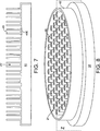
Bezogen auf
Unter Bezug auf
Die Abtragung des AAO-Trägermaterials
Durch die Abtragung des AAO-Trägermaterials
Durch die Abtragung des AAO-Trägermaterials
Die Elektrode kann somit eine Vielzahl der pseudokapazitiven Nanozylinder
Jeder pseudokapazitive Nanozylinder
Die Vielzahl der pseudokapazitiven Nanozylinder
Optional können funktionelle Molekülgruppen auf die äußeren Seitenwände und/oder inneren Seitenwände der Vielzahl der pseudokapazitiven Nanozylinder
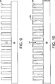
Bezogen auf
Bezogen auf
Unter Bezug auf
Die untersten Abschnitte des AAO-Trägermaterials
Unter Bezug auf
Unter Bezug auf
Die verbleibenden Abschnitte der pseudokapazitiven Materialschicht
Jeder pseudokapazitive Nanozylinder
Die zweite beispielhafte Struktur kann als Elektrode einer Energiespeichereinheit verwendet werden. Bei einer Ausführungsform weist die Elektrode eine Vielzahl der pseudokapazitiven Nanozylinder
Bezogen auf
Bezogen auf
Wenn die pseudokapazitiven Nanozylinder
Die Vielzahl der pseudokapazitiven Nanozylinder
Jeder pseudokapazitive Nanozylinder
Die dritte beispielhafte Struktur kann als Elektrode einer Energiespeichereinheit verwendet werden. In diesem Fall handelt es sich bei der Elektrode um eine ”Elektrode mit regellos angeordneten Nanozylindern”, in der die pseudokapazitiven Nanozylinder
Unter Bezug auf
Die zuvor beschriebenen spezifischen Strukturen und Prozesse können verwendet werden, um eine Ultrakondensatorelektrode bereitzustellen, mit der die derzeit erreichbare Energiedichte verdoppelt oder verdreifacht werden könnte und mit der die Blei-Säure-Batterietechnologie in zahlreichen Anwendungen wie Kraftfahrzeugbatterien und Zusatzbatterien in der Telekommunikation ersetzt werden könnte. Die offenbarten Elektroden, bei denen pseudokapazitive Nanozylinder verwendet werden, können eine ähnliche Energiedichte erreichen wie eine typische Batterie, ermöglichen jedoch 100 bis 1000 Mal mehr Lade-Entlade-Zyklen.The specific structures and processes described above can be used to provide an ultracapacitor electrode that could double or triple the currently achievable energy density and could replace lead-acid battery technology in numerous applications, such as automotive batteries and auxiliary batteries in telecommunications. The disclosed electrodes using pseudo-capacitive nanocylinders can achieve a similar energy density as a typical battery, but allow 100 to 1000 times more charge-discharge cycles.
Die Offenbarung ist zwar bezogen auf konkrete Ausführungsformen beschrieben worden, jedoch ist aus der vorhergehenden Beschreibung erkennbar, dass für den Fachmann zahlreiche Alternativen, Abwandlungen und Varianten ersichtlich sind. Die Offenbarung soll folglich alle diese Alternativen, Abwandlungen und Varianten umfassen, die in den Geltungsbereich und Geist der Offenbarung und der folgenden Ansprüche fallen.While the disclosure has been described with reference to specific embodiments, it will be apparent from the foregoing description that numerous alternatives, modifications and variations will be apparent to those skilled in the art. The disclosure is therefore intended to cover all such alternatives, modifications and variations that fall within the scope and spirit of the disclosure and the following claims.
ZITATE ENTHALTEN IN DER BESCHREIBUNG QUOTES INCLUDE IN THE DESCRIPTION
Diese Liste der vom Anmelder aufgeführten Dokumente wurde automatisiert erzeugt und ist ausschließlich zur besseren Information des Lesers aufgenommen. Die Liste ist nicht Bestandteil der deutschen Patent- bzw. Gebrauchsmusteranmeldung. Das DPMA übernimmt keinerlei Haftung für etwaige Fehler oder Auslassungen.This list of the documents listed by the applicant has been generated automatically and is included solely for the better information of the reader. The list is not part of the German patent or utility model application. The DPMA assumes no liability for any errors or omissions.
Zitierte PatentliteraturCited patent literature
- US 7084002 [0006, 0006] US 7084002 [0006, 0006]
- US 7713660 [0006] US 7713660 [0006]
Zitierte Nicht-PatentliteraturCited non-patent literature
- J. Chmiola, G. Yushin, Y. Gogotsi, C. Portet, P. Simon und P. L. Taberna, ”Anomalous increase in carbon capacitance at pore sizes less than 1 nanometer”, Science 313, 1760 (2006) [0041] J. Chmiola, G. Yushin, Y. Gogotsi, C. Portet, P. Simon and PL Taberna, "Anomalous increase in carbon capacitance at pore sizes less than 1 nanometer", Science 313, 1760 (2006) [0041]
- Stewart, M. P.; Maya, F.; Kosynkin, D. V.; Dirk, S. M.; Stapleton, J. J.; McGuiness, C. L.; Allara, D. L; Tour, J. M. ”Direct Covalent Grafting of Conjugated Molecules onto Si, GaAs, and Pd Surfaces from Aryldiazonium Salts,” J. Am. Chem Soc. 2004, 126, 370–378 [0052] Stewart, MP; Maya, F .; Kosynkin, DV; Dirk, SM; Stapleton, JJ; McGuiness, CL; Allara, D.L .; Tour, JM "Direct Covalent Grafting of Conjugated Molecules onto Si, GaAs, and Pd Surfaces from Aryldiazonium Salts," J. Am. Chem Soc. 2004, 126, 370-378 [0052]
Claims (25)
Applications Claiming Priority (3)
| Application Number | Priority Date | Filing Date | Title |
|---|---|---|---|
| US12/876,441 US8599533B2 (en) | 2010-09-07 | 2010-09-07 | Nanostructure electrode for pseudocapacitive energy storage |
| US12/876,441 | 2010-09-07 | ||
| PCT/US2011/044643 WO2012033570A1 (en) | 2010-09-07 | 2011-07-20 | Nanostructure electrode for pseudocapacitive energy storage |
Publications (1)
| Publication Number | Publication Date |
|---|---|
| DE112011102970T5 true DE112011102970T5 (en) | 2013-08-08 |
Family
ID=45770566
Family Applications (1)
| Application Number | Title | Priority Date | Filing Date |
|---|---|---|---|
| DE112011102970T Pending DE112011102970T5 (en) | 2010-09-07 | 2011-07-20 | Nanostructured electrode for pseudo-capacitive energy storage |
Country Status (8)
| Country | Link |
|---|---|
| US (1) | US8599533B2 (en) |
| JP (1) | JP5629381B2 (en) |
| CN (1) | CN103098160B (en) |
| DE (1) | DE112011102970T5 (en) |
| GB (1) | GB2497040B (en) |
| RU (1) | RU2521083C2 (en) |
| TW (1) | TWI497547B (en) |
| WO (1) | WO2012033570A1 (en) |
Families Citing this family (14)
| Publication number | Priority date | Publication date | Assignee | Title |
|---|---|---|---|---|
| US8797715B2 (en) * | 2011-03-23 | 2014-08-05 | Empire Technology Development Llc | Capacitor with parallel nanotubes |
| WO2013048465A1 (en) | 2011-09-30 | 2013-04-04 | Intel Corporation | Method of increasing an energy density and an achievable power output of an energy storage device |
| US9396883B2 (en) * | 2013-04-26 | 2016-07-19 | Intel Corporation | Faradaic energy storage device structures and associated techniques and configurations |
| CA2851434A1 (en) | 2013-05-03 | 2014-11-03 | The Governors Of The University Of Alberta | Carbon nanosheets |
| US10090376B2 (en) * | 2013-10-29 | 2018-10-02 | Micron Technology, Inc. | Methods of forming semiconductor device structures, and methods of forming capacitor structures |
| US9805880B2 (en) | 2014-01-23 | 2017-10-31 | Masdar Institute Of Science And Technology | Fabrication of enhanced supercapacitors using atomic layer deposition of metal oxide on nanostructures |
| CN106252071B (en) * | 2016-08-05 | 2018-04-03 | 南京理工大学 | A kind of height ratio capacity nanometer dielectric capacitor and preparation method thereof |
| CN106449158B (en) * | 2016-09-12 | 2018-07-17 | 武汉理工大学 | Nickel manganese composite oxide nanometer water chestnut column array electrode and preparation method thereof in titanium substrate |
| JP2017130669A (en) * | 2017-02-27 | 2017-07-27 | インテル コーポレイション | Method of increasing energy density and achievable power output of energy storage device |
| RU2678055C2 (en) * | 2017-07-14 | 2019-01-22 | ООО "Нелан-оксид плюс" | Elastic alumina nano-membrane obtaining method |
| CN108133838B (en) * | 2017-12-21 | 2019-09-17 | 北京理工大学 | A method of fake capacitance electrode is prepared based on femtosecond laser composite anode oxide |
| EP3570307A1 (en) * | 2018-05-18 | 2019-11-20 | Murata Manufacturing Co., Ltd. | Integrated energy storage component |
| RU2716700C1 (en) * | 2019-08-28 | 2020-03-16 | Акционерное общество "Концерн "Созвездие" | Method of modifying the foil surface for electrolytic capacitors |
| CN114744211B (en) * | 2022-05-13 | 2024-03-29 | 南京邮电大学 | Hyperbranched oxidized porous metal negative electrode current collector and preparation method thereof |
Citations (2)
| Publication number | Priority date | Publication date | Assignee | Title |
|---|---|---|---|---|
| US7084002B2 (en) | 2003-12-30 | 2006-08-01 | Hyundai Motor Company | Method for manufacturing a nano-structured electrode of metal oxide |
| US7713660B2 (en) | 2005-10-27 | 2010-05-11 | Korea Basic Science Institute | Method for manufacturing manganese oxide nanotube or nanorod by anodic aluminum oxide template |
Family Cites Families (23)
| Publication number | Priority date | Publication date | Assignee | Title |
|---|---|---|---|---|
| US2800616A (en) | 1954-04-14 | 1957-07-23 | Gen Electric | Low voltage electrolytic capacitor |
| US3652902A (en) * | 1969-06-30 | 1972-03-28 | Ibm | Electrochemical double layer capacitor |
| RU2123738C1 (en) * | 1997-03-21 | 1998-12-20 | Воронежский государственный технический университет | Porous coating for modifying electrolytic capacitor foil surface |
| WO1998048456A1 (en) | 1997-04-24 | 1998-10-29 | Massachusetts Institute Of Technology | Nanowire arrays |
| US6205016B1 (en) | 1997-06-04 | 2001-03-20 | Hyperion Catalysis International, Inc. | Fibril composite electrode for electrochemical capacitors |
| US6129901A (en) | 1997-11-18 | 2000-10-10 | Martin Moskovits | Controlled synthesis and metal-filling of aligned carbon nanotubes |
| KR100403611B1 (en) * | 2000-06-07 | 2003-11-01 | 삼성전자주식회사 | Metal-insulator-metal capacitor and manufacturing method thereof |
| WO2002021617A1 (en) | 2000-09-06 | 2002-03-14 | Hitachi Maxell, Ltd. | Electrode material for electrochemical element and method for production thereof, and electrochemical element |
| US7056455B2 (en) * | 2001-04-06 | 2006-06-06 | Carnegie Mellon University | Process for the preparation of nanostructured materials |
| US7355216B2 (en) * | 2002-12-09 | 2008-04-08 | The Regents Of The University Of California | Fluidic nanotubes and devices |
| CA2478004A1 (en) * | 2003-08-18 | 2005-02-18 | Wilson Greatbatch Technologies, Inc. | Use of pad printing in the manufacture of capacitors |
| US7400490B2 (en) * | 2005-01-25 | 2008-07-15 | Naturalnano Research, Inc. | Ultracapacitors comprised of mineral microtubules |
| KR100647333B1 (en) | 2005-08-31 | 2006-11-23 | 삼성전자주식회사 | Nonvolatile memory device and manufacturing method for the same |
| WO2007034873A1 (en) * | 2005-09-22 | 2007-03-29 | Honda Motor Co., Ltd. | Polarizable electrode and electrical double layer capacitor |
| RU2308112C1 (en) * | 2005-12-26 | 2007-10-10 | Общество с ограниченной ответственностью "Восток" | Multilayer anode film |
| GB0607957D0 (en) | 2006-04-21 | 2006-05-31 | Imp Innovations Ltd | Energy storage device |
| US7623340B1 (en) | 2006-08-07 | 2009-11-24 | Nanotek Instruments, Inc. | Nano-scaled graphene plate nanocomposites for supercapacitor electrodes |
| JP2008192695A (en) * | 2007-02-01 | 2008-08-21 | Matsushita Electric Ind Co Ltd | Electrode body, manufacturing method thereof and electric double-layer capacitor |
| US8085522B2 (en) * | 2007-06-26 | 2011-12-27 | Headway Technologies, Inc. | Capacitor and method of manufacturing the same and capacitor unit |
| US8535830B2 (en) * | 2007-12-19 | 2013-09-17 | The University Of Maryland, College Park | High-powered electrochemical energy storage devices and methods for their fabrication |
| US8389157B2 (en) * | 2008-02-22 | 2013-03-05 | Alliance For Sustainable Energy, Llc | Oriented nanotube electrodes for lithium ion batteries and supercapacitors |
| US7995952B2 (en) * | 2008-03-05 | 2011-08-09 | Xerox Corporation | High performance materials and processes for manufacture of nanostructures for use in electron emitter ion and direct charging devices |
| CN101625930B (en) * | 2009-06-19 | 2012-04-11 | 东南大学 | Ordered nano-tube array structure electrode material, preparation method and stored energy application |
-
2010
- 2010-09-07 US US12/876,441 patent/US8599533B2/en active Active
-
2011
- 2011-07-20 JP JP2013527076A patent/JP5629381B2/en not_active Expired - Fee Related
- 2011-07-20 GB GB1304363.3A patent/GB2497040B/en not_active Expired - Fee Related
- 2011-07-20 DE DE112011102970T patent/DE112011102970T5/en active Pending
- 2011-07-20 WO PCT/US2011/044643 patent/WO2012033570A1/en active Application Filing
- 2011-07-20 RU RU2012106418/07A patent/RU2521083C2/en not_active IP Right Cessation
- 2011-07-20 CN CN201180042946.9A patent/CN103098160B/en not_active Expired - Fee Related
- 2011-09-07 TW TW100132203A patent/TWI497547B/en not_active IP Right Cessation
Patent Citations (2)
| Publication number | Priority date | Publication date | Assignee | Title |
|---|---|---|---|---|
| US7084002B2 (en) | 2003-12-30 | 2006-08-01 | Hyundai Motor Company | Method for manufacturing a nano-structured electrode of metal oxide |
| US7713660B2 (en) | 2005-10-27 | 2010-05-11 | Korea Basic Science Institute | Method for manufacturing manganese oxide nanotube or nanorod by anodic aluminum oxide template |
Non-Patent Citations (2)
| Title |
|---|
| J. Chmiola, G. Yushin, Y. Gogotsi, C. Portet, P. Simon und P. L. Taberna, "Anomalous increase in carbon capacitance at pore sizes less than 1 nanometer", Science 313, 1760 (2006) |
| Stewart, M. P.; Maya, F.; Kosynkin, D. V.; Dirk, S. M.; Stapleton, J. J.; McGuiness, C. L.; Allara, D. L; Tour, J. M. "Direct Covalent Grafting of Conjugated Molecules onto Si, GaAs, and Pd Surfaces from Aryldiazonium Salts," J. Am. Chem Soc. 2004, 126, 370-378 |
Also Published As
| Publication number | Publication date |
|---|---|
| TW201243888A (en) | 2012-11-01 |
| JP5629381B2 (en) | 2014-11-19 |
| WO2012033570A1 (en) | 2012-03-15 |
| JP2013541836A (en) | 2013-11-14 |
| RU2521083C2 (en) | 2014-06-27 |
| GB2497040B (en) | 2014-06-18 |
| RU2012106418A (en) | 2013-10-27 |
| TWI497547B (en) | 2015-08-21 |
| CN103098160B (en) | 2016-12-07 |
| US20120057273A1 (en) | 2012-03-08 |
| CN103098160A (en) | 2013-05-08 |
| US8599533B2 (en) | 2013-12-03 |
| GB2497040A (en) | 2013-05-29 |
| GB201304363D0 (en) | 2013-04-24 |
Similar Documents
| Publication | Publication Date | Title |
|---|---|---|
| DE112011102970T5 (en) | Nanostructured electrode for pseudo-capacitive energy storage | |
| JP7142649B2 (en) | Porous solid material and manufacturing method | |
| KR102227276B1 (en) | Metal-oxide anchored graphene and carbon-nanotube hybrid foam | |
| DE102012208636B4 (en) | Process for the production of graphitic carbon particles | |
| CN102187413B (en) | Hierarchical nanowire composites for electrochemical energy storage | |
| DE112010002700B4 (en) | METHOD FOR MANUFACTURING NANOSTRUCTURED FLEXIBLE ELECTRODES AND ENERGY STORAGE DEVICES USING THESE | |
| US9653219B2 (en) | Mesoporous nanocrystalline film architecture for capacitive storage devices | |
| KR101031019B1 (en) | Method for manufacturing metal electrode having transition metallic coating layer and metal electrode manufactured thereby | |
| EP3593371B1 (en) | Deposited carbon film on etched silicon for on-chip supercapacitor | |
| US20130115453A1 (en) | Hybrid nanostructure, a method for forming the hybrid nanostructure, and an electrode including a plurality of the hybrid nanostructures | |
| DE102015120879A1 (en) | Process for producing a silicon-based porous electrode for a battery, in particular a lithium-ion battery | |
| Klankowski et al. | Higher-power supercapacitor electrodes based on mesoporous manganese oxide coating on vertically aligned carbon nanofibers | |
| Kang et al. | Ultrathin nickel hydroxide on carbon coated 3D-porous copper structures for high performance supercapacitors | |
| US20090108252A1 (en) | Lateral two-terminal nanotube devices and method for their formation | |
| US10269504B2 (en) | Supercapacitor having holes formed in carbonaceous electrodes for increasing the frequency of operation | |
| EP3298617B1 (en) | Supercapacitors with aligned carbon nanotube and method for the production thereof | |
| Xie et al. | High capacitance properties of electrodeposited PANI-Ag nanocable arrays | |
| Zhang et al. | Enlarged capacitance of TiO 2 nanotube array electrodes treated by water soaking | |
| DE19948742C1 (en) | Electrochemical capacitor used e.g. in telecommunications consists of single cell(s) with electrodes formed of an electrically conducting or semiconducting nano-structured film | |
| KR100806678B1 (en) | The fabrication method of carbon nanotube?metal oxide nanocomposite electrode | |
| DE10053276C1 (en) | Electrochemical capacitor used as double-layer capacitor or super-capacitor comprises single cell(s) having electrode made from nano-structured film, counter electrode, and thin film electrolyte covering electrode | |
| DE102005032513B4 (en) | Layer electrode for electrochemical double-layer capacitors, manufacturing method and electrochemical double-layer capacitor | |
| KR101579177B1 (en) | Composite electrode for supercapacitor and preparation method thereof | |
| DE102012215889A1 (en) | energy storage | |
| WO2022167111A1 (en) | Method for producing high-current capacitors by laser technology |
Legal Events
| Date | Code | Title | Description |
|---|---|---|---|
| R012 | Request for examination validly filed | ||
| R079 | Amendment of ipc main class |
Free format text: PREVIOUS MAIN CLASS: H01G0009058000 Ipc: H01G0011220000 |
|
| R079 | Amendment of ipc main class |
Free format text: PREVIOUS MAIN CLASS: H01G0009058000 Ipc: H01G0011240000 Effective date: 20140224 Free format text: PREVIOUS MAIN CLASS: H01G0011220000 Ipc: H01G0011240000 Effective date: 20140224 Free format text: PREVIOUS MAIN CLASS: H01G0009058000 Ipc: H01G0011220000 Effective date: 20140224 |
|
| R081 | Change of applicant/patentee |
Owner name: GLOBALFOUNDRIES U.S. INC., SANTA CLARA, US Free format text: FORMER OWNER: INTERNATIONAL BUSINESS MACHINES CORPORATION, ARMONK, N.Y., US Owner name: GLOBALFOUNDRIES INC., KY Free format text: FORMER OWNER: INTERNATIONAL BUSINESS MACHINES CORPORATION, ARMONK, N.Y., US |
|
| R082 | Change of representative |
Representative=s name: RICHARDT PATENTANWAELTE PARTG MBB, DE |
|
| R081 | Change of applicant/patentee |
Owner name: GLOBALFOUNDRIES U.S. INC., SANTA CLARA, US Free format text: FORMER OWNER: GLOBALFOUNDRIES US 2 LLC (N.D.GES.DES STAATES DELAWARE), HOPEWELL JUNCTION, N.Y., US Owner name: GLOBALFOUNDRIES INC., KY Free format text: FORMER OWNER: GLOBALFOUNDRIES US 2 LLC (N.D.GES.DES STAATES DELAWARE), HOPEWELL JUNCTION, N.Y., US |
|
| R082 | Change of representative |
Representative=s name: RICHARDT PATENTANWAELTE PARTG MBB, DE |
|
| R016 | Response to examination communication | ||
| R081 | Change of applicant/patentee |
Owner name: GLOBALFOUNDRIES U.S. INC., SANTA CLARA, US Free format text: FORMER OWNER: GLOBALFOUNDRIES INC., GRAND CAYMAN, KY |
|
| R082 | Change of representative |
Representative=s name: RICHARDT PATENTANWAELTE PARTG MBB, DE |
|
| R082 | Change of representative |
Representative=s name: GRUENECKER PATENT- UND RECHTSANWAELTE PARTG MB, DE |
|
| R016 | Response to examination communication | ||
| R016 | Response to examination communication |