CN111404220A - Battery management chip, battery management system, electronic equipment and power supply method - Google Patents
Battery management chip, battery management system, electronic equipment and power supply method Download PDFInfo
- Publication number
- CN111404220A CN111404220A CN202010192571.5A CN202010192571A CN111404220A CN 111404220 A CN111404220 A CN 111404220A CN 202010192571 A CN202010192571 A CN 202010192571A CN 111404220 A CN111404220 A CN 111404220A
- Authority
- CN
- China
- Prior art keywords
- voltage
- battery
- battery management
- converter
- output
- Prior art date
- Legal status (The legal status is an assumption and is not a legal conclusion. Google has not performed a legal analysis and makes no representation as to the accuracy of the status listed.)
- Pending
Links
Images


Classifications
-
- H—ELECTRICITY
- H02—GENERATION; CONVERSION OR DISTRIBUTION OF ELECTRIC POWER
- H02J—CIRCUIT ARRANGEMENTS OR SYSTEMS FOR SUPPLYING OR DISTRIBUTING ELECTRIC POWER; SYSTEMS FOR STORING ELECTRIC ENERGY
- H02J7/00—Circuit arrangements for charging or depolarising batteries or for supplying loads from batteries
- H02J7/0013—Circuit arrangements for charging or depolarising batteries or for supplying loads from batteries acting upon several batteries simultaneously or sequentially
-
- H—ELECTRICITY
- H02—GENERATION; CONVERSION OR DISTRIBUTION OF ELECTRIC POWER
- H02J—CIRCUIT ARRANGEMENTS OR SYSTEMS FOR SUPPLYING OR DISTRIBUTING ELECTRIC POWER; SYSTEMS FOR STORING ELECTRIC ENERGY
- H02J7/00—Circuit arrangements for charging or depolarising batteries or for supplying loads from batteries
- H02J7/0063—Circuit arrangements for charging or depolarising batteries or for supplying loads from batteries with circuits adapted for supplying loads from the battery
Abstract
The present disclosure provides a battery management chip, including: the voltage conversion part comprises a voltage reduction type DC-DC switch converter, the input end of the voltage conversion part is connected with the output voltage of the battery, and the voltage reduction type DC-DC switch converter converts the output voltage of the battery into the output voltage of the voltage conversion part and outputs the output voltage through the output end of the voltage conversion part; and the battery management part detects and/or controls the battery, and the power supply end of the battery management part is connected with the output end of the voltage conversion part so as to output voltage through the voltage conversion part to supply power to the battery management part. The disclosure also provides a battery management system, electronic equipment and a power supply method.
Description
Technical Field
The present disclosure relates to the field of battery management technologies, and in particular, to a battery management chip and a battery management system. Electronic equipment and power supply method.
Background
The BMS System (Battery Management System) refers to a System that manages and controls a Battery. The battery to be managed and controlled may include a lithium battery, and may also include other types of batteries. The main functions of the BMS system include: the state of the battery is monitored in real time, and management and control of the internal state of the battery are realized by detecting external characteristic parameters (such as voltage, current, temperature and the like) of the battery and adopting a proper algorithm. BMS systems are generally powered by the highest voltage of the battery or battery pack. And the modules in the BMS system need to be powered with low voltage, such as 5V, 3.3V, or 1.8V, etc. Therefore, the conventional BMS system also requires a power management system to provide it with a low-voltage power supply. That is, the BMS needs to cooperate with the power management system to work normally, which makes the whole system complicated, numerous components, bulky and costly, and these disadvantages are not good for the development trend of miniaturization and integration of products.
Furthermore, in chinese patent application publication No. CN108964162A, the battery management system uses the power management system of the DC/DC converter to supply power, and in addition to the above disadvantages, the control chip of the DC/DC power unit in the DC/DC converter is directly powered by the battery, that is, the control chip uses high-voltage power as the working power source, so the control chip must be a high-voltage-resistant chip. In this patent application, in addition to supplying power through an external management power supply system, a high-voltage chip is also required, which causes problems such as high power consumption.
In the case of a lithium battery, the safe operation area of the battery is determined by the current, temperature, voltage, and the like of the battery. If the voltage threshold value is exceeded, the battery is overcharged, the battery can be rapidly damaged and explode when the voltage threshold value is exceeded, and the battery can be damaged when the voltage threshold value is continuously discharged. The lithium battery discharges outside a certain temperature range to damage the service life of the battery, the lithium battery which works outside the allowable temperature range for a long time is easy to generate thermal runaway and spontaneous combustion, and even if the thermal runaway is not generated, the organic electrolyte can support combustion. The life of the lithium ion battery may be impaired by large current discharge or rapid charge. These limits also vary depending on the chemical composition of the cell itself. The BMS system is used to ensure that the cells within the managed battery are operated within their safe operating areas. Particularly, a large-scale battery pack composed of a large number of unit cells connected in series is more likely to cause overcharge or overdischarge due to voltage imbalance of the internal unit cells.
Disclosure of Invention
To solve at least one of the above technical problems and others, the present disclosure provides a battery management chip, a battery management system, an electronic device, and a power supply method.
According to one aspect of the present disclosure, a battery management chip includes:
a voltage conversion part including a step-down DC-DC switching converter, an input end of the voltage conversion part being connected to a battery output voltage, the step-down DC-DC switching converter converting the battery output voltage into a voltage conversion part output voltage and outputting the voltage conversion part output voltage through an output end of the voltage conversion part; and
the battery management part detects and/or controls the battery, and the power supply end of the battery management part is connected with the output end of the voltage conversion part so as to supply power to the battery management part through the voltage output by the voltage conversion part.
According to at least one embodiment of the present disclosure, the battery management part includes an interface circuit, the interface circuit communicates with an MCU external to the battery management chip, and the battery management part transmits and receives information to and from the external control through the interface circuit, so that the battery management part performs detection and/or management control on the battery,
and the power supply end of the MCU is connected with the output end of the voltage conversion part so as to supply power to the MCU through the voltage output by the voltage conversion part.
According to at least one embodiment of the present disclosure, the battery management part includes a signal processing unit for processing a detection signal of the battery and/or a management control signal of the battery.
According to at least one embodiment of the present disclosure, the battery management part includes a detection voltage input terminal that receives a voltage of each battery in a battery pack formed by N batteries connected in series, where N is an integer greater than 2.
According to at least one embodiment of the present disclosure, the battery management section includes a selection circuit that selects a battery voltage of one battery in the battery pack at one time or selects respective battery voltages of M batteries in the battery pack at one time, thereby obtaining the battery voltage selected by the selection circuit, where 2 ≦ M ≦ N.
According to at least one embodiment of the present disclosure, the battery management part includes a first analog-to-digital converter,
in a case where the selection circuit selects the voltage of one battery in the battery pack at a time, the number of the first analog-to-digital converters is one, so that the battery voltage of the selected one battery is converted into a digital signal by one of the first analog-to-digital converters and supplied to the signal processing unit, and
in a case where the selection circuit selects the respective cell voltages of the M cells in the battery pack at one time, the number of the first analog-to-digital converters is M, so that the respective cell voltages of the selected M cells are converted into digital signals by the M first analog-to-digital converters, respectively, and supplied to the signal processing unit.
According to at least one embodiment of the present disclosure, the battery management part includes a detection current input terminal that receives current information when the battery is charged or discharged.
According to at least one embodiment of the present disclosure, the battery management part includes a second analog-to-digital converter that converts the current information into a digital signal and supplies the digital signal to the signal processing unit.
According to at least one embodiment of the present disclosure, the battery management part includes a battery temperature acquisition unit, by which a temperature value of the battery is obtained and provided to the signal processing unit.
According to at least one embodiment of the present disclosure, the battery management part includes a charge driving unit and a discharge driving unit, and the signal processing unit controls the charge driving unit and the discharge driving unit according to a detection signal of a battery and/or a control signal from an MCU so as to stop or start charging or discharging of the battery.
According to at least one embodiment of the present disclosure, the voltage conversion section further comprises an L DO voltage converter, the L DO voltage converter converting the battery output voltage into a voltage conversion section output voltage,
wherein the voltage converting part is controlled to convert the battery output voltage into the voltage converting part output voltage through the step-down type DC-DC switching converter, or to convert the battery output voltage into the voltage converting part output voltage through the L DO voltage converter, or to convert the battery output voltage into the voltage converting part output voltage through the step-down type DC-DC switching converter and the L DO voltage converter.
According to at least one embodiment of the present disclosure, the L DO voltage converter includes an amplifier-based L DO voltage converter and a comparator-based L DO voltage converter, the L DO voltage converter may be switched to an amplifier-based L DO voltage converter or a comparator-based L DO voltage converter to convert the battery output voltage to a voltage conversion section output voltage.
According to at least one embodiment of the present disclosure, the voltage converting part supplies the output voltage through L DO voltage converter or through a series connection of a buck-type DC-DC switching converter and L DO voltage converter when the battery management chip is in a state of collecting battery information, and supplies the output voltage through the buck-type DC-DC switching converter when the battery management chip is not in a state of collecting battery information.
According to at least one embodiment of the present disclosure, the voltage conversion part is controlled by a signal processing unit inside the battery management chip and/or an MCU outside the battery management chip to provide the output voltage through L DO voltage converter, or through a series connection of a buck DC-DC switching converter and a L DO voltage converter, or through a buck DC-DC switching converter.
According to another aspect of the present disclosure, a battery management system includes: a battery management chip as described above; and the MCU is communicated with the battery management chip through an interface circuit of the battery management part and is powered by the output voltage of the voltage conversion part.
According to at least one embodiment of the present disclosure, the battery management chip further includes a charge control switch and a discharge control switch for controlling charge and discharge of the battery by control signals from a charge driving unit and a discharge driving unit of the battery management chip.
According to yet another aspect of the disclosure, an electronic device includes: a battery or battery pack that powers other components of the electronic device; and a battery management system as described above for controlling the charging or discharging of the battery or battery pack.
According to yet another aspect of the present disclosure, a method of powering a battery management system through a battery management chip includes: receiving a battery output voltage of a battery or a battery pack; carrying out voltage reduction processing on the output voltage of the battery through a voltage reduction type DC-DC switch converter inside the battery management chip; and supplying the voltage after voltage reduction processing to a battery management part as a power supply voltage of the battery management part, wherein the battery management part is integrated in the battery management chip and is used for detecting and/or controlling the battery or the battery pack.
According to at least one embodiment of the present disclosure, the voltage after the voltage reduction processing is further provided to an MCU external to the battery management chip, wherein the MCU and the battery management part communicate with each other to perform detection and/or management control on the battery.
According to at least one embodiment of the present disclosure, the battery output voltage is down-converted by cooperation of a down-type DC-DC switching converter and an L DO voltage converter, wherein the down-type DC-DC switching converter and a L DO voltage converter are controlled to convert the battery output voltage into a down-converted voltage through the down-type DC-DC switching converter, or convert the battery output voltage into a down-converted voltage through a L DO voltage converter, or convert the battery output voltage into a down-converted voltage through the down-type DC-DC switching converter and a L DO voltage converter.
According to at least one embodiment of the present disclosure, the L DO voltage converter includes an amplifier-based L DO voltage converter and a comparator-based L DO voltage converter, the L DO voltage converter may be switched to an amplifier-based L DO voltage converter or a comparator-based L DO voltage converter to convert the battery output voltage to a voltage conversion section output voltage.
Drawings
The accompanying drawings, which are included to provide a further understanding of the disclosure and are incorporated in and constitute a part of this specification, illustrate exemplary embodiments of the disclosure and together with the description serve to explain the principles of the disclosure.
Fig. 1 is a schematic diagram of a battery management system according to one embodiment of the present disclosure.
Fig. 2 is a schematic diagram of a battery management chip according to one embodiment of the present disclosure.
Fig. 3 is a schematic diagram of a battery management chip according to one embodiment of the present disclosure.
Fig. 4 is a schematic diagram of a voltage conversion part according to an embodiment of the present disclosure.
Fig. 5 is a schematic diagram of a battery management chip according to one embodiment of the present disclosure.
Fig. 6 is a schematic diagram of a voltage conversion section according to an embodiment of the present disclosure.
Fig. 7 is a schematic diagram of a voltage conversion section according to an embodiment of the present disclosure.
Fig. 8 is a schematic diagram of a voltage conversion part according to an embodiment of the present disclosure.
Fig. 9 is a schematic diagram of a voltage conversion section according to an embodiment of the present disclosure.
Fig. 10 is a schematic diagram of a voltage conversion part according to an embodiment of the present disclosure.
Fig. 11 is a schematic diagram of a switching circuit according to one embodiment of the present disclosure.
Detailed Description
The present disclosure will be described in further detail with reference to the drawings and embodiments. It is to be understood that the specific embodiments described herein are for purposes of illustration only and are not to be construed as limitations of the present disclosure. It should be further noted that, for the convenience of description, only the portions relevant to the present disclosure are shown in the drawings.
It should be noted that the embodiments and features of the embodiments in the present disclosure may be combined with each other without conflict. Technical solutions of the present disclosure will be described in detail below with reference to the accompanying drawings in conjunction with embodiments.
Unless otherwise indicated, the illustrated exemplary embodiments/examples are to be understood as providing exemplary features of various details of some ways in which the technical concepts of the present disclosure may be practiced. Accordingly, unless otherwise indicated, features of the various embodiments may be additionally combined, separated, interchanged, and/or rearranged without departing from the technical concept of the present disclosure.
The use of cross-hatching and/or shading in the drawings is generally used to clarify the boundaries between adjacent components. As such, unless otherwise noted, the presence or absence of cross-hatching or shading does not convey or indicate any preference or requirement for a particular material, material property, size, proportion, commonality between the illustrated components and/or any other characteristic, attribute, property, etc., of a component. Further, in the drawings, the size and relative sizes of components may be exaggerated for clarity and/or descriptive purposes. While example embodiments may be practiced differently, the specific process sequence may be performed in a different order than that described. For example, two processes described consecutively may be performed substantially simultaneously or in reverse order to that described. In addition, like reference numerals denote like parts.
When an element is referred to as being "on" or "on," "connected to" or "coupled to" another element, it can be directly on, connected or coupled to the other element or intervening elements may be present. However, when an element is referred to as being "directly on," "directly connected to" or "directly coupled to" another element, there are no intervening elements present. For purposes of this disclosure, the term "connected" may refer to physically, electrically, etc., and may or may not have intermediate components.
For descriptive purposes, the present disclosure may use spatially relative terms such as "below … …," below … …, "" below … …, "" below, "" above … …, "" above, "" … …, "" higher, "and" side (e.g., as in "side wall") to describe one component's relationship to another (other) component as illustrated in the figures. Spatially relative terms are intended to encompass different orientations of the device in use, operation, and/or manufacture in addition to the orientation depicted in the figures. For example, if the device in the figures is turned over, elements described as "below" or "beneath" other elements or features would then be oriented "above" the other elements or features. Thus, the exemplary term "below … …" can encompass both an orientation of "above" and "below". Further, the devices may be otherwise positioned (e.g., rotated 90 degrees or at other orientations) and the spatially relative descriptors used herein interpreted accordingly.
According to one embodiment of the present disclosure, a battery management chip and a battery management system are provided.
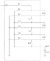
Fig. 1 illustrates a battery management system including a battery management chip according to an embodiment of the present disclosure. The following description will be given by taking a lithium battery as an example, but it will be understood by those skilled in the art that the battery may be a single battery, or may be a battery of other types of batteries. For example, as shown in fig. 1, the battery pack is formed by connecting a plurality of batteries in series, such as BAT1, BAT2.
As shown in fig. 1, the battery management system 10 may include a battery management chip 100 and an MCU (micro control unit) 200. The battery management chip 100 can be used for data acquisition and protection of the battery.
Next, the battery management chip 100 of the present disclosure will be explained first. The battery management chip 100 may include a voltage conversion part 110 and a battery management part 120. It should be noted that the voltage conversion unit 110 and the battery management unit 120 are integrated into a chip, so that the battery management unit 120 can be powered by the voltage conversion unit 110 inside the chip, and a power management system outside the chip is not needed to provide low-voltage power.
The voltage converting part 110 may include a step-down DC-DC switching converter, and the input terminal IN of the voltage converting part 110 may be connected with an output voltage of the battery, wherein the output voltage may be a total voltage of the battery pack when the battery pack is IN a form of the battery pack, a partial voltage of the battery pack, or the like. And the output voltage of the battery can be filtered by the RC filter circuit to obtain the voltage VCC. The step-down DC-DC switching converter converts the battery output voltage into a voltage conversion part output voltage and outputs it through an output terminal of the voltage conversion part 110.
The specific form for the voltage converter 110 will be described in detail below.
The battery management part 120 may include a digital signal processing unit 121, a selection circuit 121, a first analog-to-digital converter 122, a second analog-to-digital converter 123, a battery temperature acquisition unit 124, a charge control unit 125, and a discharge control unit 126.
The battery management chip 100 may be used to detect voltage information of the battery pack. The battery management part 120 may include sensing voltage input terminals SENSE1, SENSE2, … …, SENSE that receive a voltage of each battery in a battery pack formed by N batteries connected in series, where N is an integer greater than 2.
The voltage of each battery of the battery pack may be first reduced in noise and interference by a filter circuit composed of Rf1 and Cf1, Rf2 and Cf2, … …, Rfn and Cfn, and then connected to the input terminals SENSE1, SENSE2, … …, SENSE of the battery management chip 100.
The selection circuit 121 may receive a voltage signal of each battery and perform selection. For example, the positive terminal voltage and the negative terminal voltage of one of the batteries are selected at the same time, and sent to the first analog-to-digital converter (ADC1)122 for sampling and quantization, and converted into digital signals; the voltages of the positive terminals and the negative terminals of two or more batteries can be selected at the same time, and sent to the first analog-to-digital converter (ADC1)122 for sampling and quantization, and then converted into digital signals. The converted digital signal is sent to the digital signal processing unit 121.
The battery management chip 100 may be used to detect current information of the battery pack. When the battery pack is charged or discharged, the charging current or the discharging current of the battery generates a voltage drop through the sampling resistor Rsense connected in series in the current loop, and the second analog-to-digital converter (ADC2)123 collects information of the voltage drop generated by the sampling resistor Rsense, so as to obtain the charging or discharging current information of the battery pack, and sends the current information to the digital signal processing unit 121. Thereby, based on the current information, the protection circuit is controlled, and the protection circuit may include a charging control unit 125 and a discharging control unit 126. The charge control unit 125 and the discharge control unit 126 control the charge control power device M _ CHG and the discharge control power device M _ DCH in the current loop of the battery, respectively, so as to control the charge and discharge of the battery pack when the voltage is abnormal. In addition, the current signal of the battery pack can be used for calculating the electric quantity of the battery pack, and the calculation can be realized by a coulometer.
The battery management chip 100 may be used to detect temperature information of the battery pack. The detection of the temperature may be implemented by constituting a series circuit of the constant temperature resistor Rs and the thermistor R _ ntc, wherein one end of the series circuit may be connected to the voltage output terminal of the voltage conversion part 110 and the other end may be grounded, and the detection terminal may be a connection node of the constant temperature resistor Rs and the thermistor R _ ntc. R _ ntc is placed close to the battery pack to ensure that its temperature is close to the temperature of the battery. The thermistor may be a Negative Temperature Coefficient (NTC) thermistor, i.e. the resistance of the thermistor decreases with increasing Temperature. The voltage of the connection node of Rs and R _ ntc is supplied to the battery temperature acquisition unit 124 of the battery management chip 100, and the temperature information of the battery is obtained by the acquired voltage value, the output voltage value of the voltage conversion part 110, and the characteristic (temperature coefficient) in combination with the resistance of R _ ntc. And the temperature information of the battery is transmitted to the digital signal processing unit 121. Thus, when the temperature is abnormal, the charging and discharging of the battery pack can be controlled by controlling the charging control power device M _ CHG and the discharging control power device M _ DCH.
The digital signal processing unit 121 estimates the current state of the battery, such as the capacity of the battery, the state of charge of the battery (the current electric quantity of the battery), and the like, through a model algorithm according to the obtained battery information, including information such as the voltage, the current, the temperature, and the like of the above battery pack. For example, when an abnormality occurs, the digital signal processing unit 121 may perform control, such as initialization of the system, parameter configuration, execution of a detection function, execution of a protection function, and the like, to ensure that each battery cell operates in a safe region. If the battery is in a charging state, when it is detected that the voltage of one of the battery cells exceeds the set threshold voltage for charge protection, the dsp 121 controls the charge control unit 125 to turn off the external charge control power device M _ CHG, and stops the charging function to protect the battery. The functions of this part may be completed by the digital signal processing unit 121, may also be completed by the MCU200, and may also be completed by the cooperation of the digital signal processing unit 121 and the MCU 200. In addition, the digital signal processing unit 121 may pass through the interface circuit I2C completes communication with the MCU200, and the digital signal processing unit 121 may also perform the above processing through a control signal of the MCU 200.
According to the embodiment of the present disclosure, the power supply terminal of the MCU200 is connected to the voltage output terminal of the voltage conversion part 110, and the MCU200 is directly powered by the output voltage of the voltage conversion part 110. This can effectively reduce power consumption and the requirements on the MCU200 itself.
The voltage conversion section 110 may include a Buck DC-DC switching converter, which may be a Buck power converter or a switched capacitor voltage converter, for example, the voltage conversion section 110 may include a combined Buck DC-DC switching converter and L DO voltage converter circuit, which may be a Buck power converter or a switched capacitor voltage converter, for example.
As an example, fig. 2 shows a case where the voltage conversion section 110 is a Buck power converter. Under the condition that adopts Buck power converter, the on-off control of accessible high frequency and the filtering of inductance and electric capacity, realize the function of step-down, and because Buck power converter's efficiency can reach 90% even higher usually, consequently this lithium cell group's battery management chip's power conversion efficiency will be greater than traditional lithium cell group's battery management chip far away, in addition, the battery management chip that the battery management chip of the lithium cell group of adoption Buck power converter's battery management chip that generates heat will be less than traditional framework far away, therefore this lithium cell group's battery management chip has lower temperature, longer life-span and higher reliability.
As shown in fig. 2, the input terminal of the Buck power converter may be connected to the voltage of the battery pack (as in fig. 1) as an input voltage, and the output terminal thereof outputs the voltage VOUT through the connection point of the inductor and the capacitor connected in series, and the output voltage may be used as a feedback voltage. Meanwhile, the output voltage VOUT serves as a supply voltage for a battery management section inside the chip and also as a supply voltage for an MCU outside the chip.
As an example, fig. 3 shows a case where the voltage conversion section 110 is a switched capacitor voltage converter. As shown in fig. 3, the switched capacitor voltage converter includes a control module of the switched capacitor voltage converter and m external capacitors, where m is a positive integer and is greater than or equal to 1, C1, … …, Cm-1, and Cm. The capacitance selection is controlled by the switching control in the control module of the switched capacitor voltage converter, thereby achieving voltage conversion.
When the switched capacitor voltage converter is used for voltage reduction conversion, input voltage is added to the capacitors connected in series in a certain time period, and the capacitors are connected to the output in parallel in another time period, so that voltage reduction conversion of a power supply is realized, and output current larger than the input current is provided to improve efficiency.
As shown in fig. 3, the input terminal of the control module of the switched capacitor voltage converter is connected to the voltage of the battery pack (as in fig. 1) as an input voltage, and the output voltage VOUT of the output terminal thereof may be used as a feedback voltage. Meanwhile, the output voltage VOUT serves as a supply voltage for a battery management section inside the chip and also as a supply voltage for an MCU outside the chip.
Fig. 4 shows a specific example of a switched capacitor voltage converter. In this example, the number of the capacitors of the switched capacitor voltage converter is 3, the control module of the switched capacitor voltage converter may include ten switches, one end of the first switch K1 serves as an input terminal of the control module of the switched capacitor voltage converter, the other end of the first switch K1 is connected with one end of the second switch K2 and one end of the first capacitor C1, the other end of the second switch K2 is connected with one end of the fourth switch K4, one end of the sixth switch K6 and one end of the tenth switch K10, and serves as an output terminal and a feedback terminal of the control module of the switched capacitor voltage converter.
One end of the third switch K3 is connected to one end of the fifth switch K5, one end of the tenth switch K10, and the ground, and the other end of the third switch K3 is connected to the other end of the first capacitor C1 and one end of the seventh switch K7.
The other end of the fourth switch K4 is connected to the other end of the seventh switch K7 and one end of the second capacitor C2, the other end of the fifth switch K5 is connected to one end of the eighth switch K8 and the other end of the second capacitor C2, the other end of the sixth switch K6 is connected to the other end of the eighth switch K8 and one end of the third capacitor C3, and the other end of the ninth switch K9 is connected to the other end of the tenth switch K10 and the other end of the third capacitor C3.
The switched capacitor power converter comprises capacitors C1, C2, C3 and Cout and two groups of switches (the first group of switches are K2, K3, K4, K5, K6 and K9, and the second group of switches are K1, K7, K8 and K10). When the first group of switches is turned off and the second group of switches is turned on, the input voltage is applied to the capacitors connected in series by C1, C2, C3 and Cout; when the first set of switches is closed and the second set of switches is open, C1, C2, C3 discharge to Cout. By alternately controlling the two sets of switches, the input power supply can be converted into an output voltage which is not higher than 1/4 times of the input voltage, and meanwhile, the output current is 4 times of the output current, so that the voltage conversion from the input end IN to the output end VOUT is realized.
As an example, fig. 5 shows a case where the voltage conversion section 110 includes a Buck power converter and L DO voltage converter combined circuit.
In fig. 5, VCC is a battery voltage or a filtered battery voltage (as shown in fig. 1), and in this case, the voltage converter 110 is a Buck power converter, a L DO voltage converter, or a combined circuit of the Buck power converter and a L DO voltage converter by controlling the switches S1 to S5.
For example, when S3, S5, and S2 are turned off and S1, S4 are turned on, the voltage conversion unit 110 is a Buck power converter, whereas when S3, S5, and S2 are turned on and S1, S4 are turned off, the voltage conversion unit 110 is a L DO voltage converter, and when S3, S5 are turned off and S1, S2, and S4 are turned on, the voltage conversion unit 110 is a combined circuit of a Buck power converter and a L DO voltage converter.
The Buck power converter is compared to the L DO voltage converter as follows.
The energy management system has the advantages of simple structure, small ripple, low cost, small volume, etc., but has the disadvantage of inefficiency, particularly when the battery voltage (the total voltage of the battery system) is much higher than the voltage required by the battery management system power supply, such as for a battery system with 4 lithium batteries connected in series, if the battery management system has a supply voltage of 3.3V, an L DO voltage converter is used, the voltage of 3.6 × V of 4 lithium batteries is 14.4V to 3.3V, the efficiency will not exceed 3.3V/14.4V 23%, since the voltage converter supplies power to the modules in the management chip of the battery pack and the external components, the power efficiency of the entire system does not exceed 23%, the power efficiency of the power supply is determined by the operating conditions, cannot be improved by design, the improvement of reducing the resistance on the wires, increasing the power efficiency of the power tubes, etc., approaches the efficiency of 23% and the efficiency of the external components, thus the efficiency of the power supply is not increased by the conventional thermal resistance management system, such as the efficiency of the battery management system 23V 7C 3V 23V, the efficiency of the battery management system is not increased by the conventional high thermal resistance, the thermal resistance of the thermal management system, which may cause the thermal management system to increase of the efficiency of the thermal energy management system, such as the thermal energy management system, the thermal energy management system 23C 3V 23C 3V 7C 3V 23V 7C 3V 7C 3V 23V 7C 3V 23C 7C 3V 23V 7C 3V 23C 7C 3V 23V 7C 3V 23V.
The switching type DC-DC voltage converter such as a Buck power converter is adopted as the voltage converter, the efficiency of power conversion is obviously improved, so that the efficiency of a battery management chip of a lithium battery pack is higher, the use is more flexible, the battery management chip of the lithium battery pack has lower temperature, longer service life and higher reliability, the power conversion efficiency of a battery management system using the battery management chip of the lithium battery pack is greatly improved, and the switching type DC-DC voltage converter also has lower temperature, longer service life and higher reliability.
Accessible high frequency's on-off control and inductance and electric capacity's filtering among the Buck power converter, realize the function of step-down, and because Buck power converter's efficiency can reach 90% even higher usually, consequently, the battery management chip of the lithium cell group of L DO voltage converter will be greater than far away to the power conversion efficiency of the battery management chip of this lithium cell group, in addition, the battery management chip of the lithium cell group that adopts Buck power converter's lithium cell group will be less than L DO voltage converter's lithium cell group far away to generating heat, therefore the data acquisition of this lithium cell group and protection chip have lower temperature, longer life-span and higher reliability.
Under the application condition that the input voltage is far larger than the output voltage, the voltage drop can be far smaller than the voltage drop (VIN-VOUT) of a power tube of a L DO voltage converter under the same application condition, so that the conduction loss of the power tube of the Buck power converter under the same condition is far less than that of a L DO voltage converter.
The normal operating current of the battery management chip of the lithium battery pack and the external load is 20 mA., the power loss of the battery management system containing the L DO voltage converter is (14.4V-3.3V) × 20mA is 222 mW., and the power loss of the battery management system containing the Buck power converter is 3.3V × 20mA × (1-90%)/90%/7.3 mW., so the condition of the Buck power converter is far lower than that of the L DO voltage converter.
Power dissipation in a battery management system is typically dissipated in the form of heat generated by the battery management chip of the lithium battery pack, which results in different heat generation for battery management systems using different architectures. The heat generated by the chip is dissipated to the surrounding environment through the package, and the temperature of the chip is increased. For the same package, the greater the heat generated by the chip, the higher the temperature of the chip during normal operation, and the higher the temperature of the chip, the faster the chip ages, the shorter the life, and the lower the reliability.
If the number of battery nodes is 16, the input power voltage VCC of the system is as high as 3.6V × 16-57.6V, assuming that the supply voltage of the battery management chip and the external components of the lithium battery pack is 3.3V and the operating current is 20mA, the battery management chip of the lithium battery pack of the L DO voltage converter has a maximum power efficiency of 3.3V/57.6V-5.7% and a power loss of (57.6V-3.3V) × 20 mA-1086 mW, whereas the battery management chip of the lithium battery pack containing the Buck power converter has a power efficiency of 80% (mainly the conduction loss and the switching loss of the power devices) and a power loss of 3.3V × 20 mA/80% × (1-80%) -16.5 mW., so that the Buck scheme can be improved by more than 14 times, and the power loss can be reduced to 1.5% of the conventional scheme, i.5% of DO L.
Compared with the L DO voltage converter, the Buck power converter has certain output ripple waves due to the working characteristicsWhen the load is constant and the power converter works stably, the output current and the output voltage of the L DO power converter are also constant, but when the Buck power converter works, the control module controls the high-frequency switching of the power tube, the working frequency is set to fsw, and when the Buck power converter works, one cycle 1/fsw is divided into 2 time segments, namely, the conduction time and the free-wheeling time, in the conduction time, the power tube between the switching end SW1 of the control module of the Buck power converter and the input power supply is conducted, the voltage of the switching end SW1 is close to the input voltage, in the free-wheeling time, the power tube between the switching end switch of the control module of the Buck power converter and the ground is conducted, the voltage of the switching end switch is close to the ground voltage, therefore, the voltage at two ends of the inductor is also a high-frequency variable quantity, the current of the inductor, the output voltage Vout2 of the Buck power converter is also high-frequency fluctuating, the effects of: taking a 16-cell system as an example, if L uH and Cout 10uF are used and the operating frequency is 200kHz, the ripple of the output voltage will be Δ VOUT=3.3mV。
Therefore, when the switch type DC-DC voltage converter adopts a Buck power converter, the function of voltage reduction can be realized through high-frequency switch control and filtering of an inductor and a capacitor, and the efficiency of the Buck power converter can reach 90% or even higher generally, so that the power conversion efficiency of the battery management chip of the lithium battery pack is far greater than that of the battery management chip of the lithium battery pack containing L DO, and in addition, the heat generation of the battery management chip of the lithium battery pack adopting the Buck power converter is far less than that of the battery management chip of the lithium battery pack of a traditional framework, so that the battery management chip of the lithium battery pack has lower temperature, longer service life and higher reliability.
In addition, according to different application requirements, a user can arbitrarily configure the Buck-frame voltage converter and the L DO-frame voltage converter into the Buck mode and the L DO mode, the Buck-frame voltage converter has the characteristics of high efficiency and ultralow standby power consumption when in the Buck mode, and has the advantage of low ripple when working in the L DO mode, and the innovative structure saves the circuit cost to the maximum extent through a control logic, a driving circuit and a feedback detection module which are shared by ingenious and innovative modes.
In summary, in this embodiment of the present disclosure, the Buck power converter and the L DO voltage converter of the voltage conversion section 110 may be switched according to actual situations, for example, when the input voltage is high (for example, greater than 5V) and/or the input/output voltage difference is high, the switching may be performed to only use the Buck power converter, and vice versa, the switching may be performed to only use the L DO voltage converter, when the output current is large (for example, greater than 2A), the switching may be performed to only use the Buck power converter, and vice versa, the switching may be performed to only use the L DO voltage converter, and vice versa when the system has a high requirement for output ripple and/or voltage stabilization, the switching may be performed to only use the Buck power converter, and the switching may be performed to only use the L DO voltage converter when the system has a high requirement for switching efficiency, and the switching may be performed to use the Buck + L voltage converter when the input voltage is high and/or the input/output voltage difference is high and the output current ratio is large.
It will be appreciated by those skilled in the art that although not illustrated in detail, the switched capacitor voltage converter described above may also be used with an L DO voltage converter, in which case the Buck power converter may be replaced with a switched capacitor voltage converter.
Fig. 6 and 7 show an embodiment according to the present disclosure, in which a Buck power converter or an L DO voltage converter can be selected as the voltage conversion section 110, wherein the manner of employing the Buck power converter is shown in fig. 6, and the manner of employing the L DO voltage converter is shown in fig. 7.
In this embodiment, the Buck power converter and the L DO voltage converter share an amplifier circuit, a power device and the like, so as to save the circuit cost to the maximum extent.
The embodiment comprises a Buck driving circuit, an L DO driving circuit, an amplifier (which can also be an amplifier and a compensation circuit), two power devices M1-M2 and four switches S1-S4.
The input terminals of the amplifier are connected to a reference voltage Vref and an output voltage serving as a feedback voltage Vfb, respectively, and the output terminals of the amplifier are connected to a Buck driving circuit and an L DO driving circuit.
A first output terminal of the Buck driving circuit is connected to the gate of the first power device M1 through the first switch S1, and a second output terminal of the Buck driving circuit is connected to the gate of the second power device M2 through the second switch S2 and to one end of the fourth switch S4.
L DO driver circuit' S output terminal is connected to the first power device M1 gate through the third switch S3, the first power device M1 drain is connected to the battery voltage VCC, the first power device M1 source is connected to the second power device M2 drain, the fourth switch S4 other terminal can be connected to ground.
The connection node connection L of the first power device M1 and the second power device M2 is connected with the Cout series circuit to obtain the output voltage VOUT.
As shown in FIG. 6, when the first switch S1 and the second switch S2 are closed and the third switch S3 and the fourth switch S4 are opened, the voltage conversion part 110 operates in Buck mode As shown in FIG. 7, when the first switch S1 and the second switch S2 are opened and the third switch S3 and the fourth switch S4 are closed, the voltage conversion part 110 operates in L DO mode.
In the Buck mode, the first power device M1 and the second power device M2 are controlled by the Buck driving circuit to realize Buck conversion, and in the L DO mode, the first power device M1 is controlled by the L DO driving circuit to realize Buck conversion.
In addition, fig. 8 provides another example in which a Buck power converter or an L DO voltage converter can be selected as the voltage conversion section 110, and this example is mainly different from the examples shown in fig. 6 and 7 in that the second power device M2 in the examples of fig. 6 and 7 is replaced with an ESD (Electro-Static discharge) protection circuit, so that cost saving, size reduction, and the like will be effectively achieved as compared with the examples of fig. 6 and 7.
In fig. 8, the output terminal of the Buck driving circuit is connected to the gate of the first power device M1 via the switch S1, and the output terminal of the L DO driving circuit is connected to the gate of the first power device M1 via the switch S2, the drain of the first power device M1 is connected to the ESD protection circuit, and the ESD protection circuit is connected to the connection node L of the first power device M1 and the Cout series circuit to obtain the output voltage VOUT.
Fig. 9 provides yet another example in which a Buck power converter or an L DO voltage converter may be selected as the voltage conversion section 110, which differs from the examples shown in fig. 6 and 7 in that the amplifiers in fig. 6 and 7 are replaced with switchable amplifiers and comparators.
According to the example shown in fig. 9, the voltage conversion section 110 may be switched to a Buck power converter, an amplifier-based L DO voltage converter, and a comparator-based L DO voltage converter.
When the power supply is operated in the BUCK power converter mode, the power supply has the characteristics of high efficiency and low power consumption, when the power supply is operated in the L DO voltage converter mode based on the amplifier, the power supply has the characteristics of low output ripple, and when the power supply is operated in the L DO voltage converter mode based on the comparator, the power supply not only has the characteristics of low output ripple, but also has the characteristics of quick response and low power consumption.
The three modes are switched by switchable amplifier and comparator circuits and switches S1-S4. The switchable amplifier and comparator circuit, which may be switched to either an amplifier mode or a comparator mode, will be described in detail later by way of specific examples.
When S1, S2 is turned off and S3, S4 is turned on, the voltage conversion section 110 operates in the Buck power converter mode, when S1, S2 is turned on and S3, S4 are turned off and the switchable amplifier and comparator circuit is switched to the amplifier mode, the voltage conversion section 110 operates in the mode of the amplifier-based L DO voltage converter, and when S1, S2 is turned on and S3, S4 are turned off and the switchable amplifier and comparator circuit is switched to the comparator mode, the voltage conversion section 110 operates in the mode of the comparator-based L DO voltage converter.
FIG. 10 provides another example of a voltage conversion section according to the present disclosure, and according to the example shown in FIG. 10, the voltage conversion section 110 may be switched to a Buck power converter, an amplifier-based L DO voltage converter, and a comparator-based L DO voltage converter.
When S1 is turned off and S2 is turned on, the voltage converting part 110 operates in the Buck power converter mode, when S1 is turned on and S2 is turned off and the switchable amplifier and comparator circuit is switched to the amplifier mode, the voltage converting part 110 operates in the mode of the amplifier-based L DO voltage converter, and when S1 is turned on and S2 is turned off and the switchable amplifier and comparator circuit is switched to the comparator mode, the voltage converting part 110 operates in the mode of the comparator-based L DO voltage converter.
As one example of the present disclosure, fig. 11 provides a detailed view of a switchable amplifier and comparator circuit.
As shown in fig. 11, the circuit may include a differential comparison circuit (or a differential amplification circuit, hereinafter, only the differential comparison circuit is taken as an example) 10 and a switching circuit 20. Wherein the difference comparison circuit 10 compares Vref and Vfb and outputs the comparison result to the value switching circuit 20.
The switching circuit 20 may include a power device, a switch, a resistor and a capacitor, wherein the power device may be a MOS transistor, a gate of the MOS transistor is connected to the output of the differential comparison circuit 10, a source of the MOS transistor is used as an output terminal, the output terminal is connected to the Buck driving circuit and the L DO driving circuit, and two ends of the series circuit are respectively connected to the gate and the source of the MOS transistor.
Thus, the switchable amplifier and comparator circuit is in the amplifier mode when the switch in the series circuit is closed, and in the comparator mode when the switch in the series circuit is open, and accordingly may operate in either an amplifier-based L DO voltage converter or a comparator-based L DO voltage converter.
Further, the Buck drive circuit is also connected to the output of the switchable amplifier and comparator circuit, and therefore the Buck drive circuit can also operate based on the amplifier or comparator.
In fig. 11, the output terminal of the first current source I1 is connected to the sources of the first MOS transistor T1 and the second MOS transistor T2, and the gates of the first MOS transistor T1 and the second MOS transistor T2 are respectively used as the reference voltage input terminal and the feedback voltage input terminal. The drain of the first MOS transistor T1 is connected to the drain and the gate of the third MOS transistor T3 and the gate of the fourth MOS transistor T4. The sources of the third MOS transistor T3, the fourth MOS transistor T4 and the fifth MOS transistor T5 are all connected to the ground terminal. The drain of the fourth MOS transistor T4 is connected to the drain of the second MOS transistor T2, the gate of the fifth MOS transistor T5 and one end of the switch SW1, the other end of the switch SW1 is connected to the drain of the fifth MOS transistor T5 through a resistor R, a capacitor C and a switch SW2, and the output end of the second current source I2 is connected to the drain of the fifth MOS transistor T5 and serves as the output end.
Wherein, it should be understood by those skilled in the art that it is also possible to use a switch, and the MOS transistor can be replaced by a transistor, etc. In addition, the form of the differential comparator or amplifier may be transformed.
In the present disclosure, the amplifier-based L DO voltage converter or the comparator-based L DO voltage converter can be switched as practical, and when a comparator-based L DO voltage converter is used, the power consumption will be reduced by several to tens of times compared to the amplifier-based L DO voltage converter.
In a preferred embodiment of the present disclosure, the voltage converting part supplies the output voltage through an L DO voltage converter or through a series connection of a buck-type DC-DC switching converter and a L DO voltage converter when the battery management chip is in a state of collecting the battery information, and supplies the output voltage through the buck-type DC-DC switching converter when the battery management chip is not in a state of collecting the battery information.
In addition, the voltage conversion part may be controlled by a signal processing unit inside the battery management chip and/or an MCU outside the battery management chip to provide the output voltage through L DO voltage converter, or through a series connection of a buck-type DC-DC switching converter and a L DO voltage converter, or through a buck-type DC-DC switching converter.
By adopting different power supply modes according to different states, the power supply efficiency of the voltage conversion part can be effectively improved, and the required precision can be achieved.
The present disclosure also provides a battery management system, including the battery management chip as described above; and the MCU is communicated with the battery management chip through an interface circuit of the battery management part and is powered by the output voltage of the voltage conversion part.
The battery management system may further include a charge control switch and a discharge control switch for controlling charge and discharge of the battery by control signals from the charge driving unit and the discharge driving unit of the battery management chip.
The present disclosure also provides an electronic device comprising a battery or battery pack that powers other components of the electronic device; and a battery management system as described above for controlling the charging or discharging of the battery or battery pack.
The present disclosure also provides a method for supplying power to a battery management system through a battery management chip, including: receiving a battery output voltage of a battery or a battery pack; carrying out voltage reduction processing on the output voltage of the battery through a voltage reduction type DC-DC switch converter inside the battery management chip; and supplying the voltage after voltage reduction processing to a battery management part as a power supply voltage of the battery management part, wherein the battery management part is integrated in the battery management chip and is used for detecting and/or controlling the battery or the battery pack.
The voltage after the voltage reduction processing is also provided to an MCU outside the battery management chip, wherein the MCU and the battery management part are communicated with each other so as to detect and/or manage and control the battery.
The battery output voltage is down-converted by cooperation of a down-type DC-DC switching converter and an L DO voltage converter, wherein the down-type DC-DC switching converter and the L DO voltage converter are controlled such that the battery output voltage is converted into a down-converted voltage by the down-type DC-DC switching converter, or the battery output voltage is converted into a down-converted voltage by the L DO voltage converter, or the battery output voltage is converted into a down-converted voltage by the down-type DC-DC switching converter and the L DO voltage converter.
The L DO voltage converter includes an amplifier-based L DO voltage converter and a comparator-based L DO voltage converter, the L DO voltage converter being switchable to either an amplifier-based L DO voltage converter or a comparator-based L DO voltage converter to convert the battery output voltage to a voltage conversion section output voltage.
The matching manner of the buck DC-DC switching converter and the L DO voltage converter in the power supply method can refer to the description of the battery management chip portion above, and the above-described manner and principle are applicable to the power supply method, and for brevity, are not described again here.
In the description herein, reference to the description of the terms "one embodiment/mode," "some embodiments/modes," "example," "specific example," or "some examples," etc., means that a particular feature, structure, material, or characteristic described in connection with the embodiment/mode or example is included in at least one embodiment/mode or example of the application. In this specification, the schematic representations of the terms used above are not necessarily intended to be the same embodiment/mode or example. Furthermore, the particular features, structures, materials, or characteristics described may be combined in any suitable manner in any one or more embodiments/modes or examples. Furthermore, the various embodiments/aspects or examples and features of the various embodiments/aspects or examples described in this specification can be combined and combined by one skilled in the art without conflicting therewith.
Furthermore, the terms "first", "second" and "first" are used for descriptive purposes only and are not to be construed as indicating or implying relative importance or implicitly indicating the number of technical features indicated. Thus, a feature defined as "first" or "second" may explicitly or implicitly include at least one such feature. In the description of the present application, "plurality" means at least two, e.g., two, three, etc., unless specifically limited otherwise.
It will be understood by those skilled in the art that the foregoing embodiments are merely for clarity of illustration of the disclosure and are not intended to limit the scope of the disclosure. Other variations or modifications may occur to those skilled in the art, based on the foregoing disclosure, and are still within the scope of the present disclosure.
Claims (10)
1. A battery management chip, the battery management chip comprising:
a voltage conversion part including a step-down DC-DC switching converter, an input end of the voltage conversion part being connected to a battery output voltage, the step-down DC-DC switching converter converting the battery output voltage into a voltage conversion part output voltage and outputting the voltage conversion part output voltage through an output end of the voltage conversion part; and
the battery management part detects and/or controls the battery, and the power supply end of the battery management part is connected with the output end of the voltage conversion part so as to supply power to the battery management part through the voltage output by the voltage conversion part.
2. The battery management chip according to claim 1, wherein the battery management part includes an interface circuit, the interface circuit communicates with an MCU outside the battery management chip, the battery management part transmits and receives information with the external control through the interface circuit so that the battery management part performs detection and/or management control on the battery,
and the power supply end of the MCU is connected with the output end of the voltage conversion part so as to supply power to the MCU through the voltage output by the voltage conversion part.
3. The battery management chip of claim 1 or 2, wherein the voltage conversion section further comprises an L DO voltage converter, the L DO voltage converter converting the battery output voltage to a voltage conversion section output voltage,
wherein the voltage converting part is controlled to convert the battery output voltage into the voltage converting part output voltage through the step-down type DC-DC switching converter, or to convert the battery output voltage into the voltage converting part output voltage through the L DO voltage converter, or to convert the battery output voltage into the voltage converting part output voltage through the step-down type DC-DC switching converter and the L DO voltage converter.
4. The battery management chip of claim 3, wherein the L DO voltage converter comprises an amplifier-based L DO voltage converter and a comparator-based L DO voltage converter, the L DO voltage converter being switchable to either an amplifier-based L DO voltage converter or a comparator-based L DO voltage converter to convert the battery output voltage to a voltage conversion section output voltage.
5. The battery management chip of claim 3 or 4, wherein the voltage conversion part supplies the output voltage through an L DO voltage converter or a series connection of a buck DC-DC switching converter and a L DO voltage converter when the battery management chip is in a state of collecting the battery information, and supplies the output voltage through the buck DC-DC switching converter when the battery management chip is not in the state of collecting the battery information.
6. A battery management system, comprising:
the battery management chip of any one of claims 1 to 5; and
and the MCU is communicated with the battery management chip through an interface circuit of the battery management part and is powered by the output voltage of the voltage conversion part.
7. The battery management system of claim 6, further comprising a charge control switch and a discharge control switch for controlling the charge and discharge of the battery by control signals from a charge driving unit and a discharge driving unit of the battery management chip.
8. An electronic device, comprising:
a battery or battery pack that powers other components of the electronic device; and
a battery management system as claimed in claim 6 or 7 for controlling the charging or discharging of the battery or batteries.
9. A method for powering a battery management system via a battery management chip, comprising:
receiving a battery output voltage of a battery or a battery pack;
carrying out voltage reduction processing on the output voltage of the battery through a voltage reduction type DC-DC switch converter inside the battery management chip; and
and providing the voltage subjected to voltage reduction processing to a battery management part as a power supply voltage of the battery management part, wherein the battery management part is integrated in the battery management chip and is used for detecting and/or controlling the battery or the battery pack.
10. The method of claim 9, wherein the step-down processed voltage is further supplied to an MCU external to the battery management chip, wherein the MCU and the battery management part communicate with each other to perform detection and/or management control of the battery.
Priority Applications (1)
| Application Number | Priority Date | Filing Date | Title |
|---|---|---|---|
| CN202010192571.5A CN111404220A (en) | 2020-03-18 | 2020-03-18 | Battery management chip, battery management system, electronic equipment and power supply method |
Applications Claiming Priority (1)
| Application Number | Priority Date | Filing Date | Title |
|---|---|---|---|
| CN202010192571.5A CN111404220A (en) | 2020-03-18 | 2020-03-18 | Battery management chip, battery management system, electronic equipment and power supply method |
Publications (1)
| Publication Number | Publication Date |
|---|---|
| CN111404220A true CN111404220A (en) | 2020-07-10 |
Family
ID=71430957
Family Applications (1)
| Application Number | Title | Priority Date | Filing Date |
|---|---|---|---|
| CN202010192571.5A Pending CN111404220A (en) | 2020-03-18 | 2020-03-18 | Battery management chip, battery management system, electronic equipment and power supply method |
Country Status (1)
| Country | Link |
|---|---|
| CN (1) | CN111404220A (en) |
Cited By (1)
| Publication number | Priority date | Publication date | Assignee | Title |
|---|---|---|---|---|
| CN112202220A (en) * | 2020-09-28 | 2021-01-08 | Oppo广东移动通信有限公司 | Power supply control method, power supply control circuit, electronic device, and readable storage medium |
-
2020
- 2020-03-18 CN CN202010192571.5A patent/CN111404220A/en active Pending
Cited By (1)
| Publication number | Priority date | Publication date | Assignee | Title |
|---|---|---|---|---|
| CN112202220A (en) * | 2020-09-28 | 2021-01-08 | Oppo广东移动通信有限公司 | Power supply control method, power supply control circuit, electronic device, and readable storage medium |
Similar Documents
| Publication | Publication Date | Title |
|---|---|---|
| US10903742B2 (en) | Switched-capacitor converter circuit, charging control system, and control method | |
| US7282814B2 (en) | Battery controller and method for controlling a battery | |
| US7560898B1 (en) | Apparatus and method for dual source, single inductor magnetic battery charger | |
| US10074995B2 (en) | Battery management converter system | |
| US20060221516A1 (en) | Energy storage apparatus and related method | |
| CN109787318A (en) | A kind of discharge circuit and electronic equipment | |
| US20170163160A1 (en) | Modular battery arrays and associated methods | |
| EP2015434A2 (en) | Method and related device for charging at the same voltage two or more capacitors connected in series | |
| US9343967B2 (en) | Single input multiple input/output supply for energy harvest application | |
| JP2012065434A (en) | Dc power supply and power storage system | |
| TW201330453A (en) | Charging and discharging control circuit for super capacitor and energy storing unit and method thereof | |
| Hou et al. | A battery power bank of serial battery power modules with buck-boost converters | |
| US7570020B1 (en) | Apparatus and method for magnetic charger IC for batteries with recycling of the LC filter for re-use as a battery step-down converter | |
| Shousha et al. | Assisting converter based integrated battery management system for low power applications | |
| CN111404220A (en) | Battery management chip, battery management system, electronic equipment and power supply method | |
| Guo et al. | A current-mode control li-ion battery charger with trickle-current mode and built-in aging detection | |
| CN211880118U (en) | Battery management chip, battery management system and electronic equipment | |
| CN212874416U (en) | Voltage converter for battery management system, battery management system and chip | |
| JP4144009B2 (en) | Variable voltage power storage device and hybrid power supply device | |
| MX2012008601A (en) | High-efficiency charging device using a switching arrangement and charging and discharging. | |
| CN109586390A (en) | Power circuit and electrical equipment | |
| US11699953B2 (en) | Zero voltage switching hybrid voltage divider | |
| RU2165669C1 (en) | Charger-discharger | |
| Ko et al. | 11.8 A 96.8%-Efficiency Continuous Input/Output-Current Step-Up/Down Converter Powering Disposable IoTs with Reconfigurable Multi-Cell-Balanced Alkaline Batteries | |
| JP4323405B2 (en) | Semiconductor device for power supply control |
Legal Events
| Date | Code | Title | Description |
|---|---|---|---|
| PB01 | Publication | ||
| PB01 | Publication | ||
| SE01 | Entry into force of request for substantive examination | ||
| SE01 | Entry into force of request for substantive examination |