CN103190064A - Control of a bidirectional series resonant dc/dc converter - Google Patents
Control of a bidirectional series resonant dc/dc converter Download PDFInfo
- Publication number
- CN103190064A CN103190064A CN201180052309XA CN201180052309A CN103190064A CN 103190064 A CN103190064 A CN 103190064A CN 201180052309X A CN201180052309X A CN 201180052309XA CN 201180052309 A CN201180052309 A CN 201180052309A CN 103190064 A CN103190064 A CN 103190064A
- Authority
- CN
- China
- Prior art keywords
- switch
- time interval
- terminal
- group
- circuit
- Prior art date
- Legal status (The legal status is an assumption and is not a legal conclusion. Google has not performed a legal analysis and makes no representation as to the accuracy of the status listed.)
- Granted
Links
Images


Classifications
-
- H—ELECTRICITY
- H02—GENERATION; CONVERSION OR DISTRIBUTION OF ELECTRIC POWER
- H02M—APPARATUS FOR CONVERSION BETWEEN AC AND AC, BETWEEN AC AND DC, OR BETWEEN DC AND DC, AND FOR USE WITH MAINS OR SIMILAR POWER SUPPLY SYSTEMS; CONVERSION OF DC OR AC INPUT POWER INTO SURGE OUTPUT POWER; CONTROL OR REGULATION THEREOF
- H02M3/00—Conversion of dc power input into dc power output
- H02M3/22—Conversion of dc power input into dc power output with intermediate conversion into ac
- H02M3/24—Conversion of dc power input into dc power output with intermediate conversion into ac by static converters
- H02M3/28—Conversion of dc power input into dc power output with intermediate conversion into ac by static converters using discharge tubes with control electrode or semiconductor devices with control electrode to produce the intermediate ac
- H02M3/325—Conversion of dc power input into dc power output with intermediate conversion into ac by static converters using discharge tubes with control electrode or semiconductor devices with control electrode to produce the intermediate ac using devices of a triode or a transistor type requiring continuous application of a control signal
- H02M3/335—Conversion of dc power input into dc power output with intermediate conversion into ac by static converters using discharge tubes with control electrode or semiconductor devices with control electrode to produce the intermediate ac using devices of a triode or a transistor type requiring continuous application of a control signal using semiconductor devices only
- H02M3/33507—Conversion of dc power input into dc power output with intermediate conversion into ac by static converters using discharge tubes with control electrode or semiconductor devices with control electrode to produce the intermediate ac using devices of a triode or a transistor type requiring continuous application of a control signal using semiconductor devices only with automatic control of the output voltage or current, e.g. flyback converters
-
- H—ELECTRICITY
- H02—GENERATION; CONVERSION OR DISTRIBUTION OF ELECTRIC POWER
- H02J—CIRCUIT ARRANGEMENTS OR SYSTEMS FOR SUPPLYING OR DISTRIBUTING ELECTRIC POWER; SYSTEMS FOR STORING ELECTRIC ENERGY
- H02J9/00—Circuit arrangements for emergency or stand-by power supply, e.g. for emergency lighting
- H02J9/04—Circuit arrangements for emergency or stand-by power supply, e.g. for emergency lighting in which the distribution system is disconnected from the normal source and connected to a standby source
- H02J9/06—Circuit arrangements for emergency or stand-by power supply, e.g. for emergency lighting in which the distribution system is disconnected from the normal source and connected to a standby source with automatic change-over, e.g. UPS systems
- H02J9/062—Circuit arrangements for emergency or stand-by power supply, e.g. for emergency lighting in which the distribution system is disconnected from the normal source and connected to a standby source with automatic change-over, e.g. UPS systems for AC powered loads
-
- H—ELECTRICITY
- H02—GENERATION; CONVERSION OR DISTRIBUTION OF ELECTRIC POWER
- H02M—APPARATUS FOR CONVERSION BETWEEN AC AND AC, BETWEEN AC AND DC, OR BETWEEN DC AND DC, AND FOR USE WITH MAINS OR SIMILAR POWER SUPPLY SYSTEMS; CONVERSION OF DC OR AC INPUT POWER INTO SURGE OUTPUT POWER; CONTROL OR REGULATION THEREOF
- H02M3/00—Conversion of dc power input into dc power output
- H02M3/22—Conversion of dc power input into dc power output with intermediate conversion into ac
- H02M3/24—Conversion of dc power input into dc power output with intermediate conversion into ac by static converters
- H02M3/28—Conversion of dc power input into dc power output with intermediate conversion into ac by static converters using discharge tubes with control electrode or semiconductor devices with control electrode to produce the intermediate ac
- H02M3/325—Conversion of dc power input into dc power output with intermediate conversion into ac by static converters using discharge tubes with control electrode or semiconductor devices with control electrode to produce the intermediate ac using devices of a triode or a transistor type requiring continuous application of a control signal
- H02M3/335—Conversion of dc power input into dc power output with intermediate conversion into ac by static converters using discharge tubes with control electrode or semiconductor devices with control electrode to produce the intermediate ac using devices of a triode or a transistor type requiring continuous application of a control signal using semiconductor devices only
- H02M3/33569—Conversion of dc power input into dc power output with intermediate conversion into ac by static converters using discharge tubes with control electrode or semiconductor devices with control electrode to produce the intermediate ac using devices of a triode or a transistor type requiring continuous application of a control signal using semiconductor devices only having several active switching elements
- H02M3/33576—Conversion of dc power input into dc power output with intermediate conversion into ac by static converters using discharge tubes with control electrode or semiconductor devices with control electrode to produce the intermediate ac using devices of a triode or a transistor type requiring continuous application of a control signal using semiconductor devices only having several active switching elements having at least one active switching element at the secondary side of an isolation transformer
- H02M3/33584—Bidirectional converters
-
- Y—GENERAL TAGGING OF NEW TECHNOLOGICAL DEVELOPMENTS; GENERAL TAGGING OF CROSS-SECTIONAL TECHNOLOGIES SPANNING OVER SEVERAL SECTIONS OF THE IPC; TECHNICAL SUBJECTS COVERED BY FORMER USPC CROSS-REFERENCE ART COLLECTIONS [XRACs] AND DIGESTS
- Y02—TECHNOLOGIES OR APPLICATIONS FOR MITIGATION OR ADAPTATION AGAINST CLIMATE CHANGE
- Y02B—CLIMATE CHANGE MITIGATION TECHNOLOGIES RELATED TO BUILDINGS, e.g. HOUSING, HOUSE APPLIANCES OR RELATED END-USER APPLICATIONS
- Y02B70/00—Technologies for an efficient end-user side electric power management and consumption
- Y02B70/10—Technologies improving the efficiency by using switched-mode power supplies [SMPS], i.e. efficient power electronics conversion e.g. power factor correction or reduction of losses in power supplies or efficient standby modes
Landscapes
- Engineering & Computer Science (AREA)
- Power Engineering (AREA)
- Business, Economics & Management (AREA)
- Emergency Management (AREA)
- Dc-Dc Converters (AREA)
Abstract
A series resonant DC/DC converter comprises first DC terminals T1P, TIN, second DC terminals T2P, T2N, an inductor device TD, a first switching circuit SC1 connected between the first DC terminals and the inductor device and a second switching circuit SC2 and a resonant circuit RC connected between the inductance and the second terminals. A control circuit controls the sets of switches of the first and second switching circuits to control the current and/or voltage at either the first DC terminals or the second DC terminals. The converter may be bidirectional where the direction of power flow is controlled by varying the length of the switching period TP. The switches of the first and second switching circuits may be controlled to provide zero voltage switching ZVS at switch turn on and to provide nearly zero current switching ZCS at switch turn off by controlling the switching circuits to have a fixed switching frequency close to the zero resonance frequency. The series resonant converter may be used for charging and discharging a rechargeable battery, particularly as part of an AC UPS (uninterruptible power supply).
Description
Technical field
The present invention relates to for the method for control series resonance DC/DC transducer and the series resonance DC/DC transducer of controlling according to this method.
Background technology
Fig. 1 shows typical uninterrupted supply of electric power (UPS) system.Ups system comprises for the input converter from AC or DC power supply power conversion.General UPS has the input power level that commercial AC main line (mains) or regenerative resource AC or DC source is converted to dc voltage.Dc voltage converts controlled AC or dc voltage to by transducer afterwards, thereby forms need the supply of electric power of the electrical load of uninterrupted power supply like this such as computer, refrigerator etc.Generally, stable DC bus is set between input converter and output translator.The DC bus is the adaptive DC battery that is connected to ideally.If cell voltage is different from the dc voltage on the DC bus, then need two-way DC/DC transducer.
By using battery to supply DC electric power via the DC/DC transducer to the DC bus, general A C-UPS can tackle the power failure of AC main line, can not interrupt so offer the electric power of AC load.But when AC main line time spent again, the electric power of AC main line can be used for battery charge and is the load supply energy source.
In many ups systems, a DC/DC transducer is used to the supply electric power from battery to the DC bus, and an independent transducer is used to battery charge.This battery charge transducer can be the AC/DC transducer that is supplied with the AC mains electricity, or is supplied the independent DC/DC transducer with the DC bus power.
In some applications, input can also be the DC source, such as such as the so renewable electric energy of solar cell.
For raising the efficiency, proposed to be used for the circuit of unidirectional and two-way DC/DC transducer in many documents, such as Krismer, Round, " the Performance optimization of a High Current Dual Active Bridge with Wide operating Voltage Range " that Kolar delivered at Power Electronics Specialists Conference in 2006, Kim, Han, Park, Moon is at the 6th volume the 3rd interim " the A new HE ZVZCS Bidirectional DC/DC converter for HEV42V Power Systems " that delivers in the June, 2006 of Journal of Power Electronics, " the Bidirectional DC/DC Power Conversion using Quasi-Resonant Topology " that Ray delivered at Power Electronics Specialists Conference in 1992, Jalbrzykowski, Citko is at the 57th volume the 4th interim " the Bidirectional DC/DC converter for renewable energy systems " that delivers in 2009 of Bulletin of the Polish Academy of Technical Sciences.All these circuit are all controlled with fixed frequency work and by phase shift grid impulse or duty ratio modulation.The shortcoming that the opereating specification of all these circuit has is the limited working range of high efficiency manipulation, such as the zero voltage switch (ZVS) of the main switch of limited loading range.
Target of the present invention provides a kind of method with higher control from view of profit series resonance DC/DC transducer.Another target of the present invention provides the method for control series resonance DC/DC transducer to realize two-way DC/DC transducer.Therefore, series resonance DC/DC transducer can be used for providing electric power from battery to the DC bus during power failure, and to be used for providing electric power from the DC bus after power failure be battery charge.Can reduce number of components like this, save cost/space.
Summary of the invention
The present invention relates to a kind of method for control series resonance DC/DC transducer, comprise the following steps:
Be the switch periods TP of series resonance DC/DC transducer definition from time T start to time Tend; Wherein switch periods TP comprises the first half period TA from Tstart to Tcenter and the second half period TB from Tcenter to Tend, and defines follow-up switch periods TP+1 after switch periods TP;
It is closed (ON) that the Tstart that first group of switch controlling first switching circuit deducts time interval Δ TAE1 since the first half period TA begins, and wherein time interval Δ TAE1 is arranged on the end of the first half period TA;
It is closed that the Tcenter that second group of switch controlling first switching circuit deducts time interval Δ TBE1 since the second half period TB begins, and wherein time interval Δ TBE1 is arranged on the end of the second half period TB;
Control first group and second group of (OFF) that switch is disconnection of first switching circuit in time interval Δ TAE1 and Δ TBE1;
First group of switch of control second switch circuit deducts time interval Δ TAS1 and deduct in cycle of time interval Δ TAE2 at the first half period TA is closed, wherein time interval Δ TAS1 is arranged on the beginning of the first half period TA, and wherein time interval Δ TAE2 is arranged on the end of the first half period TA;
Second group of switch of control second switch circuit deducts time interval Δ TBS1 and deduct in the time interval Δ TBE2 at the second half period TB is closed, wherein time interval Δ TBS1 is arranged on the beginning of the second half period TB, and wherein time interval Δ TBE2 is arranged on the end of the second half period TB;
First group of control second switch circuit and second group of switch disconnect in time interval Δ TAS1, Δ TAE2, Δ TBS1 and Δ TBE2;
Wherein time interval Δ TAE1 forms very first time interval T sc1off1, wherein first and second of first switching circuit groups of switches disconnect, and wherein, time interval Δ TBE forms second time interval Tsc1off2, wherein, first and second of first switching circuit groups of switches disconnect;
Wherein time interval Δ TAE2 and Δ TBS1 form continuous time interval Tsc2off1, and wherein first and second of the second switch circuit groups of switches disconnect; The time interval Δ TAS1(TP+1 of time interval Δ TBE2 and follow-up switch periods TP+1 wherein) form continuous time interval Tsc2off2, wherein first and second of the second switch circuit groups of switches disconnect;
Wherein time interval Tsc1off1 and time interval Tsc2off1 are overlapping, and wherein time interval Tsc1off2 and time interval Tsc2off2 are overlapping.
On the one hand, method comprises that the center of control interval Tsc1off1 approaches or the center that equals the center of time interval Tsc2off1 and interval T sc1off2 approaches or equal the center of time interval Tsc2off2.
On the one hand, method comprises by the length that changes switch periods TP and controls voltage between a DC terminal of series resonance DC/DC transducer and the relation between the voltage between series resonance DC/DC transducer the 2nd DC terminal.
An aspect, method comprise by changing the direction that switch periods TP controls the electric power of the series resonance DC/DC transducer of flowing through.
An aspect, method comprises by controlling first and second switching circuits having fixed switching frequency near series resonance frequency, and the switch of controlling first and second switching circuits is to provide zero voltage switch and the approximate zero current switch is provided when switch disconnects when the switch closure.
The switch of first and second switching circuits by being that a DC terminal all voltages in the nominal operation scope carry out switch at operating point with series resonance frequency or near the frequency of series resonance frequency, can be controlled in an aspect.
An aspect, by operating point the series resonance frequency place or near all load states at the 2nd DC terminal place are carried out switch, can control the switch of first and second switching circuits.
The invention still further relates to series resonance DC/DC transducer, comprising:
The one DC terminal;
The 2nd DC terminal;
Inductor arrangement;
First switching circuit is connected between a DC terminal and the inductor arrangement, and wherein first switching circuit comprises first group of switch and second group of switch;
Second switch circuit and resonant circuit are connected between the 2nd DC terminal and the inductor arrangement, and wherein the second switch circuit comprises first group of switch and second group of switch;
Control circuit is used for the switches set according to one of said method control first and second switching circuits.
Description of drawings
Describe embodiments of the present invention below with reference to the accompanying drawings in detail, wherein;
The typical case that Fig. 1 shows two-way DC/DC transducer uses;
Fig. 2 shows first execution mode of DC/DC transducer;
Fig. 3 shows second execution mode of DC/DC transducer;
Fig. 4 shows the 3rd execution mode of DC/DC transducer;
Fig. 5 shows the 4th execution mode of DC/DC transducer;
Fig. 6 shows the 5th execution mode of DC/DC transducer;
Fig. 7 shows the 5th execution mode of DC/DC transducer; This execution mode does not have device for transformer;
Fig. 8 shows the voltage and current waveform of full load second execution mode;
Fig. 9 shows the detail of Fig. 9;
The voltage and current waveform of second execution mode when Figure 10 shows zero load;
Figure 11 shows the detail of Figure 10;
Figure 12 shows the variation of different switching frequencies and unequally loaded output voltage V out;
Figure 13 shows the efficiency curve as the function of execution mode power output among Fig. 3.
Embodiment
With reference now to Fig. 2-7,, shows the execution mode of series resonance DC/DC transducer.Should be noted that term " series resonance DC/DC converter series " refers to dissimilar series LC DC/DC transducers and dissimilar series resonance LLCDC/DC transducers.Described series resonance DC/DC transducer can be two-way DC/DC transducer.
The DC/DC transducer comprises a DC terminal T1P, T1N and the 2nd DC terminal T2P, T2N.A described DC terminal comprises the first positive DC terminal T1P and the first negative DC terminal T1N.Described the 2nd DC terminal comprises the second positive DC terminal T2P and the second negative DC terminal T2N.
The DC/DC transducer further comprises inductor arrangement, (shown in the execution mode of Fig. 7) of this inductor arrangement or single inductor arrangement ID form or (shown in the execution mode of Fig. 2-6) of device for transformer TD form.
Single inductor arrangement ID can comprise single inductor Lm, maybe can comprise a plurality of inductors, but does not provide the stream electricity to isolate.
Device for transformer TD can comprise first winding and second winding.Device for transformer provides the stream electricity to isolate between a DC terminal and the 2nd DC terminal.Described transformer also comprises magnetizing inductance, and it forms antiresonant circuit with resonant capacitor.
In the present embodiment, the transformation ratio of device for transformer is 1:1; Yet other transformation ratios also are feasible and can be designed to satisfy the demand of input and output voltage and current ratio.
First switch (switching) circuit SC1(is shown in frame of broken lines) be connected between a DC terminal T1P, T1N and the inductor arrangement (single inductor arrangement ID or device for transformer TD).The first switching circuit SC1 comprises first group of switch and second group of switch.Second group of switch of first combination comprises one, two or more switch separately.
The first switching circuit SC1 is configured to be controlled with three kinds of different on off states.By ordering first group of switch closure, first state allows electric current to flow through inductor arrangement to negative DC terminal T1N from the first positive DC terminal T1P.By ordering second group of switch closure, second state allows electric current to flow through inductor arrangement to positive DC terminal T1P from the first negative DC terminal T1N.The 3rd on off state is characterised in that two groups of switches of order all disconnect.
Second switch circuit SC2(is shown in frame of broken lines) and resonant circuit RC(shown in frame of broken lines) be connected between the 2nd DC terminal T2P, T2N and the inductor arrangement (single inductor arrangement ID or device for transformer TD).Second switch circuit SC2 comprises first group of switch and second group of switch.Second group of switch of first combination can comprise one, two or more switch separately.As can be seen, second switch circuit SC2 and resonant circuit RC and inductor arrangement (single inductor arrangement ID or device for transformer TD) are connected in series between the 2nd DC terminal T2P, the T2N.Resonant circuit RC is connected second switch circuit SC2 with the tandem compound of inductor arrangement.Second switch circuit SC2 is set to be controlled with three kinds of different on off states.By ordering first group of switch closure, first state allows resonance current from the flow through negative DC terminal of tandem compound to the second T2N of resonant circuit RC and inductor arrangement of the second positive DC terminal T2P.By ordering second group of switch closure, second state allows resonance current from flow through tandem compound to the second DC terminal T2P just of resonant circuit RC and inductor arrangement of the second negative DC terminal T2N.The 3rd on off state is characterised in that two groups of switches of order disconnect.
The first switching circuit SC1 can be push-pull circuit or such as full bridge circuit or the such bridgt circuit of half bridge circuit.
Second switch circuit SC2 also can be such as full bridge circuit or the such bridgt circuit of half bridge circuit.
Resonant circuit RC often is called resonant slots, and comprise at least one capacitor or at least one inductor with the such inductor arrangement suitable configurations of second winding of single inductor arrangement ID or device for transformer T, wherein, the inductance of second winding of the inductance of this at least one capacitor and/or at least one inductor and single inductor arrangement ID or device for transformer T defines resonance frequency jointly, so that the DC/DC transducer is all carried out (exhibit) no-voltage Closing Switch on all active switchs of SC1 and SC2.
Resonant circuit RC comprises a plurality of capacitors in the LC network and the multicomponent resonant circuit of inductor.Therefore, transducer can be considered to series resonance LLCDC/DC transducer.
In addition, the DC/DC transducer comprises control circuit, this control circuit is judged the desired orientation of flow of power and control at the sense of current at the first and second DC terminal places, thereby makes transducer provide the energy to the load that is connected to a DC terminal or the load that is connected to the 2nd DC terminal.
The following describes a plurality of execution modes.In all these execution modes, switch all is switch mosfet.Alternatively, switch can be to have the switch of intrinsic diode or the switch that is connected in parallel with the inverse parallel diode, for example has the IGBT of inverse parallel diode.
First execution mode
With reference now to Fig. 2.Here, the first switching circuit SC1 is the half bridge circuit that comprises the first switch S 1sc1 and second switch S2sc2.First group of switch of the first switching circuit SC1 comprises the first switch S 1sc1, and second group of switch of the first switching circuit SC1 comprises second switch S2sc1.
The first switch S 1sc1 is connected between the first terminal of the first negative DC terminal T1N and first winding.The source electrode of switch connects the first negative DC terminal T1N.
Second switch S2sc1 is connected between second terminal of the first negative DC terminal T1N and first winding.The source electrode of switch connects the first negative DC terminal T1N.
First winding of device for transformer T comprises the 3rd terminal that is connected to the first positive DC terminal T1P.The 3rd terminal of second winding is arranged between the first terminal and second terminal of second winding.Therefore, the number of turn between the number of turn between first and second terminals and the second and the 3rd terminal equals the total number of turns of second winding.In the present embodiment, the number of turn between the number of turn and the second and the 3rd terminal is equal to each other between the first and the 3rd terminal.
The first capacitor C1 is connected between the first positive DC terminal T1P and the first negative DC terminal T1N.
Second switch circuit SC2 is the half bridge circuit that comprises the first switch S 1sc2 and second switch S2sc2.First group of switch of the second switch circuit SC2 here comprises the first switch S 1sc2, and second group of switch of second switch circuit SC2 comprises second switch S2sc2.
The first switch S 1sc2 is connected between first node 10 and the second positive DC terminal T2P.Second switch S2sc2 is connected between the second negative DC terminal T2N and the Section Point 10.The source electrode that the source electrode of the first switch S 1sc2 is connected to the second negative DC terminal T2N and second switch S2sc2 is connected to first node 10.First node 10 also is connected to the first terminal of second winding of device for transformer T.
Resonant circuit RC comprises resonant inductor Lrc, the first resonant capacitor Clrc and the second resonant capacitor C2rc.Resonant inductor Lrc is connected between second terminal and Section Point 12 of second winding of transformer T.The first resonant capacitor Clrc is connected between Section Point 12 and the second positive DC terminal T2P.The second resonant capacitor C2rc is connected between Section Point 12 and the second negative DC terminal T2N.
Second execution mode
With reference now to Fig. 3.
The first switching circuit SC1 is the full bridge circuit that comprises the first switch S 1sc1, second switch S2sc1, the 3rd switch S 3sc1 and the 4th switch S 4sc1.
Here first of the first switching circuit SC1 group of switch comprises the first switch S 1sc1 and the 4th switch S 4sc1.Second group of switch of the first switching circuit SC1 comprises second switch S2sc1 and the 3rd switch S 3sc1.
The first switch S 1sc1 is connected between the first positive DC terminal T1P and the first node 20.The source electrode of switch connects first node 20.
Second switch S2sc1 is connected between the first negative DC terminal T1N and the first node 20.The source electrode of switch is connected to the first negative DC terminal T1N.
The 3rd switch S 3sc1 is connected between the first positive DC terminal T1P and the Section Point 22.The source electrode of switch connects Section Point 22.
The 4th switch S 4sc1 is connected between the first negative DC terminal T1N and the Section Point 22.The source electrode of switch is connected to the first negative DC terminal T1N.
The first capacitor C1 is connected between the first positive DC terminal T1P and the first negative DC terminal T1N.
Here second switch circuit SC2 is the half bridge circuit that comprises the first switch S 1sc2 and second switch S2sc2.
First group of switch of the second switch circuit SC2 here comprises the first switch S 1sc2, and second group of switch of second switch circuit SC2 comprises second switch S2sc2.The first switch S 1sc2 is connected between first node 10 and the second positive DC terminal T2P.Second switch S2sc2 is connected between the second negative DC terminal T2N and the Section Point 10.The source electrode of the first switch S 1sc2 is connected to node 10, and the source electrode of second switch S2sc2 is connected to the second negative DC terminal T2N.First node 10 also is connected to the first terminal of second winding of device for transformer T.
Resonant circuit RC comprises resonant inductance Lrc, the first resonant capacitor Clrc and the second resonant capacitor C2rc.Resonant inductor Lrc is connected between second terminal and Section Point 12 of second winding of transformer T.The first resonant capacitor Clrc is connected between Section Point 12 and the second positive DC terminal T2P.The second resonant capacitor C2rc is connected between Section Point 12 and the second negative DC terminal T2N.
The second capacitor C2 is connected between the second positive DC terminal T2P and the second negative DC terminal T2N.
In Fig. 3, first winding of device for transformer TD is marked as Tp, and second winding of device for transformer TD is marked as Ts.Electric current by first winding is marked as Ip, and the electric current by second winding is marked as Is.
As shown in Figure 3, the voltage source with input voltage vin is connected between the first negative DC terminal and the first positive DC terminal T1P, the T1N.Load Rload is connected between the second negative DC terminal and the second positive DC terminal T2P, the T2N.
The 3rd execution mode
With reference now to Fig. 4.
The first switching circuit SC1 is the full bridge circuit that comprises the first switch S 1sc1, second switch S2sc1, the 3rd switch S 3sc1 and the 4th switch S 4sc1.
Here first of the first switching circuit SC1 group of switch comprises the first switch S 1sc1 and the 4th switch S 4sc1.Second group of switch of the first switching circuit SC1 comprises second switch S2sc1 and the 3rd switch S 3sc1.The first switch S 1sc1 is connected between the first positive DC terminal T1P and the first node 20.The source electrode of switch connects first node 20.
Second switch S2sc1 is connected between the first negative DC terminal T1N and the first node 20.The source electrode of switch connects the first negative DC terminal T1N.
The 3rd switch S 3sc1 is connected between the first positive DC terminal T1P and the Section Point 22.The source electrode of switch is connected to Section Point 22.
The 4th switch S 4sc1 is connected between the first negative DC terminal T1N and the Section Point 22.The source electrode of switch is connected to the first negative DC terminal T1N.
The first capacitor C1 is connected between the first positive DC terminal T1P and the first negative DC terminal T1N.
Second switch circuit SC2 is the full bridge circuit that comprises the first switch S 1sc2, second switch S2sc2, the 3rd switch S 3sc2 and the 4th switch S 4sc2.
Here, first of second switch circuit SC2 group of switch comprises the first switch S 1sc2 and the 4th switch S 4sc2.Second group of switch of second switch circuit SC2 comprises second switch S2sc2 and the 3rd switch S 3sc2.
The first switch S 1sc2 is connected between the second positive DC terminal T2P and the first node 10.The source electrode of the first switch S 1sc2 is connected to first node 10.
Second switch S2sc2 is connected between the second negative DC terminal T1N and the first node 10.The source electrode of switch is connected to the second negative DC terminal T2N.
The 3rd switch S 3sc2 is connected between the second positive DC terminal T2P and the Section Point 12.The source electrode of switch connects Section Point 12.
The 4th switch S 4sc2 is connected between the second negative DC terminal T2N and the Section Point 12.The source electrode of switch connects the second negative DC terminal T2N.
The Section Point 12 of second switch circuit SC2 also is connected to the first terminal of device for transformer T second winding.
Resonant circuit RC is included in resonant inductor Lrc and the resonant capacitor Crc that connects between transformer T second winding second terminal and the first node 10.
The second capacitor C2 is connected between the second positive DC terminal T2P and the second negative DC terminal T2N.
The 4th execution mode
With reference now to Fig. 5.
Here, the first switching circuit SC1 is the half bridge circuit that comprises the first switch S 1sc1 and second switch S2sc2.First group of switch of the first switching circuit SC1 here comprises the first switch S 1sc1, and second group of switch of the first switching circuit SC1 comprises second switch S2sc1.The first switch S 1sc1 is connected between the first terminal of the first negative DC terminal T1N and first winding.The source electrode of switch connects the first negative DC terminal T1N.
Second switch S2sc1 is connected between second terminal of the first negative DC terminal T1N and first winding.The source electrode of switch is connected to the first negative DC terminal T1N.
First winding of device for transformer T comprises the 3rd terminal that connects the first positive DC terminal T1P.The 3rd terminal of second winding is arranged between the first terminal and second terminal of second winding.Therefore, the number of turn between the number of turn between first and second terminals and the second and the 3rd terminal equals the total number of turns of second winding.In the present embodiment, the number of turn between the number of turn between the first and the 3rd terminal and the second and the 3rd terminal is equal to each other.
The first capacitor C1 is connected between the first positive DC terminal T1P and the first negative DC terminal T1N.
Second switch circuit SC2 is the full bridge circuit that comprises the first switch S 1sc2, second switch S2sc2, the 3rd switch S 3sc2 and the 4th switch S 4sc2.
Here first of second switch circuit SC2 group of switch comprises the first switch S 1sc2 and the 4th switch S 4sc2.Second group of switch of the first switching circuit SC2 comprises second switch S2sc2 and the 3rd switch S 3sc2.
The first switch S 1sc2 is connected between the second positive DC terminal T2P and the first node 10.The source electrode of the first switch S 1sc2 connects first node 10.
Second switch S2sc2 is connected between the second negative DC terminal T1N and the first node 10.The source electrode of switch is connected to the second negative DC terminal T2N.
The 3rd switch S 3sc2 is connected between the second positive DC terminal T2P and the Section Point 12.The source electrode of switch is connected to Section Point 12.
The 4th switch S 4sc2 is connected between the second negative DC terminal T2N and the Section Point 12.The source electrode of switch is connected to the second negative DC terminal T2N.
The Section Point 12 of second switch circuit SC2 also is connected to the first terminal of second winding of device for transformer T.
The resonant inductor Lrc and the resonant capacitor Crc that connect between second terminal that resonant circuit RC is included in transformer T second winding and the first node 10.
The second capacitor C2 is connected between the second positive DC terminal T2P and the second negative DC terminal T2N.
The 5th execution mode
With reference now to Fig. 6.
Here, the first switching circuit SC1 is the voltage-multiplier circuit that comprises the first switch S 1sc1 and second switch S2sc1.First group of switch of the first switching circuit SC1 here comprises the first switch S 1sc1, and second group of switch of the first switching circuit SC1 comprises second switch S2sc1.
The first switch S 1sc1 is connected between the first terminal of the first positive DC terminal T1P and device for transformer TD first winding.The source electrode of switch connects the first terminal of device for transformer TD first winding.
Second switch S2sc1 is connected between second terminal of the first negative DC terminal T1N and device for transformer TD first winding.The source electrode of switch is connected to second terminal of device for transformer TD first winding.
The first capacitor C1 is connected between the first positive DC terminal T1P and the node 20.The second capacitor C2 is connected between node 20 and the first negative DC terminal T1N.Node 20 is connected to the 3rd terminal of device for transformer TD first winding.
The 3rd terminal of second winding is arranged between the first terminal and second terminal of second winding.Therefore, the number of turn between the number of turn between the first and the 3rd terminal and the second and the 3rd terminal equals the second winding total number of turns.In the present embodiment, the number of turn between the number of turn between the first and the 3rd terminal and the second and the 3rd terminal is equal to each other.
Here, second switch circuit SC2 is the half bridge circuit that comprises the first switch S 1sc2 and second switch S2sc2.
First group of switch of the second switch circuit SC2 here comprises the first switch S 1sc2, and second group of switch of second switch circuit SC2 comprises second switch S2sc2.
The first switch S 1sc2 is connected between first node 10 and the second positive DC terminal T2P.Second switch S2sc2 is connected between the second negative DC terminal T2N and the Section Point 10.
The source electrode of the first switch S 1sc2 is connected to node 10.The source electrode of second switch S2sc2 is connected to the second negative DC terminal T2N.First node 10 also is connected to the first terminal of device for transformer T second winding.
Resonant circuit RC comprises resonant inductor Lrc, the first resonant capacitor Clrc and the second resonant capacitor C2rc.Resonant inductor Lrc is connected between second terminal and Section Point 12 of second winding of transformer T.The first resonant capacitor Clrc is connected between Section Point 12 and the second positive DC terminal T2P.The second resonant capacitor C2rc is connected between Section Point 12 and the second negative DC terminal T2N.
The 6th execution mode
With reference now to Fig. 7.
The first switching circuit SC1 is the full bridge circuit that comprises the first switch S 1sc1, second switch S2sc1, the 3rd switch S 3sc1 and the 4th switch S 4sc1.
Here, first of the first switching circuit SC1 group of switch comprises the first switch S 1sc1 and the 4th switch S 4sc1.Second group of switch of the first switching circuit SC1 comprises second switch S2sc1 and the 3rd switch S 3sc1.
The first switch S 1sc1 is connected between the first positive DC terminal T1P and the first node 10.The source electrode of switch is connected to first node 20.
Second switch S2sc1 is connected between the first negative DC terminal T1N and the first node 20.The source electrode of switch is connected to the first negative DC terminal T1N.
The 3rd switch S 3sc1 is connected between the first positive DC terminal T1P and the Section Point 22.The source electrode of switch is connected to Section Point 22.
The 4th switch S 4sc1 is connected between the first negative DC terminal T1N and the Section Point 22.The source electrode of switch is connected to the first negative DC terminal T1N.
As above, there is not device for transformer TD in the present embodiment.Instead, be provided with the inductor arrangement ID of magnetizing inductance device Lm form.
The first capacitor C1 is connected between the first positive DC terminal T1P and the first negative DC terminal T1N.
Here, second switch circuit SC2 is the half bridge circuit that comprises the first switch S 1sc2 and second switch S2sc2.
First group of switch of the second switch circuit SC2 here comprises that second group of switch of the first switch S 1sc2 and second switch circuit SC1 comprises second switch S2sc2.
The first switch S 1sc2 is connected between first node 10 and the second positive DC terminal T2P.Second switch S2sc2 is connected between the second negative DC terminal T2N and the Section Point 10.The source electrode of the first switch S 1sc2 is connected to node 10, and the source electrode of second switch S2sc2 is connected to the second negative DC terminal T2N.First node 10 also is connected to second terminal of magnetizing inductance device Lm.
Resonant circuit RC comprises resonant inductor Lrc, the first resonant capacitor Clrc and the second resonant capacitor C2rc.Resonant inductor Lrc is connected between magnetizing inductance device Lm the first terminal and the Section Point 12.The first resonant capacitor Clrc is connected between Section Point 12 and the second positive DC terminal T2P.The second resonant capacitor C2rc is connected between Section Point 12 and the second negative DC terminal T2N.
The second capacitor C2 is connected between the second positive DC terminal T2P and the second negative DC terminal T2N.
Control circuit
The control single channel is arranged for the control first and second switching circuit SC1 and SC2 closed and disconnected.Control circuit may be embodied as the software program of being carried out by digital signal processor (DSP) or may be embodied as analog circuit.
All switches all are one poles, mean that switch can only block a conduction on the direction.The example of single-pole switch is the switch mosfet that comprises the inverse parallel diode.Another example is to have the inverse parallel diode IGBT switch that is connected to drain electrode from reflector.
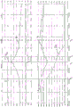
Describe control method of the present invention in detail below with reference to Fig. 8-12.Here, show control signal and gained voltage and/or the electric current of execution mode shown in Figure 3.Input voltage vin is set to 50VDC, and output voltage is adjusted to 350VDC.Switching frequency is approximately 110kHz.
With reference now to Fig. 8.
At first step, for series resonance DC/DC transducer, switch periods TP is defined as the time from time T start to time Tend.Switch periods TP comprises the first half period TA from Tstart to time Tcenter and the second half period TB from time T center to time Tend.Be labeled as follow-up switch periods TP+1 the next switching time after the switch periods TP.
As above, the resonance frequency of series resonance DC/DC transducer is defined by element (capacitor and the inductor) characteristic of inductor arrangement (ID or TD) and resonant circuit RC.
Switch periods TP and then switching frequency can by control circuit be controlled to be greater than, be equal to or less than resonance frequency.Therefore, switch periods TP and resonance frequency are irrelevant.
Among Fig. 8, as apparent from following explanation, correlation time, T0(equaled Tstart) equal Tend to T8() the first switch periods TP be illustrated by the broken lines, also defined a plurality of time intervals.Time T 8(equals Tend) be the starting point (being time T0(TP+1) of follow-up switch periods TP+1).Here, time T 4 equals Tcenter, but time interval T0 – is T1, the length of T1-T2, T2-T3, T3-T4, T4-T5, T5-T6, T6-T7, T7-T8 all is not equal to each other.
Basically the duty ratio of all switches set all is 50%, mean during almost half switch periods, switch has the control signal that needs switch to be in conducted state ON, and during almost half switch periods, switch has the control signal that needs switch to be in non-conduction condition OFF.Switches set is independently controlled to have different the delay still synchronously.
First group of switch S 1sc1 of the first switching circuit SC1; It is closed that S1sc1, S4sc1 are controlled as that the Tstart that deducts time interval Δ TAE1 since the first half period TA begins, and wherein time interval Δ TAE1 is arranged on the end of the first half period TA.First group of switch S 1sc1 of the first switching circuit SC1; S1sc1, S4sc1 are controlled as in the second half period TB and disconnect.Time interval Δ TAE1 in the present embodiment stops in time T 3 beginnings and in time T 4.
Second group of switch S 2sc1 of the first switching circuit SC1; It is closed that S2sc1, S3sc1 are controlled as that the Tcenter that deducts time interval Δ TBE1 since the second half period TB begins, and wherein time interval Δ TBE1 is arranged on the end of the second half period TB; Second group of switch S 2sc1 of the first switching circuit SC1; S2sc1, S2sc1 are controlled as in the first half period TA and disconnect.Time interval Δ TBE1 in the present embodiment stops in time T 7 beginnings and in time T 8.
First group of switch S 1sc1 of the first switching circuit SC1; S1sc1, S4sc1 and second group of switch S 2sc1; S2sc1, S3sc1 are controlled as in time interval Δ TAE1 and time interval Δ TBE1 and disconnect.
Time interval Δ TAE1 forms very first time interval T sc1off1, and wherein first and second of first switching circuit groups of switches disconnect.Time interval Δ TBE1 forms second time interval Tsc1off2, and wherein first and second of the first switching circuit SC1 groups of switches disconnect.
First group of switch S 1sc2 of second switch circuit SC2; S1sc2, S4sc2 are controlled as and deduct time interval Δ TAS1 and deduct in the time interval Δ TAE2 at the first half period TA is closed, wherein time interval Δ TAS1 be arranged on the beginning of the first half period TA and wherein time interval Δ TAE2 be arranged on the end of the first half period TA.First group of switch S 1sc2 of second switch circuit SC2; S1sc2, S4sc2 are controlled as in the second half period TB and disconnect.Time interval Δ TAS1 in the present embodiment stops in time T 0 beginning with in time T 1.Time interval Δ TAE2 in the present embodiment stops in time T 2 beginnings with in time T 4.
Second group of switch S 2sc2 of second switch circuit SC2; S2sc2, S3sc2 are controlled as deducting time interval Δ TBS1 and deducting in the time interval Δ TBE2 at the second half period TB and remain closed, wherein time interval Δ TBS1 is arranged on the beginning of the second half period TB, and wherein time interval Δ TBE2 is arranged on the end of the second half period TB.Second group of switch S 2sc2 of second switch circuit SC2; S2sc2, S3sc2 are controlled as in the first half period TA and disconnect.Time interval Δ TBS1 in the present embodiment stops in time T 4 beginnings with in time T 5.Time interval Δ TBE2 in the present embodiment stops in time T 6 beginnings with in time T 8.
First group of switch S 1sc1 of second switch circuit SC2; S1sc2, S4sc2 and second group of switch S 2sc2; S2sc2, S3sc2 are controlled as in time interval Δ TAS1, Δ TAE2, Δ TBS1 and Δ TBE2 and disconnect.
Time interval Δ TAE2 and Δ TBS1 form the continuous time interval Tsc2off1 from time T 2 to time T5, and wherein first and second of second switch circuit SC2 groups of switches disconnect.Time interval Δ TBE2 and Δ TAS1(TP+1) (time interval Δ TAS1 of follow-up switch periods TP+1 just) form from time T 6 to time T1(TP+1) (just, the time instance T1 of follow-up switch periods TP+1) continuous time interval Tsc2off2, wherein first and second of second switch circuit SC2 groups of switches all disconnect.
Following table 1 shows the state of first and second groups of switches of first switching circuit among the switch periods TP.Zero-time and the concluding time in each time interval have also been provided.

Table1: the closure/off-state of first and second groups of switches of the first switching circuit SC1.
Following table 2 shows the first and second groups of on off states of second switch circuit SC2 among the switch periods TP.Zero-time and the concluding time in each time interval have also been provided.

Table2: the closure/off-state of first and second groups of switches of second switch circuit SC2.
Time interval Tsc1off1 and time interval Tsc2off1 are at least part of overlapping, i.e. time interval Tsc1off1 beginning or time interval Tsc2off1 beginning before time interval Tsc1off1 finishes before time interval Tsc2off1 finishes.In addition, time interval Tsc1off2 and time interval Tsc2off2 are at least part of overlapping, i.e. time interval Tsc1off2 beginning or time interval Tsc2off2 beginning before time interval Tsc1off2 finishes before time interval Tsc2off2 finishes.The switch of the switch of the synchronous first switching circuit SC1 and second switch circuit SC2 in this way.
In the present embodiment, the length of time interval Tsc2off1 equals the length of time interval Tsc2off2, and the length of time interval Tsc1off1 equals the length of time interval Tsc1off2.
In the above-described embodiment, time interval Tsc2off1 and Tsc2off2 are longer than time interval Tsc1off1 and Tsc1off2.Yet it can have the identical duration, or time interval Tsc1off can be longer than time interval Tsc2off.This depend on realize the required time of zero voltage switch (ZVS) in the switching circuit and just also depending on first and negative DC terminal between voltage and second voltage just and between the negative DC terminal.
In the above-described embodiment, the center of time interval Tsc1off1 is controlled as the center that approaches or equal time interval Tsc2off1, and the center of time interval Tsc1off2 is controlled as the center that approaches or equal time interval Tsc2off2.
When as shown in Figure 8, high capacity is to fully loaded closure all switches are kept zero voltage switch.
Among Fig. 9, the voltage V10 of node 10 and the V20 of node 20 are high before time T 2 examples, therefore first group of switch S 1sc1, S4sc1(SC1) and first group of S1sc2(SC1) all conductings, and switch S 2sc1, S3sc1(SC1 second group) and second group of S2sc2(SC2) not conductings.
At time instance T2, first group of switch S 1sc2 of second switch circuit SC2 is disconnected.At the time instance place, when electric current I s just becomes, then can make the voltage of node 10 from high step-down by the output capacitance discharge in first group and the second group of switch in the second switch circuit.Order second group of switch S 2sc2 of second switch circuit in time T 5 place's closures, and then to approach zero voltage closure, can not produce any significant switching losses, so be known as zero voltage switch (ZVS).
Because Ip is for just, disconnect first group of switch S 1sc1 and S4sc1 will cause the voltage of node 20 to uprise from low fast from the voltage of high step-down and node 22 fast in time T 3, this is that output capacitance fast charge/discharge by first combination of first switching circuit and second group of switch S 1sc1, S3sc1 and S2sc1, S4sc1 causes.Order second group of switch S 2sc1 of the first switching circuit SC1 and S3sc1 in the T4 closure, and then with the voltage closure near null value, can not produce any significant switching losses, so be known as ZVS.
Note, in the present embodiment, be longer than disconnection S1sc1 at the time interval T2 that disconnects between S1sc2 and the closed S2sc2 to T5, S4sc1 and closed S2sc1, the time interval T3 of S3sc1 is to T4, because the time of the 350V voltage Vout current transformation (commutate) of second switch circuit SC2 is longer than the 50V voltage Vin of the first switching circuit SC1.
As shown in figure 10, all switches keep ZVS when low load or unloaded closure.With reference now to Figure 11.
Before time instance T2, the voltage V10 of node 10 and the voltage V20 of node 20 are high, so switch S 1sc1, S4sc1 and all conductings of S1sc2.
Switch S 1sc2 disconnects at time instance T2.Therefore electric current I s can make V10 from high step-down by the output capacitance discharge of switch S 1sc2 and S2sc2 for just.
During period of time T 2 to T3, owing to change by the voltage of resonant inductor Lrc, so electric current I s decay.Yet, the magnetizing current I among the winding L s
LMStill increase, and and then be reflected into elementary winding L
p, and cause electric current I
pIncrease.Because I
pIncrease and for just, the voltage V20 that cut-off switch S1sc1 and S4sc1 cause node 20 uprises from low fast from the voltage V22 of high step-down and node 22 fast, and this is that output capacitance fast charge/discharge by switch S 1sc1, S3sc1 and S2sc1, S4sc1 causes.
Can control output voltage V out by changing switching frequency.This is illustrated in Figure 12, and wherein output voltage V out can change with different switching frequencies for different loads.Can control the ZVS operation of all switches by suitable delay, namely above and time interval Tsc1off1, Tsc1off2, Tsc2off1 and Tsc2off2 between the switch example shown in Fig. 8, table 2 and the table 3.
Can control between series resonance DC/DC transducer the one DC terminal T1P, the T1N relation between the voltage between the voltage and series resonance DC/DC transducer the 2nd DC terminal T2P, T2N by the length that changes switch periods TP.
Can control direction by the flow of power of series resonance DC/DC transducer by the length that changes switch periods TP.Therefore series resonance DC/DC transducer can be controlled as two-way series resonance DC/DC transducer.
The switch of the first and second switching circuit SC1, SC2 is controlled as by controlling first and second switching circuits has fixed switching frequency near series resonance frequency, zero voltage switch ZVS is provided when switch closure and approximate zero current switch ZCS is provided when switch disconnects.
By being that a DC terminal all voltages in the nominal operation scope carry out switch at operating point with series resonance frequency or near the frequency of series resonance frequency, can control the switch of the first and second switching circuit SC1, SC2.
By being that all load states at the second terminal place carry out switch at operating point with series resonance frequency or near the frequency of series resonance frequency, can control the switch of the first and second switching circuit SC1, SC2.
Ups system with series connection DC/DC resonance converter
In above-mentioned introduction, illustrated that the typical case of series resonance DC/DC transducer uses.In typical ups system, exist one to be used for the common control system that ups system comprises all parts of series resonance DC/DC transducer.For example, common control circuit can comprise the Status Flag signal, as the designator to the direction of the flow of power by two-way DC/DC transducer.
In addition, control circuit comprises for induction the one DC terminal T1P, T1N and the 2nd DC terminal T2P, the electric current at T2N place and/or the transducer of voltage.
In first operator scheme, Status Flag signal indication electric power should flow to the 2nd DC terminal T2P, T2N from a DC terminal T1P, T1N.Here, control circuit is controlled electric current and/or the voltage of the 2nd DC terminal T2P, T2N based on the predetermined reference signal that is used for first operator scheme.
In second operator scheme, Status Flag signal indication electric power should flow to a DC terminal T1P, T1N from the 2nd DC terminal T2P, T2N.Here, control circuit is controlled electric current and/or the voltage of a DC terminal T1P, T1N based on the predetermined reference signal that is used for second operator scheme.
As above, series resonance DC/DC transducer can be as the DC/DC transducer of ups system, and as shown in Figure 1, wherein its DC terminal T1P, T1N are connected to battery, and its 2nd DC terminal T2P, T2N are connected to DC bus (not shown).
When detecting fault in the AC main line, the Status Flag signal can be switched to first operator scheme.In this case, electric power should be transferred to the DC bus that is connected to the 2nd DC terminal from the battery that is connected to a DC terminal.Here, as long as battery supply allows, control circuit is controlled the voltage at the 2nd DC terminal T2P, T2N place and/or the predetermined level that electric current keeps being suitable for being input to the DC/AC transducer.
When the AC main line was worked again, the Status Flag signal can switch to second operator scheme, then from the DC bus to battery supplied electric power to battery charge.Here, control circuit is controlled the voltage of a DC terminal T1P, T1N and/or the predetermined level that electric current keeps being suitable for being transfused to battery.
The Status Flag signal can have indication does not have electric current should be transmitted through the 3rd operator scheme of two-way DC/DC transducer.In this operator scheme, all switches all should disconnect.In this operator scheme, do not have fault in the AC main line, and battery is filled.
The another kind application that is used for series resonance DC/DC transducer is the recycling be used to the energy that is stored in the battery storage device.
Conclusion
Efficient according to the series resonance DC/DC transducer of Fig. 3 is measured.Figure 12 shows test result.In test, show two efficiency curves, first curve shows efficient with the output power function of circuit with 50V input voltage vin, and second curve shows efficient with the output power function of circuit with 48V input voltage vin.Output voltage V out control is at 355V.
As can be seen, in the power output area of 2200W, efficient is higher than 96% at about 400W.Maximum power efficiency is higher than 97.5%.Only the have an appointment DC/DC transducer of 92% prior art of this efficient of mentioning in relatively introducing is significant a raising.
Claims (8)
1. a method that is used for control series resonance DC/DC transducer comprises the following steps:
Be the switch periods TP of described series resonance DC/DC transducer definition from time T start to time Tend; Wherein, described switch periods TP comprises the first half period TA from time T start to time Tcenter and the second half period TB from time T center to time Tend, and defines follow-up switch periods TP+1 after described switch periods TP;
Control first group of switch (S1sc1 of first switching circuit (SC1); S1sc1, S4sc1) to begin be closed for the beginning Tstart that deducts time interval Δ TAE1 from the described first half period TA, wherein, described time interval Δ TAE1 is arranged on the end of the described first half period TA;
Control second group of switch (S2sc1 of described first switching circuit (SC1); S2sc1, S3sc1) to begin be closed for the beginning Tcenter that deducts time interval Δ TBE1 from the described second half period TB, wherein, described time interval Δ TBE1 is arranged on the end of the described second half period TB;
Control described first group of switch (S1sc1 of described first switching circuit (SC1); S1sc1, S4sc1) and described second group of switch (S2sc1; S2sc1, S3sc1) in described time interval Δ TAE1 and described time interval Δ TBE1, disconnect;
First group of switch (S1sc2 of control second switch circuit (SC2); S1sc2, S4sc2) to deduct time interval Δ TAS1 and deduct in cycle of time interval Δ TAE2 at the described first half period TA be closed, wherein, described time interval Δ TAS1 is arranged on the beginning of the described first half period TA, and wherein, described time interval Δ TAE2 is arranged on the end of the described first half period TA;
Control second group of switch (S2sc2 of described second switch circuit (SC2); S2sc2, S3sc2) to deduct time interval Δ TBS1 and deduct in cycle of time interval Δ TBE2 at the described second half period TB be closed, wherein, described time interval Δ TBS1 is arranged on the beginning of the described second half period TB, and wherein, described time interval Δ TBE2 is arranged on the end of the described second half period TB;
Control described first group of switch (S1sc2 of described second switch circuit (SC2); S1sc2, S4sc2) and described second group of (S2sc2; S2sc2, S3sc2) in described time interval Δ TAS1, Δ TAE2, Δ TBS1 and Δ TBE2, disconnect;
Wherein, described time interval Δ TAE1 forms very first time interval T sc1off1, described first group of switch and described second group of switch of wherein said first switching circuit (SC1) disconnect, and wherein, described time interval Δ TBE forms second time interval Tsc1off2, and described first group of switch and described second group of switch of wherein said first switching circuit (SC1) all disconnect;
Wherein, described time interval Δ TAE2 and Δ TBS1 form continuous time interval Tsc2off1, and described first group of switch and described second group of switch of wherein said second switch circuit (SC2) disconnect; And wherein, the time interval Δ TAS1(TP+1 of described time interval Δ TBE2 and described follow-up switch periods TP+1) form continuous time interval Tsc2off2, described first group of switch and described second group of switch of wherein said second switch circuit (SC2) disconnect;
Wherein, described time interval Tsc1off1 and described time interval Tsc2off1 are overlapping, and wherein, described time interval Tsc1off2 and described time interval Tsc2off2 are overlapping.
2. method according to claim 1, wherein, described method comprises that the center of controlling described interval T sc1off1 approaches or equal the center of described time interval Tsc2off1, and the center of controlling described interval T sc1off2 approaches or equal the center of described time interval Tsc2off2.
3. method according to claim 1 and 2, wherein, described method comprises a DC terminal (T1P who controls described series resonance DC/DC transducer by the length that changes described switch periods TP, the 2nd DC terminal (T2P, T2N) relation between the voltage between of the voltage T1N) and described series resonance DC/DC transducer.
4. according to any described method in the claim 1 to 3, wherein, described method comprises by changing described switch periods TP controls direction by the flow of power of described series resonance DC/DC transducer.
5. according to any described method in the claim 1 to 4, wherein, described method comprises by controlling described first switching circuit and described second switch circuit having fixed switching frequency close to described series resonance frequency, (SC1, switch SC2) provide zero voltage switch (ZVS) and approximate Zero Current Switch (ZCS) are provided when switch disconnects when switch closure to control described first switching circuit and described second switch circuit.
6. method according to claim 5, wherein, by with described series resonance frequency or near the frequency of described series resonance frequency all voltages in the nominal operation scope on the described DC terminal being carried out switch at operating point, control described first switching circuit and described second switch circuit (SC1, switch SC2).
7. method according to claim 5, wherein, by with described series resonance frequency or near the frequency of described series resonance frequency all load states at described the 2nd DC terminal place being carried out switch at operating point, control described first switching circuit and described second switch circuit (SC1, switch SC2).
8. series resonance DC/DC transducer comprises:
The one DC terminal (T1P, T1N);
The 2nd DC terminal (T2P, T2N);
Inductor arrangement (ID; TD);
First switching circuit (SC1) is connected a described DC terminal (T1P, T1N) and described inductor arrangement (ID; TD) between, wherein, described first switching circuit (SC1) comprises first group of switch (S1sc1; S1sc1, S4sc1) and second group of switch (S2sc1; S2sc1, S3sc1);
Second switch circuit (SC2) and resonant circuit (RC), (T2P is T2N) with described inductor arrangement (ID to be connected described the 2nd DC terminal; TD) between, wherein, described second switch circuit (SC2) comprises first group of switch (S1sc2; S1sc2, S4sc2) and second group of switch (S2sc2; S2sc2, S3sc2);
Control circuit is used for controlling described first switching circuit and described second switch circuit (SC1, switches set SC2) according to any one described method of claim 1 to 7.
Applications Claiming Priority (5)
| Application Number | Priority Date | Filing Date | Title |
|---|---|---|---|
| US40746610P | 2010-10-28 | 2010-10-28 | |
| GB1018262.4A GB2484971A (en) | 2010-10-28 | 2010-10-28 | Control of a bidirectional series resonant DC/DC converter |
| GB1018262.4 | 2010-10-28 | ||
| US61/407,466 | 2010-10-28 | ||
| PCT/EP2011/068643 WO2012055862A2 (en) | 2010-10-28 | 2011-10-25 | Method for controlling a series resonant dc/dc converter |
Publications (2)
| Publication Number | Publication Date |
|---|---|
| CN103190064A true CN103190064A (en) | 2013-07-03 |
| CN103190064B CN103190064B (en) | 2016-04-13 |
Family
ID=43401483
Family Applications (1)
| Application Number | Title | Priority Date | Filing Date |
|---|---|---|---|
| CN201180052309.XA Active CN103190064B (en) | 2010-10-28 | 2011-10-25 | For controlling the method for series resonance DC/DC transducer |
Country Status (13)
| Country | Link |
|---|---|
| US (1) | US8593831B2 (en) |
| EP (1) | EP2633610B1 (en) |
| JP (1) | JP5913336B2 (en) |
| KR (1) | KR101840315B1 (en) |
| CN (1) | CN103190064B (en) |
| BR (1) | BR112013010456A2 (en) |
| CA (1) | CA2811183A1 (en) |
| CO (1) | CO6801653A2 (en) |
| EA (1) | EA027919B1 (en) |
| GB (1) | GB2484971A (en) |
| MY (1) | MY164460A (en) |
| SG (1) | SG189006A1 (en) |
| WO (1) | WO2012055862A2 (en) |
Cited By (4)
| Publication number | Priority date | Publication date | Assignee | Title |
|---|---|---|---|---|
| CN103929064A (en) * | 2014-03-24 | 2014-07-16 | 江苏固德威电源科技有限公司 | Isolated two-way DC/DC converter and control method thereof |
| WO2015109862A1 (en) * | 2014-01-21 | 2015-07-30 | 华为技术有限公司 | Power supply converter |
| CN104836325A (en) * | 2014-02-12 | 2015-08-12 | 艾默生网络能源有限公司 | Switching control methods of uninterruptible power supply, switching control devices of uninterruptible power supply and uninterruptible power supply system |
| CN104868776A (en) * | 2015-05-12 | 2015-08-26 | 江苏固德威电源科技有限公司 | Bidirectional control driving circuit applied to energy storage inverter |
Families Citing this family (18)
| Publication number | Priority date | Publication date | Assignee | Title |
|---|---|---|---|---|
| WO2011014482A1 (en) | 2009-07-27 | 2011-02-03 | Magna Electronics Inc. | Parking assist system |
| KR101449120B1 (en) * | 2012-09-06 | 2014-10-13 | 엘지이노텍 주식회사 | The power supply device |
| JP5995139B2 (en) * | 2012-10-12 | 2016-09-21 | 富士電機株式会社 | Bidirectional DC / DC converter |
| US9356523B2 (en) * | 2012-12-28 | 2016-05-31 | Panasonic Intellectual Property Management Co., Ltd. | DC-to-DC converter |
| GB2524992A (en) | 2014-04-08 | 2015-10-14 | Eltek As | Electic multi-mode power converter module and power system |
| US10328932B2 (en) | 2014-06-02 | 2019-06-25 | Magna Electronics Inc. | Parking assist system with annotated map generation |
| DE102015002687A1 (en) * | 2015-03-04 | 2016-09-08 | Witech GmbH | Method of inductive power transmission |
| WO2016157963A1 (en) * | 2015-03-30 | 2016-10-06 | 株式会社村田製作所 | Switching power supply device |
| CN104852586B (en) * | 2015-05-27 | 2017-09-22 | 深圳科士达科技股份有限公司 | A kind of bidirectional DC/DC converter |
| EP3104509A1 (en) * | 2015-06-09 | 2016-12-14 | Constructions Electroniques + Telecommunications | Dual bridge dc/dc power converter |
| US10078789B2 (en) | 2015-07-17 | 2018-09-18 | Magna Electronics Inc. | Vehicle parking assist system with vision-based parking space detection |
| US9973099B2 (en) | 2015-08-26 | 2018-05-15 | Futurewei Technologies, Inc. | AC/DC converters with wider voltage regulation range |
| WO2017065750A1 (en) * | 2015-10-13 | 2017-04-20 | Nissan Motor Co., Ltd. | Power converter |
| EP3403321B1 (en) | 2016-01-15 | 2020-05-06 | General Electric Company | System and method for operating a dc to dc power converter |
| US10177671B2 (en) * | 2016-12-07 | 2019-01-08 | Carl David Klaes | Modified dual active half bridge DC/DC converter with transformer DC bias |
| EP3577753A1 (en) * | 2017-01-31 | 2019-12-11 | Vestas Wind Systems A/S | Dc-dc converter and dc-dc conversion method |
| GB2566479B (en) * | 2017-09-14 | 2019-10-23 | Eltek As | DC-DC Converter |
| CN109194130B (en) * | 2018-09-06 | 2020-11-17 | 南京南瑞继保电气有限公司 | Unidirectional direct-current voltage conversion device and system and control method thereof |
Citations (3)
| Publication number | Priority date | Publication date | Assignee | Title |
|---|---|---|---|---|
| US6370050B1 (en) * | 1999-09-20 | 2002-04-09 | Ut-Batelle, Llc | Isolated and soft-switched power converter |
| US20080074905A1 (en) * | 2006-09-22 | 2008-03-27 | Kabushiki Kaisha Toyota Jidoshokki | Method for Controlling Bidirectional DC-DC Converter |
| CN101378232A (en) * | 2007-08-28 | 2009-03-04 | 日立计算机机器株式会社 | Bi-directional dc-dc converter and method for controlling the same |
Family Cites Families (9)
| Publication number | Priority date | Publication date | Assignee | Title |
|---|---|---|---|---|
| US4953068A (en) * | 1989-11-08 | 1990-08-28 | Unisys Corporation | Full bridge power converter with multiple zero voltage resonant transition switching |
| JP2976603B2 (en) | 1991-07-23 | 1999-11-10 | 日本電気株式会社 | Series resonant converter control circuit |
| JP2003259643A (en) * | 2002-03-04 | 2003-09-12 | Orc Mfg Co Ltd | Current resonance type soft switching power circuit |
| JP4274353B2 (en) * | 2003-03-13 | 2009-06-03 | 本田技研工業株式会社 | Bidirectional DC-DC converter |
| JP4280976B2 (en) | 2003-04-10 | 2009-06-17 | 横河電機株式会社 | Switching power supply |
| KR100547289B1 (en) * | 2005-05-18 | 2006-01-26 | 주식회사 피에스텍 | Synchronous rectifier type series resonant converter for operating in intermittence mode |
| JP4527616B2 (en) * | 2005-06-24 | 2010-08-18 | 株式会社日立製作所 | Insulated resonant bidirectional DC / DC converter and control method thereof |
| JP5065188B2 (en) | 2008-05-23 | 2012-10-31 | オリジン電気株式会社 | Series resonant converter |
| JP5278224B2 (en) * | 2008-12-08 | 2013-09-04 | 富士電機株式会社 | Switching power supply device and switching power supply control circuit |
-
2010
- 2010-10-28 GB GB1018262.4A patent/GB2484971A/en not_active Withdrawn
-
2011
- 2011-10-25 US US13/821,571 patent/US8593831B2/en active Active
- 2011-10-25 SG SG2013019435A patent/SG189006A1/en unknown
- 2011-10-25 MY MYPI2013000895A patent/MY164460A/en unknown
- 2011-10-25 CN CN201180052309.XA patent/CN103190064B/en active Active
- 2011-10-25 JP JP2013535402A patent/JP5913336B2/en not_active Expired - Fee Related
- 2011-10-25 CA CA2811183A patent/CA2811183A1/en not_active Abandoned
- 2011-10-25 EP EP11774061.3A patent/EP2633610B1/en active Active
- 2011-10-25 BR BR112013010456A patent/BR112013010456A2/en not_active IP Right Cessation
- 2011-10-25 EA EA201390591A patent/EA027919B1/en not_active IP Right Cessation
- 2011-10-25 WO PCT/EP2011/068643 patent/WO2012055862A2/en active Application Filing
- 2011-10-25 KR KR1020137013570A patent/KR101840315B1/en active IP Right Grant
-
2013
- 2013-05-17 CO CO13122455A patent/CO6801653A2/en not_active Application Discontinuation
Patent Citations (3)
| Publication number | Priority date | Publication date | Assignee | Title |
|---|---|---|---|---|
| US6370050B1 (en) * | 1999-09-20 | 2002-04-09 | Ut-Batelle, Llc | Isolated and soft-switched power converter |
| US20080074905A1 (en) * | 2006-09-22 | 2008-03-27 | Kabushiki Kaisha Toyota Jidoshokki | Method for Controlling Bidirectional DC-DC Converter |
| CN101378232A (en) * | 2007-08-28 | 2009-03-04 | 日立计算机机器株式会社 | Bi-directional dc-dc converter and method for controlling the same |
Non-Patent Citations (1)
| Title |
|---|
| XIAODONG LI等: "Analysis and Design of High-Frequency Isolated Dual-Bridge Series Resonant DC/DC Converter", 《IEEE TRANSACTIONS ON POWER ELECTRONICS》, vol. 25, no. 4, 30 April 2010 (2010-04-30) * |
Cited By (6)
| Publication number | Priority date | Publication date | Assignee | Title |
|---|---|---|---|---|
| WO2015109862A1 (en) * | 2014-01-21 | 2015-07-30 | 华为技术有限公司 | Power supply converter |
| CN104836325A (en) * | 2014-02-12 | 2015-08-12 | 艾默生网络能源有限公司 | Switching control methods of uninterruptible power supply, switching control devices of uninterruptible power supply and uninterruptible power supply system |
| CN103929064A (en) * | 2014-03-24 | 2014-07-16 | 江苏固德威电源科技有限公司 | Isolated two-way DC/DC converter and control method thereof |
| CN103929064B (en) * | 2014-03-24 | 2016-09-28 | 江苏固德威电源科技股份有限公司 | The two-way DC/DC changer of a kind of isolation and control method thereof |
| CN104868776A (en) * | 2015-05-12 | 2015-08-26 | 江苏固德威电源科技有限公司 | Bidirectional control driving circuit applied to energy storage inverter |
| CN104868776B (en) * | 2015-05-12 | 2016-10-12 | 江苏固德威电源科技股份有限公司 | It is applied to the double-direction control drive circuit of energy storage inverter |
Also Published As
| Publication number | Publication date |
|---|---|
| EP2633610B1 (en) | 2014-09-03 |
| KR20130082166A (en) | 2013-07-18 |
| GB201018262D0 (en) | 2010-12-15 |
| CA2811183A1 (en) | 2012-03-05 |
| EP2633610A2 (en) | 2013-09-04 |
| EA201390591A1 (en) | 2013-10-30 |
| WO2012055862A2 (en) | 2012-05-03 |
| KR101840315B1 (en) | 2018-03-20 |
| WO2012055862A3 (en) | 2012-06-21 |
| EA027919B1 (en) | 2017-09-29 |
| CN103190064B (en) | 2016-04-13 |
| JP5913336B2 (en) | 2016-04-27 |
| CO6801653A2 (en) | 2013-11-29 |
| US8593831B2 (en) | 2013-11-26 |
| MY164460A (en) | 2017-12-15 |
| JP2013545426A (en) | 2013-12-19 |
| BR112013010456A2 (en) | 2017-04-18 |
| GB2484971A (en) | 2012-05-02 |
| US20130208512A1 (en) | 2013-08-15 |
| SG189006A1 (en) | 2013-05-31 |
Similar Documents
| Publication | Publication Date | Title |
|---|---|---|
| CN103190064B (en) | For controlling the method for series resonance DC/DC transducer | |
| EP2274813B1 (en) | A power converter system that operates efficiently over a range of load conditions | |
| Park et al. | Nonisolated high step-up boost converter integrated with sepic converter | |
| Park et al. | High step-up boost converter integrated with a transformer-assisted auxiliary circuit employing quasi-resonant operation | |
| Hsieh et al. | An interleaved boost converter with zero-voltage transition | |
| EP2670039B1 (en) | Quasi resonant push-pull converter and control method thereof | |
| CN104143919A (en) | Bidirectional direct-current converter | |
| CN104052296A (en) | System And Method For A Switched-mode Power Converter | |
| Karshenas et al. | Basic families of medium-power soft-switched isolated bidirectional dc-dc converters | |
| WO2012055869A2 (en) | Series resonant dc/dc converter | |
| KR20180004675A (en) | Bidirectional Converter with Auxiliary LC Resonant Circuit and Operating Method thereof | |
| TW201541838A (en) | Flyback active clamping power converter | |
| Sun et al. | A novel LLC integrated three-port dc-dc converter for stand-alone PV/battery system | |
| CN104638932A (en) | Multi-resonant converter | |
| CN113541486A (en) | Interleaved diode capacitor network high-gain ZVT (zero voltage zero volt) direct current converter and auxiliary circuit | |
| Lin et al. | Analysis of an integrated flyback and zeta converter with active clamping technique | |
| Seong et al. | Novel dual inductor-fed DC-DC converter integrated with parallel boost converter | |
| CN114930703A (en) | DC power converter | |
| Cheng et al. | A novel interleaved flyback-typed converter with ZVS operation | |
| Lai et al. | A general-purpose three-phase dc-dc converter building block for fuel cell applications | |
| Kalahasthi et al. | A high‐gain low‐ripple DC–DC converter for micro‐grid applications | |
| Bian et al. | A high performance boost converter with voltage multiplier | |
| Yeşilyurt | Hybrid dual output LLC converter with low slave output rectifier current | |
| OA16581A (en) | Method for controlling a series resonant DC/DC converter. | |
| Piegari et al. | Zero voltage switching configuration of a dual inductor current fed DC/DC converter |
Legal Events
| Date | Code | Title | Description |
|---|---|---|---|
| C06 | Publication | ||
| PB01 | Publication | ||
| C10 | Entry into substantive examination | ||
| SE01 | Entry into force of request for substantive examination | ||
| C14 | Grant of patent or utility model | ||
| GR01 | Patent grant |