CN101266529A - Display device and electronic device - Google Patents
Display device and electronic device Download PDFInfo
- Publication number
- CN101266529A CN101266529A CNA2008100852203A CN200810085220A CN101266529A CN 101266529 A CN101266529 A CN 101266529A CN A2008100852203 A CNA2008100852203 A CN A2008100852203A CN 200810085220 A CN200810085220 A CN 200810085220A CN 101266529 A CN101266529 A CN 101266529A
- Authority
- CN
- China
- Prior art keywords
- light
- image
- light source
- display device
- indicating mechanism
- Prior art date
- Legal status (The legal status is an assumption and is not a legal conclusion. Google has not performed a legal analysis and makes no representation as to the accuracy of the status listed.)
- Pending
Links
Images


Classifications
-
- G—PHYSICS
- G06—COMPUTING; CALCULATING OR COUNTING
- G06F—ELECTRIC DIGITAL DATA PROCESSING
- G06F3/00—Input arrangements for transferring data to be processed into a form capable of being handled by the computer; Output arrangements for transferring data from processing unit to output unit, e.g. interface arrangements
- G06F3/01—Input arrangements or combined input and output arrangements for interaction between user and computer
- G06F3/03—Arrangements for converting the position or the displacement of a member into a coded form
- G06F3/041—Digitisers, e.g. for touch screens or touch pads, characterised by the transducing means
- G06F3/042—Digitisers, e.g. for touch screens or touch pads, characterised by the transducing means by opto-electronic means
-
- G—PHYSICS
- G06—COMPUTING; CALCULATING OR COUNTING
- G06F—ELECTRIC DIGITAL DATA PROCESSING
- G06F3/00—Input arrangements for transferring data to be processed into a form capable of being handled by the computer; Output arrangements for transferring data from processing unit to output unit, e.g. interface arrangements
- G06F3/01—Input arrangements or combined input and output arrangements for interaction between user and computer
- G06F3/03—Arrangements for converting the position or the displacement of a member into a coded form
- G06F3/041—Digitisers, e.g. for touch screens or touch pads, characterised by the transducing means
- G06F3/0412—Digitisers structurally integrated in a display
Abstract
The invention supplies a display device. A sensor part (204) and a display part are integrated on the image display area (10a) on the TFT array substrate (10). A sensor control circuit part (201) controls the motion of the sensor part (204), and supplies the signals for changing the light intensity of the light source emitted from the backlight (206) to the backlight control circuit part (202). When detecting the indicating mechanism such as finger, the sensor control circuit part (201) processes the data of the image shot with the indicating mechanism, to determine the location of the indicating mechanism.
Description
Technical field
The present invention relates to for example to have touch panel function liquid-crystal apparatus etc. display device and possess this display device and the technical field of the electronic equipment that constitutes.
Background technology
In liquid-crystal apparatus as an example of this display device, proposed to have the display device of so-called touch panel function, wherein, by a plurality of pixel portions or with the pixel portions of any number is one group and by the configuration set optical sensor, can carry out the image demonstration based on the light that sees through that sees through pixel portions, and can be by indicating mechanism to this display device input information.In such display device, the indicating mechanism that the photo detector by optical sensor etc. detects finger or indicating device etc. contacts with the display surface of liquid-crystal apparatus or is mobile on display surface, thereby can be to this display device input information.Photo detector as optical sensor etc. for example uses semiconductor elements such as photodiode.Photodiode is electrically connected with capacity cell, and according to from the variation of display surface to the light income of the light of this display device incident, the quantity of electric charge of accumulating in the capacity cell changes.In this display device, by detecting the voltage between the pair of electrodes that capacity cell had, generate the data of indicating mechanism having been carried out the photographed images of shooting, be taken into the image of indicating mechanism.
In addition, the photo detector of optical sensor etc. for example is set at non-open area that the open area is isolated mutually, promptly image is shown there not be the zone of contributing, show that described open area makes in the viewing area image is shown contributive light transmission in order to avoid hinder image.
In such display device, around the indicating mechanism when bright,, determine the image of indicating mechanism by discerning shadow and its bright zone on every side near display surface or the indicating mechanism that contact with display surface.On the other hand, in such display device, around the indicating mechanism when dark,, determine the image of indicating mechanism by distinguishing detection with outer light by the light of the detection usefulness of indicating mechanism's reflection.
Patent documentation 1: the spy opens the 2004-318819 communique
Patent documentation 2: the spy opens the 2006-238053 communique
But, according to patent documentation 1 and 2 disclosed display device, there is following problems, the detection electric current that flows in the sensor is faint, is difficult to detect accurately according to the variation of the light intensity of the outer light that shines display surface the position of indicating mechanisms such as finger.More specifically be, when indicating mechanism is darker on every side, under the light intensity circlet border of indoor outer light like this, by the light of the detection usefulness of indicating mechanism reflection and outer light light intensity separately equal extent each other mutually, be difficult to discern the light and the outer light of the detection usefulness that reflects by indicating mechanism.Therefore, by detected outer light by sensor, the pairing light of the image of the indicating mechanism that should detect can not detect under the state of being distinguished out with outer light originally, can't determine the position of indicating mechanism accurately.
And, shown in patent documentation 1, according to the technology that the control signal of control sensor action usefulness is controlled, need to add the adjustment circuit of voltage level or the timing adjusting circuit that light is adjusted detection time, therefore, the circuit of the control circuit that the action of sensor is controlled constitutes and becomes complicated.
Also have, in possessing the display device such as liquid-crystal apparatus of touch panel function, in order to improve the input precision of information, at the environmental impact that is not used this display device, can determine accurately to contact or the technology requirement height of the position of the indicating mechanism of close finger etc. with display surface.
Summary of the invention
The present invention realizes in view of the above problems, for example with provide can not make the control circuit that the action of sensor is controlled complicated and can determine with high precision indicating mechanisms such as finger the position display device such as liquid-crystal apparatus and possess such display device and the electronic equipment that constitutes is a problem.
For solving above-mentioned problem, display device of the present invention comprises: light source, its from by the rear side of the display surface of indicating mechanism indication towards described display surface, have the multi beam light source light of different mutually light intensities with different pulsed exposure mutually; Testing agency, it is arranged on described rear side, and the multi beam reflected light that is reflected by described indicating mechanism in the described multi beam light source light is detected; With definite mechanism, its calculate based on a branch of reflected light that described multi beam reflected light comprised and the brightness data of the first definite image with based on other catoptrical each bundles of multi beam that have the light intensity different in the described multi beam reflected light and the difference value of the brightness data of definite a plurality of second images with described a branch of catoptrical light intensity, and, determine the position of described indicating mechanism based on each of each a plurality of the 3rd images of determining of a plurality of difference values of calculating according to this.
According to display device of the present invention, when it moves, light source from by the rear side of the display surface of indicating mechanisms such as people's finger or indicating device indication towards described display surface, have the multi beam light source light of different mutually light intensities with different pulsed exposure mutually.Light source for example is can be with the flat light source of planar ejaculation light source light towards display surface.Such flat light source also can be by constituting a plurality of point source of light planar alignment.
Testing agency is arranged on rear side, and the multi beam reflected light that is reflected by indicating mechanism in the multi beam light source light is detected.More particularly, from the multi beam light source light that light source penetrates with mutually different timings, restraint the timing of being penetrated according to these multi beam light source light and being reflected towards rear side from display surface as the multi beam reflected light towards each of a part of light source light that contact with display surface or penetrate near the indicating mechanism of display surface.Therefore, be radiated in the multi beam light source light on the display surface with the light source light of indicating mechanism overlapping areas detected respectively as reflected light.
Determine that mechanism is calculated based on a branch of reflected light that the multi beam reflected light comprised and the brightness data of the first definite image with based on other catoptrical each bundles of the multi beam that has the light intensity different in the multi beam reflected light and the difference value of the brightness data of definite a plurality of second images with a branch of catoptrical light intensity, and, determine the position of indicating mechanism based on each of each a plurality of the 3rd images of determining of a plurality of difference values of calculating according to this.
Other catoptrical each bundles of a branch of reflected light and multi beam are at different mutually timings each light by indicating mechanism's reflection from the multi beam light source light of light source ejaculation, and are same with the multi beam light source light, detected by testing agency in mutual different timing.For example, because the multi beam light source light has different light intensity mutually, therefore, do not incide under the certain situation of the light intensity of outer light of display surface being instructed to mechanism around the indicating mechanism, based on other catoptrical each bundles of a branch of reflected light and multi beam and each brightness data of the brightness data of the first definite image and a plurality of other second images is different mutually with blocking.
More particularly, for example, by a branch of reflected light of indicating mechanisms such as finger reflection and the light intensity and the reflection direction of other catoptrical each bundles of multi beam, according to different mutually by the light intensity of each bundle of the multi beam light source light of indicating mechanism reflection, therefore, according to the relative magnitude relationship of the light intensity separately of these reflected light and outer light, each the brightness data that comprises first image of the image section that the profile of indicating mechanism is stipulated and a plurality of second images is also different mutually.On the other hand, the brightness data by detecting the image section that outer light forms is common at these images each other in these first images and a plurality of second image.
Therefore, as hereinafter described,, in the 3rd image, the noise contribution that causes by outer light can be removed, thereby definite precision of the position of determining indicating mechanism can be improved by calculating the difference value of these images.And, according to display device of the present invention, even based on not being instructed to the outer light that mechanism blocks under the image section that the forms situation that the light intensity of light has taken place to change outside, also be cancelled in the 3rd image by the difference value that calculates first image and second image as hereinafter described, thus not can to based on the position of the indicating mechanism of a plurality of the 3rd images really fixed output quota give birth to influence.
And, the image section of the indicating mechanism in each of first image and second image,, reflected light and outer light light intensity separately can determine that therefore the position of the indicating mechanism that display device of the present invention carried out with respect to the relative size of catoptrical light intensity of the light intensity of outer light is definite does not have to influence as long as just there are differences.
Also have, the image section that the profile to indicating mechanism that each comprised of a plurality of the 3rd images is stipulated, it is the overlapped part of image section as the indicating mechanism in each of first image on the basis that the 3rd image is calculated and second image, therefore, can think the image section of the indicating mechanism that the 3rd image is comprised in the 3rd image occupied scope and indicating mechanism the actual scope that occupies is about equally on display surface.
And, according to display device of the present invention, since need not to add optical sensor voltage level the adjustment circuit or adjust the light timing adjusting circuit of detection time, therefore, it is complicated that the circuit of control circuit of the action usefulness of control optical sensor is constituted, and the circuit of display device constituted simplify.
Therefore, according to display device of the present invention,, thereby can irrespectively constitute to determine the position of the indicating mechanism on the display surface with the magnitude relationship of outer light and light source light light intensity separately by simple circuit by each of a plurality of the 3rd images of cross-reference.Therefore, according to display device of the present invention, according to the position of the indicating mechanism that is determined, can be to this display device input information correctly.
In a form of display device of the present invention, the mean value of the centre coordinate of the image section of the described indicating mechanism that each comprised that described definite mechanism also can be by calculating described a plurality of the 3rd images is determined described position.
According to this form, the mean value of the centre coordinate by in a plurality of the 3rd images, calculating the image section that occupies by indicating mechanism in the 3rd image, thus can correctly determine the position of the indicating mechanism's direction in face on the display surface.
In another form of display device of the present invention, also comprise: substrate, it is configured between described light source and the described display surface; With a plurality of pixel portions, constitute the viewing area on the described substrate, described testing agency comprises the photo detector that is formed on non-open area, described non-open area makes the open area of described pixel portions isolate mutually in described viewing area.
According to this form, substrate for example is to be formed with the tft array substrate of pixel switch with semiconductor elements such as TFT, and this display device constitutes and comprises tft array substrate, and the counter substrate of tft array substrate arranged opposite and be clamped in the liquid-crystal apparatus of the liquid crystal layer between these substrates.
A plurality of pixel portions are arranged with array-like on substrate, have constituted the viewing area.In addition, in this form, display surface for example be in the two sides of counter substrate in the face of the surface of a side of liquid crystal layer, display surface with the viewing area overlapping areas in, show the image corresponding with the action of a plurality of pixel portions.Photo detector is optical sensors such as photodiode, is formed on the non-open area that open area that the viewing area makes pixel portions isolates mutually, therefore, can not hinder the image corresponding with the action of a plurality of pixel portions and show.
In another form of display device of the present invention, described light source is also used as the demonstration light source, and the display light that is used for showing the image corresponding with picture signal on described display surface is penetrated in this demonstration with light source.
According to this form, need not to be provided with in addition and penetrate the light source that is used to detect the light that indicating mechanism uses, therefore, the formation of display device is simplified.
In another form of display device of the present invention, described light source constitutes and comprises light emitting diode.
According to this form,, can correctly control the light intensity of light emitting source by the size of control to the input current of light emitting diode input.And, owing to can also correctly control fluorescent lifetime, therefore based on being instructed to mechanism to the reflected light of photo detector reflection and definite first image and a plurality of second images brightness data separately determined by unique according to catoptrical light intensity.
Electronic equipment of the present invention is for solving the display device that above-mentioned problem possesses the invention described above.
According to electronic equipment of the present invention, owing to possess the display device of the invention described above, therefore have touch panel function, and can realize having the various electronic equipments such as mobile phone, electronic notebook, word processor, monitor direct viewing type video tape recorder, workstation, videophone, POS terminal of high-quality demonstration.And, as electronic equipment of the present invention, for example can also realize electrophoretic apparatuss such as Electronic Paper etc.
Such effect of the present invention and advantage thereof can be clear and definite by the embodiment that describes below.
Description of drawings
Fig. 1 is the vertical view of the display device of present embodiment.
Fig. 2 is the II-II ' cut-open view of Fig. 1.
Fig. 3 is the block diagram that the main circuit of the display device of expression present embodiment constitutes.
Fig. 4 is the block diagram that the detailed circuit of expression sensor control circuit portion constitutes.
Fig. 5 is the equivalent electrical circuit of image display area of the display device of present embodiment.
Fig. 6 is an equivalent circuit diagram of having represented the equivalent electrical circuit of sensor part with pixel portions.
Fig. 7 is the vertical view of adjacent a plurality of pixel groups that is formed with the tft array substrate of data line, sweep trace, pixel electrode etc.
Fig. 8 is the VIII-VIII ' cut-open view of Fig. 7.
Fig. 9 is the IX-IX ' cut-open view of Fig. 7.
Figure 10 is the process flow diagram of the location determining method of the indicating mechanism that can be carried out by the display device of present embodiment.
Figure 11 is the skeleton diagram of display device of having represented the light path of light source light, reflected light and outer light with diagram.
Figure 12 is by the concept map of the various images of Flame Image Process from conceptive expression sensor control circuit portion.
Figure 13 is a concept map of having represented to have each light source beam light of different mutually light intensities along time shaft with diagram.
Figure 14 is the variation of concept map shown in Figure 12.
Figure 15 is the concept map of the notion of the principle that will remove by the noise that image was comprised that photodiode is obtained with diagram expression.
Figure 16 is the stereographic map of an example of having represented the electronic equipment of present embodiment.
Figure 17 is another routine stereographic map of having represented the electronic equipment of present embodiment.
Among the figure: the 1-liquid-crystal apparatus; The 10-TFT array base palte; The 72-pixel portions; 201-sensor control circuit portion; The 206-backlight; The 212-photodiode.
Embodiment
Below, with reference to accompanying drawing, each embodiment of display device of the present invention and electronic equipment is described.
<1: display device 〉
<1-1: the integral body of display device constitutes 〉
At first, see figures.1.and.2, the integral body as the liquid-crystal apparatus 1 of the embodiment of " display device " of the present invention is constituted describe.Fig. 1 is that Fig. 2 is the II-II ' cut-open view of Fig. 1 from the vertical view of the liquid-crystal apparatus 1 of counter substrate unilateral observation tft array substrate and its each inscape that forms.The liquid-crystal apparatus 1 of present embodiment drives with the tft active matrix type of drive of driving circuit internally-arranged type.
Among Fig. 1 and Fig. 2, in liquid-crystal apparatus 1, an example of " substrate " of the present invention is tft array substrate 10 and counter substrate 20 arranged opposite.Between tft array substrate 10 and counter substrate 20, enclose liquid crystal layer 50 is arranged, tft array substrate 10 is bonding mutually by the encapsulant 52 that is arranged on sealing area with counter substrate 20, and the sealing zone is positioned at as around the image display area 10a of the viewing area that a plurality of pixel portions are set.
Encapsulant 52 is to be used for fitting the material that for example be made of ultraviolet hardening resin, thermosetting resin etc., that make it to harden by ultraviolet ray irradiation, heating etc. after manufacturing process is coated on the tft array substrate 10 of two substrates.In encapsulant 52, be distributed with the interval (gap between substrate) that is used to make tft array substrate 10 and counter substrate 20 and be clearance materials such as the glass fibre of setting or beaded glass.
Be provided with the frame shape photomask 53 of the light-proofness that the frame shape zone of image display area 10a is stipulated abreast in counter substrate 20 sides with the inboard of the sealing area that disposes encapsulant 52.Wherein, also can and all be arranged on tft array substrate 10 sides with the part of such frame shape photomask 53 as built-in photomask.In addition, the neighboring area that also has the periphery that is positioned at image display area 10a.In other words, in the present embodiment, especially observe, be defined as the neighboring area beyond this frame shape photomask 53 from the center of tft array substrate 10.
In the neighboring area, be positioned at the zone in the outside of the sealing area that disposes encapsulant 52, one side be provided with data line drive circuit 101 and external circuit-connecting terminal 102 along tft array substrate 10.Scan line drive circuit 104 is along covering and be provided with 2 limits of this one side adjacency and by frame shape photomask 53.And then, between two scan line drive circuits 104 that connect the both sides that are arranged on image display area 10a like this, many wirings 105 are set along residue one side of tft array substrate 10 and by 53 coverings of frame shape photomask.
Neighboring area on tft array substrate 10 is formed with the sensor control circuit 201 that is used to control the sensor part that comprises optical sensor described later.The splicing ear that is provided with on external circuit-connecting terminal 102 and the flexible base plate (hereinafter referred to as FPC) 200 is connected, and these flexible base plate 200 conducts make an example of the bindiny mechanism that external circuit is electrically connected with liquid-crystal apparatus 1.Backlight lamp control circuit 202 controls that the IC circuit that the backlight that liquid-crystal apparatus 1 had is upward carried by FPC200 etc. constitutes.In addition, sensor control circuit portion 201 and backlight lamp control circuit 202 also can be built in the liquid-crystal apparatus 1, also can be formed on the outside of liquid-crystal apparatus 1.
Dispose conduction element up and down 106 in four corner portions of counter substrate 20 as the performance of the Lead-through terminal up and down function between two substrates.On the other hand, on tft array substrate 10, be provided with Lead-through terminal up and down with these opposed zones of corner portion.Can realize conducting between tft array substrate 10 and counter substrate 20 by Lead-through terminal about these.
Among Fig. 2, on tft array substrate 10, on having formed TFT that pixel switch uses and pixel electrode 9a after the wirings such as sweep trace, data line, be formed with alignment films.On the other hand, on counter substrate 20, except that counter substrate 21, also partly be formed with the photomask 23 of lattice-shaped or vertical bar shape in the superiors.Liquid crystal layer 50 for example is made of the liquid crystal that has mixed one or more nematic liquid crystals (nematicliquid crystal), between these a pair of alignment films, becomes the state of orientation of regulation.The image that is shown by liquid-crystal apparatus 1 is presented in the two sides of counter substrate 20 not on the display surface 20s of a side of liquid crystal layer 50.In addition, in the present embodiment, for convenience of explanation, omitted the diagram of polaroid and color filter, but when disposing polaroid and color filter on the counter substrate 20, the top of liquid-crystal apparatus 1 becomes display surface among the figure.
Liquid-crystal apparatus 1 possesses the backlight 206 that is configured in tft array substrate 10 downsides among the figure.Backlight 206 is examples of " light source " of the present invention, is configured in the rear side of display surface 20s.Backlight 206 is by as the semiconductor light-emitting elements planar alignment of the point source of light of an example of light emitting diode and constitute.Backlight 206 also can constitute light emitting diodes such as comprising organic EL.Also have, also can adopt by light conductor to make from the light of the light source that is configured in the side backlight in planar luminous side light mode.
In addition, on tft array substrate illustrated in figures 1 and 2 10, except that driving circuits such as these data line drive circuits 101, scan line drive circuit 104, also can form: the picture signal on the image signal line is sampled and supplied to the sample circuit of data line, checks the check circuit of usefulness etc. at the pre-charge circuit of the precharging signal of supplying with the assigned voltage level before many data lines are supplied with picture signal respectively, to the quality of this electro-optical device in making or when dispatching from the factory and defective etc.
<1-2: the circuit of display device constitutes 〉
Then, with reference to Fig. 3 and Fig. 4, the circuit of liquid-crystal apparatus 1 constituted describe.Fig. 3 is the block diagram that the main circuit of expression liquid-crystal apparatus 1 constitutes, and Fig. 4 is the block diagram that the detailed circuit of expression sensor control circuit portion 201 constitutes.
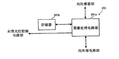
Among Fig. 3 and Fig. 4, liquid-crystal apparatus 1 constitutes and comprises: sensor control circuit portion 201, backlight lamp control circuit part 202, display control circuit portion 203, sensor part 204, display part 205 and backlight 206.
Here, with reference to Fig. 4, the detailed formation of sensor control circuit portion 201 is described.As shown in Figure 4, sensor control circuit portion 201 constitutes and comprises 201a of image processing circuit portion and storer 201b.The 201a of image processing circuit portion has the data of the image of indicating mechanism to handle to shooting when indicating mechanisms such as detection finger.Storer 201b stores the data of supplying with from the 201a of image processing circuit portion.The 201a of image processing circuit portion reads the data that storer 201b is stored in good time, uses when determining the position of indicating mechanism.In addition, the location determining method determined of the position of the indicating mechanism of finger on 201 couples of display surface 20s of sensor control circuit portion etc. describes in detail in the back.
Get back to Fig. 3 once more, backlight lamp control circuit part 202 controls the action of backlight 206 based on from external circuit portion 207 and sensor control circuit portion 201 difference signal supplied.Backlight 206 penetrates light source light to display surface 20s under the control of backlight lamp control circuit part 202, this light source light is used to detect the situation of having indicated the display surface 20s of liquid-crystal apparatus 1 with indicating mechanisms such as fingers.And backlight 206 also is also used as the demonstration light source that penetrates display light, and this display light is used for showing on display surface and the corresponding image of supplying with through backlight lamp control circuit part 202 from external circuit portion 207 of picture signal.According to such backlight 206, need not to be provided in addition to penetrate the light source of the light that detects the detection usefulness that indicating mechanism uses, therefore, the formation of liquid-crystal apparatus 1 is simplified.
<1-3: the formation of pixel portions 〉
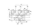
Then, with reference to Fig. 5~Fig. 9, the formation of the pixel portions of liquid-crystal apparatus 1 is elaborated.Fig. 5 is the equivalent electrical circuit that constitutes various elements in a plurality of pixels of rectangular formation of image display area 10a of liquid-crystal apparatus 1, wiring etc., and Fig. 6 is an equivalent circuit diagram of having represented the equivalent electrical circuit of sensor part 204 with pixel portions.Fig. 7 is the vertical view of adjacent a plurality of pixel groups that has formed the tft array substrate of data line, sweep trace, pixel electrode etc.Fig. 8 is the VIII-VIII ' cut-open view of Fig. 7.Fig. 9 is the IX-IX ' cut-open view of Fig. 7.In addition, in Fig. 8 and Fig. 9, in order to make each layer, each parts for discerning the size of degree on scheme, each layer, each parts have changed engineer's scale by this.
Among Fig. 5, each of a plurality of pixel portions 72 of the rectangular formation of the image display area 10a of formation liquid-crystal apparatus 1 constitutes and comprises: show the red 72R of sub-pixel portion, show green 72G of sub-pixel portion and the blue 72B of sub-pixel portion of demonstration.Therefore, liquid-crystal apparatus 1 is the display device of energy color display.Each of the 72R of sub-pixel portion, 72G and 72B possesses pixel electrode 9a, TFT30 and liquid crystal cell 50a.TFT30 is electrically connected with pixel electrode 9a, when liquid-crystal apparatus 1 action pixel electrode 9a is carried out switch control.The data line 6a that is supplied to picture signal is electrically connected with the source electrode of TFT30.Picture signal S1, the S2 that writes to data line 6a ..., Sn also can supply with by line in proper order successively with this, also can supply with by group many adjacent data line 6a.
Sweep trace 3a is electrically connected with the grid of TFT30, liquid-crystal apparatus 1 constitute predetermined timing with pulse mode with sweep signal G1, G2 ..., Gm imposes on sweep trace 3a with this order successively by line.Pixel electrode 9a is electrically connected with the drain electrode of TFT30, by making closed this switch during certain only as the TFT30 of on-off element, make predetermined timing write the picture signal S1, the S2 that supply with from data line 6a ..., Sn.By pixel electrode 9a be written to the specified level of liquid crystal picture signal S1, S2 ..., Sn be held between the opposite electrode that forms on the counter substrate certain during.
Liquid crystal that liquid crystal layer 50 is comprised is modulated light thus according to the voltage level that is applied in and the orientation or the order of elements collection can change, and can realize gray level display.If normal white pattern, being unit with each sub-pixel portion then reduces transmitance at incident light according to the voltage that is applied in, if normal black mode, being unit with each sub-pixel portion then increases transmitance at incident light according to the voltage that is applied in, and penetrates the light with contrast corresponding with picture signal from liquid-crystal apparatus 1 as a whole.In order to prevent that picture signal from leaking, and the liquid crystal cell 50a that forms between image electrode 9a and the opposite electrode is added with in parallel and accumulates electric capacity 70.
Among Fig. 6, image display area 10a on tft array substrate 10, be formed with sensor part 204 by each pixel portions 72, this sensor part 204 constitutes and comprises: TFT211a, 211b and 211c, as the photodiode 212 and the capacity cell 213 of the example of " photo detector " of the present invention.
The grid of TFT211a is electrically connected with sensor precharge control line 302.The source electrode of TFT211a and drain electrode are electrically connected with pre-charge line 301 and photodiode 212 and capacity cell 213 respectively.
TFT211a comes switched conductive to end according to the precharge control signal of supplying with through sensor precharge control line 302 from sensor control circuit portion 201.Photodiode 212 by the pre-charge voltage of supplying with through pre-charge line 301 and TFT211a by precharge.
The grid of TFT211b is electrically connected with photodiode 212, is the amplification element that the variation of the quantity of electric charge that photodiode 212 is accumulated is amplified.The variation of the quantity of electric charge that produces in the photodiode 212 causes because of the reflected light that photodiode 212 is detected.
The grid of TFT211c is electrically connected with sensor output control line 303.TFT211c comes switched conductive to end according to the output control signal of supplying with through sensor output control line 303, and the output signal corresponding with the variation of the quantity of electric charge that produces in the photodiode 212 outputed to sensor control circuit portion 201 through sensor output line 304.
Then, with reference to Fig. 7~Fig. 9, the concrete formation of the 72s of sub-pixel portion that constitutes pixel portions is described.
Among Fig. 7 and Fig. 8, on the tft array substrate 10 of liquid-crystal apparatus 1, with the rectangular a plurality of transparent pixel electrode 9a (by dotted line part 9a ' expression profile) that are provided with, be provided with data line 6a and sweep trace 3a with respect to directions X and Y direction along each border in length and breadth of pixel electrode 9a.Contact with the display surface 20s of liquid-crystal apparatus 1 or the desirable zone of indicated number face 20s by indicating mechanisms such as fingers, thus can be to the various information of liquid-crystal apparatus 1 input.
Sweep trace 3a is configured to: opposed with the channel region 1a ' that hatched example areas upper right among Fig. 4 of semiconductor layer 1a is represented.Be provided with the TFT30 that pixel switch is used everywhere what sweep trace 3a and data line 6a intersected.
Make with high concentration drain region 1e be connected with pixel electrode 9a as the bottom capacitance electrode 71 of pixel current potential lateral capacitance electrode and as the part of the top capacitor electrode 300 of set potential lateral capacitance electrode across dielectric film 75 arranged opposite, formed thus and accumulated electric capacity 70.
As shown in Figure 7 and Figure 8, top capacitor electrode 300 for example is arranged on the upside of TFT30 as comprising the upper light shielding (built-in photomask) of metal or alloy.Top capacitor electrode 300 is also as set potential lateral capacitance electrode performance function.Top capacitor electrode 300 is for example by at least one metal monomer, alloy, metal silicide, the poly-stacked formations such as structure that form of silicide that comprises in Ti (titanium), Cr (chromium), W (tungsten), Ta (tantalum), Mo (molybdenum), Pd (palladium), the Al metals such as (aluminium).Top capacitor electrode 300 for example also can have the multi-ply construction that second film-stack that first film that is made of the polysilicon film of electric conductivity etc. and the metal silicide film that comprises refractory metal etc. constitute forms.
The dielectric film 75 of configuration between as the bottom capacitance electrode 71 of capacitance electrode and top capacitor electrode 300 is for example by formations such as the silicon oxide film of HTO (High Temperature Oxide) film, LTO (LowTemperature Oxide) film etc. or silicon nitride films.
Be arranged on the downside photomask 11a of TFT30 downside across underlying insulation film 12 with lattice-shaped, the channel region 11a of TFT30 and periphery thereof blocked the back light of incident in tft array substrate 10 lateral device.Downside photomask 11a and top capacitor electrode 300 are same, are made of at least one metal monomer, alloy, metal silicide, the poly-stacked structure that forms of silicide etc. that comprise in the metals such as Ti, Cr, W, Ta, Mo, Pd, Al for example.
Underlying insulation film 12 is except that TFT30 and downside photomask 11a are carried out the function of layer insulation, chap when preventing from the surface of tft array substrate 10 ground, make the function of pixel switch with the deterioration in characteristics of TFT30 because of cleaning the residual dirt in back etc. by being formed on whole of tft array substrate 10, also having.Pixel electrode 9a is by carrying out relaying to bottom capacitance electrode 71, is electrically connected with high concentration drain region 1e among the semiconductor layer 1a through contact hole 83 and 85.
As shown in Figure 7 and Figure 8, liquid-crystal apparatus 1 comprise transparent tft array substrate 10 and with the transparent counter substrate 20 of these tft array substrate 10 arranged opposite.Tft array substrate 10 for example is made of quartz base plate, glass substrate, silicon substrate, and counter substrate 20 for example is made of glass substrate or quartz base plate.
Be provided with opposite electrode 21 in whole on counter substrate 20, its downside is provided with the alignment films 22 after the orientation process that has been implemented regulations such as friction treatment.Opposite electrode 21 for example is made of transparent and electrically conductive films such as ITO films.Alignment films 22 is made of organic membrane such as polyimide films.
The photomask of lattice-shaped or vertical bar shape also can be set on the counter substrate 20.By adopting such formation, with as top capacitor electrode 300 and the upper light shielding that is provided with can stop more reliably from the incident light of counter substrate 20 sides and invade to channel region 1a ' and periphery thereof.
Adopt such formation, between the tft array substrate 10 and counter substrate 20 that dispose according to the mode that makes pixel electrode 9a and opposite electrode 21 opposites, form liquid crystal layer 50.Liquid crystal layer 50 is in the state of orientation of regulation by alignment films 16 and 22 under being not applied to from the state of the electric field of pixel electrode 9a.
Among Fig. 8, pixel switch has LDD (Lightly Doped Drain) structure with TFT30, comprising: gate electrode 3a2, by the electric field from sweep trace 3a form the semiconductor layer 1a of raceway groove channel region 1a ', comprise dielectric film 2, low concentration source region 1b and low concentration drain region 1c, the high concentration source region 1d and the high concentration drain region 1e that make the gate insulating film that sweep trace 3a and semiconductor layer 1a insulate.Low concentration source region 1b, low concentration drain region 1c, high concentration source region and high concentration drain region 1e have constituted the extrinsic region of semiconductor layer 1a, form the minute surface symmetry in the both sides of channel region 1a '.
Gate electrode 3a2 is formed by the conducting film of polysilicon film etc. or at least one the metal monomer, alloy, metal silicide, the poly-stacked structure that forms of silicide etc. that comprise in the metals such as Ti, Cr, W, Ta, Mo, Pd, Al for example, according to being arranged on the channel region 1a ' across dielectric film 2 with low concentration source region 1b and the low concentration drain region nonoverlapping mode of 1c.Therefore, in TFT30, fully guaranteed the skew of high concentration source region 1d and high concentration drain region 1e and gate electrode 3a2.
In addition, the edge of gate electrode 3a2 is overlapping on the border of overlooking observation down and low concentration source region 1b, low concentration drain region 1c and channel region 1a ', and the stray capacitance that produces between low concentration source region 1b and low concentration drain region 1c and the gate electrode 3a2 is lowered.Thus, can realize the transistorized high speed motion of TFT30, improve the display performance of liquid-crystal apparatus 1.
And, in liquid-crystal apparatus 1, by being formed on the top capacitor electrode 300 on the gate electrode 3a2 according to the mode that covers TFT30, compare with the situation of only carrying out shading by gate electrode 3a2, can be effectively to low concentration source region 1b and the 1c shading of low concentration drain region.
Like this, according to liquid-crystal apparatus 1, the TFT30 that utilizes the light leakage current to be lowered can reduce flicker and waiting the unfavorable condition that produces when image shows carrying out, can be with high-quality display image.And because TFT30 has LDD structure, therefore, the cut-off current that flows among low concentration source region 1b and the low concentration drain region 1c when the non-action of TFT30 is lowered, and the reduction of the conducting electric current that flows when having suppressed the TFT30 action.Therefore, according to liquid-crystal apparatus 1, can utilize the advantage and the almost immobilising fact of light leakage current of LDD structure, with high-quality display image.
On dielectric film 2, sweep trace 3a and gate electrode 3a2, be formed with first interlayer dielectric 41, offer contact hole 81 that leads to high concentration source region 1d and the contact hole 83 that leads to high concentration drain region 1e on it respectively.
On first interlayer dielectric 41, be formed with bottom capacitance electrode 71 and top capacitor electrode 300, be formed with second interlayer dielectric 42 of having offered contact hole 81 and 85 respectively on these electrodes.
And then whole the mode that goes up according to covering second interlayer dielectric 42 from data line 6a has for example formed the 3rd interlayer dielectric 43 that offers contact hole 85 by bpsg film.Pixel electrode 9a and alignment films 16 be arranged on the 3rd interlayer dielectric 43 above.In addition, the 3rd interlayer dielectric 42 also can utilize the photonasty acryl resin to wait to reduce jump.
Then, with reference to Fig. 7 and Fig. 9, photodiode 212 is elaborated.
As Fig. 7 and shown in Figure 9, photodiode 212 is formed on non-open area, and this non-open area makes the open area that helps image to show in fact isolate mutually in image display area 10a.The open area is to make the zone of using light transmission from the demonstration of backlight 206 ejaculations.The non-open area that such open area is formed non-permeability films such as data line 6a surrounds.In the open area, the demonstration of penetrating from backlight 206 is used up according to the state of orientation of liquid crystal layer 50 and modulated, penetrates from display surface 20s as light modulated.
<1-4: based on the location determining method of the indicating mechanism of display device 〉
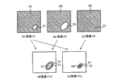
Then, with reference to Figure 10~Figure 15, the location determining method based on the indicating mechanism of liquid-crystal apparatus 1 is described.Figure 10 is the process flow diagram of the location determining method of the indicating mechanism that can be carried out by the liquid-crystal apparatus 1 of present embodiment.Figure 11 is the skeleton diagram of liquid-crystal apparatus 1 of having represented the light path of light source light, reflected light and outer light with diagram.Figure 12 is by the concept map of the various images of Flame Image Process from conceptive expression sensor control circuit portion.In addition, in Figure 12, enumerated example by the big situation of the light intensity of light outside the catoptrical light strength ratio of indicating mechanisms such as finger reflection.Figure 13 is a concept map of having represented to have each light source beam light of different mutually light intensities along time shaft with diagram.Figure 14 is the variation of concept map shown in Figure 12.Figure 15 is the concept map of the notion of the principle that will remove by the noise that image was comprised that photodiode 212 is obtained with diagram expression
Among Figure 10, Figure 11 and Figure 12, when indicating mechanisms such as finger were detected, backlight 206 penetrated the light source light La1 with light intensity A1 from the rear side of display surface 20s towards display surface 20s.Light source light La1 is that the surface of finger F is reflected in an example of the indicating mechanism that the optional position of display surface 20s is indicated, the reflected light Lb1 that is detected as an example of " a branch of reflected light " of the present invention by photodiode 212.Parallel therewith, display surface 20s not with the finger F overlapping areas, detect outer light Ld by photodiode 212.Sensor control circuit portion 201 obtains from the output signal of each photodiode 212 output, generate the image section F1 that comprises the finger F corresponding with light source light La1 with light intensity A1 and with the image P1 of the corresponding image section Q1 of outer light Ld.Image P1 is an example of " first image " of the present invention.Storer 201b obtains the brightness data of image P1 and stores (step S10) from image processing circuit portion 201.
Then, backlight 206 penetrates the multi beam light source light with light intensity different with light source light La1 to display surface 20s successively.Therefore, light source light La1 penetrates to display surface 20s from backlight 206 with mutual different timing with the multi beam light source light with light intensity different with light source light La1.
Here, with reference to Figure 13, the light source light that penetrates with mutually different timings from backlight 206 and have different mutually light intensities is described.
Among Figure 13, each the bundle T1 between the first phase with multi beam light source light La1 of light intensity A1 penetrates with pulse type.After T1 between the first phase, at the second phase T2 that arrives successively with between the third phase among the T3, backlight 206 penetrates multi beam light source light La2 with light intensity A2 and the multi beam light source light La3 with light intensity A3 to display surface 20s.Light intensity A2 maximum in light intensity A1, A2 and A3, light intensity A3 minimum.Because backlight 206 constitutes and comprises light emitting diode, therefore,, can correctly set the light intensity of each light source light by under the control of backlight lamp control circuit part 202, setting input current individually to the light emitting diode input.And, according to backlight 206 with light emitting diode, can also correctly control the fluorescent lifetime of each light emitting diode, therefore, comprise each bundle based on light source light La1, La2 and La3 by the reflected light after the finger F reflection and the brightness data of the image of the image section of definite finger F is determined by unique according to each catoptrical light intensity.
As shown in figure 11, reflected light Lb2 after each bundle of light source light La2 and La3 is reflected by finger F and each bundle of Lb3 are examples of " other reflected light of multi beam " of the present invention, because of the light intensity of each bundle of light source light La2 and La3 is different mutually, the light intensity of each bundle of reflected light Lb1, Lb2 and Lb3 is different mutually.Therefore, the image of definite finger F is also different mutually by each bundle that detects these reflected light Lb1, Lb2 and Lb3.
Return Figure 10, Figure 11 and Figure 12 once more, after storer 201b stores the brightness data of image P1, penetrate light source light La2 and La3 successively from backlight 206, and by photodiode 212 detection of reflected light Lb2 and Lb3.Image processing circuit 201a generates the image section of the finger F corresponding with each bundle of reflected light Lb2 and Lb3 successively.Each of image P2 and P3 is each the example of " second image " of the present invention, by the brightness data (step S20 and S30) of storer 201b memory image P2 successively and P3.
In addition, because light source light La1, La2 and La3 be interior ejaculation of utmost point short time of the unchanged degree of light intensity of light Ld outside, therefore, can think that each image P1, P2 and P3 comprised except that image section F1, the F2 of finger and the brightness of other image sections Q1, Q2 the F3 and Q3 also be certain.
Also have, as shown in figure 12, image section F1, the F2 of the finger F that each comprised of image P1, P2 and P3 and the size of F3, because of the light intensity of each bundle of reflected light Lb1, Lb2 and Lb3 different mutually.
Then, as Figure 10 and shown in Figure 12, image processing circuit 201a reads image P1, P2 and P3 brightness data separately from storer 201b, generates image P12 and P13 (step S40).Each of image P12 and P13 is an example of " the 3rd image " of the present invention, and image P12 generates by the difference value of computed image P1 and image P2 brightness data separately.Image P13 and image P12 are same, and the difference value by computed image P1 and image P3 brightness data separately generates.
As shown in figure 12, the 201a of image processing circuit portion determines that at image P12 public part is the centre coordinate C1 of image section F1 among the image section F1 of the finger F that obtains according to each reflected light and the F2.Equally, the 201a of image processing circuit portion determines that at image P13 public part is the centre coordinate C2 (step S50) of image section F3 among the image section F1 of the finger F that obtains according to each reflected light and the F2.Here, image section Q1, Q2 and Q3 in each of image P1, P2 and P3 have public brightness data, and therefore, the difference of the brightness data by obtaining these images is cancelled.
Then, the 201a of image processing circuit portion determines the position (step S60) of finger F in the face of display surface 20s by the mean value of coordinate C1 of computing center and C2.
Through above step, liquid-crystal apparatus 1 can correctly be determined the position of indicating mechanisms such as finger, and can import the various information corresponding with the position of finger F.And, the light source light that penetrates for the position of determining indicating mechanisms such as finger penetrates with pulse type with respect to time shaft, even therefore have different light intensity mutually, also can be by according to making time average mode about equally adjust pulse width, thereby can not change, therefore can under the display quality situation that power consumption of deterioration and backlight does not increase, correctly determine the position of indicating mechanisms such as finger from visually recognizing brightness.Further specifically, as shown in figure 13, the pulse width maximum of the light source light La3 of light intensity minimum among light source light La1, La2 that penetrates with pulse type and the La3, the pulse width minimum of the light source light La2 of light intensity maximum.Therefore, during the light source light La1, the La2 that penetrate in each of T1, T2 and T3 and La3 integrated value mutually about equally, the brightness when the eye-observation image takes place hardly changes.
And, also short by the pulse width of the shortest light source light of pulse width in the time ratio light source light that makes the light detection, thus can not exert an influence to the light accuracy of detection yet.
Then, with reference to Figure 14, illustrate that the light intensity by the outer light of catoptrical light strength ratio of indicating mechanism reflection is little, with the flow process of above-mentioned location determining method in the magnitude relationship of the mutual light intensity of the reflected light that uses and outer light compare each image that generates under the big or small opposite situation of reflected light with respect to the light intensity of outer light.
Among Figure 14, by generating image P1 ', P2 ' and P3 ' by photodiode 212 detection of reflected light Lb1, Lb2 and Lb3.Here, because the light intensity of the outer light Ld of reflected light Lb1, Lb2 and Lb3 light strength ratio separately is little, therefore, the image section around brightness ratio image section F1 ', the F2 ' of image section F1 ', the F2 ' of finger F and F3 ' and the F3 ' is little.But owing to can think that also the brightness of outer light Ld is certain, therefore, in the image P12 ' that the difference value based on image P1 ', P2 ' brightness data separately generates, the brightness around image section F1 ', the F2 ' offsets.Equally, in the image P13 ' that each the difference value of brightness data based on image P1 ', P3 ' generates, the brightness around image section F1 ', the F3 ' also offsets.Therefore, the centre coordinate C2 ' of the image section F3 ' that centre coordinate C1 ' by the overlapped image section F1 ' of computed image part F1 ' and F2 ' and image section F1 ' and F3 ' are overlapped can correctly determine the position of finger F.
In addition, in the present embodiment, illustrated by computed image P12, P13, the mean value of the centre coordinate of the image section that the profile to indicating mechanism that each of P12 ' and P13 ' comprised is stipulated, determine the example of the position of indicating mechanisms such as finger, but according to the location determining method that can carry out by display device of the present invention, owing to also thinking image P12, P13, the image section of the indicating mechanism that each of P12 ' and P13 ' comprised shared scope in these images, with the actual scope that occupies in the zone of indicating mechanism on display surface 20s about equally, therefore, even do not calculate the position that the mean value of centre coordinate also can be determined indicating mechanism with precision to a certain degree.
And, liquid-crystal apparatus 1 according to present embodiment, since need not to add optical sensor such as photodiode voltage level the adjustment circuit or adjust the light timing adjusting circuit of detection time, therefore, it is complicated that the circuit of control circuit of the action usefulness of control optical sensor is constituted, and the circuit of liquid-crystal apparatus 1 constituted simplify.
Then, with reference to Figure 15, other advantages that location determining method had of present embodiment are described.As shown in figure 15, in each of image P1 ' and P2 ', comprise the image section of the foreign matter K different, promptly comprise under the situation of noise, the definite precision when this noise can be reduced in the position of determining indicating mechanism with finger F.But according to the location determining method that can be carried out by the liquid-crystal apparatus 1 of present embodiment, the image section of foreign matter K can be offset by the difference value of computed image P1 ' and P2 ' brightness data separately, can not remain among the image P12 '.Therefore, according to the location determining method that can carry out by the liquid-crystal apparatus 1 of present embodiment, the noise contribution of the definite precision reduction in the time of getting rid of the position that may make definite indicating mechanism, thus can determine the position of indicating mechanism with high precision.
As mentioned above, according to the liquid-crystal apparatus 1 of present embodiment and the location determining method that can carry out by the liquid-crystal apparatus 1 of present embodiment, can irrespectively constitute the position of to determine accurately the indicating mechanism on the display surface with the magnitude relationship of outer light and light source light relative light intensity separately by simple circuit.Therefore, according to the liquid-crystal apparatus 1 of present embodiment, can be according to the position of determined indicating mechanism, correctly to this liquid-crystal apparatus 1 input information.
<2: electronic equipment 〉
Then, with reference to Figure 16 and Figure 17, the embodiment of the electronic equipment that constitutes possessing above-mentioned liquid-crystal apparatus describes.
Figure 16 is a stereographic map of having used the portable personal computer of above-mentioned liquid-crystal apparatus.Among Figure 16, computing machine 1200 constitutes to be possessed: comprise the main part 1204 of keyboard 1202 and comprise above-mentioned liquid-crystal apparatus and the liquid crystal display 1206 that constitutes.Liquid crystal display 1206 constitutes by add backlight at the back side of liquid crystal panel 1005, has touch panel function, and has improved display quality because of high numerical aperture.
Then, the example of having used above-mentioned liquid-crystal apparatus in mobile phone is described.Figure 17 is the stereographic map as the mobile phone of an example of the electronic equipment of present embodiment.Among Figure 17, mobile phone 1300 possesses: a plurality of action buttons 1302, the liquid-crystal apparatus 1005 that adopts reflection-type display format and have same formation with above-mentioned liquid-crystal apparatus.According to mobile phone 1300, improved numerical aperture, can realize that high quality images shows, and, can pass through display surface input information correctly by indicating mechanisms such as fingers.
Claims (6)
1, a kind of display device comprises:
Light source, its from by the rear side of the display surface of indicating mechanism indication towards described display surface, have the multi beam light source light of different mutually light intensities with different pulsed exposure mutually;
Testing agency, it is arranged on described rear side, and the multi beam reflected light that is reflected by described indicating mechanism in the described multi beam light source light is detected; With
Determine mechanism, its calculate based on a branch of reflected light that described multi beam reflected light comprised and the brightness data of the first definite image with based on other catoptrical each bundles of multi beam that have the light intensity different in the described multi beam reflected light and the difference value of the brightness data of definite a plurality of second images with described a branch of catoptrical light intensity, and, determine the position of described indicating mechanism based on each of each a plurality of the 3rd images of determining of a plurality of difference values of calculating according to this.
2, display device according to claim 1 is characterized in that,
The mean value of the centre coordinate of the image section of the described indicating mechanism that each comprised of described definite mechanism by calculating described a plurality of the 3rd images is determined described position.
3, display device according to claim 1 and 2 is characterized in that, also comprises:
Substrate, it is configured between described light source and the described display surface; With
A plurality of pixel portions constitute the viewing area on the described substrate,
Described testing agency comprises the photo detector that is formed on non-open area, and described non-open area makes the open area of described pixel portions isolate mutually in described viewing area.
4, according to each described display device in the claim 1~3, it is characterized in that,
Described light source is also used as the demonstration light source, and the display light that is used for showing the image corresponding with picture signal on described display surface is penetrated in this demonstration with light source.
5, according to each described display device in the claim 1~4, it is characterized in that,
Described light source constitutes and comprises light emitting diode.
6, a kind of electronic equipment constitutes and possesses each described display device in the claim 1~5.
Applications Claiming Priority (2)
| Application Number | Priority Date | Filing Date | Title |
|---|---|---|---|
| JP2007061506A JP4826512B2 (en) | 2007-03-12 | 2007-03-12 | Display device and electronic device |
| JP2007-061506 | 2007-03-12 |
Publications (1)
| Publication Number | Publication Date |
|---|---|
| CN101266529A true CN101266529A (en) | 2008-09-17 |
Family
ID=39843649
Family Applications (1)
| Application Number | Title | Priority Date | Filing Date |
|---|---|---|---|
| CNA2008100852203A Pending CN101266529A (en) | 2007-03-12 | 2008-03-10 | Display device and electronic device |
Country Status (3)
| Country | Link |
|---|---|
| US (1) | US20080259051A1 (en) |
| JP (1) | JP4826512B2 (en) |
| CN (1) | CN101266529A (en) |
Cited By (15)
| Publication number | Priority date | Publication date | Assignee | Title |
|---|---|---|---|---|
| CN101853109A (en) * | 2009-03-31 | 2010-10-06 | 硅谷实验室公司 | Be used for optical proximity sensing and touch equipment and the method that input is controlled |
| CN102063227A (en) * | 2009-11-18 | 2011-05-18 | 罗伯特.博世有限公司 | Display device capable of being manually controlled |
| CN102096531A (en) * | 2011-02-18 | 2011-06-15 | 福州华映视讯有限公司 | Operation method for optical touch display device |
| CN102473073A (en) * | 2009-08-27 | 2012-05-23 | 索尼公司 | Information processing device, information processing method, and program |
| CN102467300A (en) * | 2010-11-05 | 2012-05-23 | 精工爱普生株式会社 | Optical detection device, electronic apparatus, and optical detection method |
| CN102541363A (en) * | 2010-12-16 | 2012-07-04 | 精工爱普生株式会社 | Optical position detection device and apparatus with position detection function |
| CN102750016A (en) * | 2011-04-04 | 2012-10-24 | 精工爱普生株式会社 | Input system and pen-shaped input device |
| CN103125115A (en) * | 2010-10-04 | 2013-05-29 | 索尼公司 | Information processing apparatus, information processing system and information processing method |
| CN103186291A (en) * | 2011-12-29 | 2013-07-03 | 原相科技股份有限公司 | Optical touch system |
| CN103309516A (en) * | 2012-03-13 | 2013-09-18 | 原相科技股份有限公司 | Optical touch device and detection method thereof |
| CN105027052A (en) * | 2012-09-21 | 2015-11-04 | 亚马逊技术有限公司 | Display integrated camera array |
| WO2018049840A1 (en) * | 2016-09-19 | 2018-03-22 | 京东方科技集团股份有限公司 | Display device and method for controlling brightness of display device |
| CN108153053A (en) * | 2018-01-02 | 2018-06-12 | 京东方科技集团股份有限公司 | A kind of display device and driving method |
| WO2019041631A1 (en) * | 2017-08-29 | 2019-03-07 | 惠科股份有限公司 | Display panel |
| CN110226194A (en) * | 2018-05-31 | 2019-09-10 | 京东方科技集团股份有限公司 | Display panel, display equipment, display base plate, manufacture display panel and the method for showing equipment |
Families Citing this family (37)
| Publication number | Priority date | Publication date | Assignee | Title |
|---|---|---|---|---|
| WO2009081810A1 (en) * | 2007-12-20 | 2009-07-02 | Sharp Kabushiki Kaisha | Display device having optical sensor |
| US20100271335A1 (en) * | 2008-01-25 | 2010-10-28 | Toshimitsu Gotoh | Display device having optical sensors |
| WO2009104667A1 (en) * | 2008-02-21 | 2009-08-27 | シャープ株式会社 | Display device provided with optical sensor |
| WO2009110293A1 (en) * | 2008-03-03 | 2009-09-11 | シャープ株式会社 | Display device with light sensors |
| JP5148685B2 (en) * | 2008-03-21 | 2013-02-20 | シャープ株式会社 | LCD device with built-in touch sensor |
| TWI409537B (en) * | 2008-04-03 | 2013-09-21 | Innolux Corp | Liquid crystal panel and liquid crystal display device using same |
| JP2009250772A (en) * | 2008-04-04 | 2009-10-29 | Sony Corp | Position detection system, position detection method, program, object determination system and object determination method |
| WO2010038530A1 (en) * | 2008-09-30 | 2010-04-08 | シャープ株式会社 | Display panel and display panel inspection method |
| TWI403940B (en) * | 2008-12-03 | 2013-08-01 | Au Optronics Corp | Detecting method for photo sensor touch panel and touch control electronic apparatus using the same |
| US8363894B2 (en) * | 2008-12-12 | 2013-01-29 | Silicon Laboratories Inc. | Apparatus and method for implementing a touchless slider |
| CN101762922B (en) | 2008-12-24 | 2012-05-30 | 京东方科技集团股份有限公司 | Touch type electronic paper and manufacture method thereof |
| JP5481902B2 (en) * | 2009-03-27 | 2014-04-23 | ソニー株式会社 | Display panel and display device |
| JP5178631B2 (en) | 2009-05-26 | 2013-04-10 | 株式会社ジャパンディスプレイウェスト | Touch sensor, display device, and electronic device |
| WO2010137219A1 (en) * | 2009-05-28 | 2010-12-02 | シャープ株式会社 | Touch panel, liquid crystal panel, liquid crystal display device, and liquid crystal display device incorporating touch panel |
| KR20110009973A (en) * | 2009-07-23 | 2011-01-31 | 삼성전자주식회사 | Display system and method of cotrolling the display system |
| TWI421751B (en) * | 2009-08-25 | 2014-01-01 | Au Optronics Corp | Touch device, display substrate, liquid crystal display and operation method for photo sensor |
| JP5740132B2 (en) * | 2009-10-26 | 2015-06-24 | 株式会社半導体エネルギー研究所 | Display device and semiconductor device |
| JP5326989B2 (en) * | 2009-10-26 | 2013-10-30 | セイコーエプソン株式会社 | Optical position detection device and display device with position detection function |
| JP5493702B2 (en) * | 2009-10-26 | 2014-05-14 | セイコーエプソン株式会社 | Projection display with position detection function |
| JP2011099994A (en) | 2009-11-06 | 2011-05-19 | Seiko Epson Corp | Projection display device with position detecting function |
| KR101754382B1 (en) | 2010-03-11 | 2017-07-05 | 가부시키가이샤 한도오따이 에네루기 켄큐쇼 | Semiconductor device |
| JP5792524B2 (en) * | 2010-07-02 | 2015-10-14 | 株式会社半導体エネルギー研究所 | apparatus |
| JP5745369B2 (en) | 2010-09-06 | 2015-07-08 | 株式会社半導体エネルギー研究所 | Electronics |
| CN102622131B (en) * | 2011-01-28 | 2015-04-29 | 联想(北京)有限公司 | Electronic equipment and positioning method |
| US8836672B2 (en) * | 2011-02-09 | 2014-09-16 | Dornerworks, Ltd. | System and method for improving machine vision in the presence of ambient light |
| TWI439907B (en) * | 2012-02-29 | 2014-06-01 | Pixart Imaging Inc | Optical touch device and detection method thereof |
| US9465429B2 (en) | 2013-06-03 | 2016-10-11 | Qualcomm Incorporated | In-cell multifunctional pixel and display |
| US20140368470A1 (en) * | 2013-06-13 | 2014-12-18 | Samsung Display Co., Ltd. | Adaptive light source driving optical system for integrated touch and hover |
| CN105677116B (en) * | 2016-04-06 | 2018-07-10 | 京东方科技集团股份有限公司 | A kind of touch-control structure, touch screen and display device |
| KR102365543B1 (en) * | 2016-06-10 | 2022-02-18 | 가부시키가이샤 한도오따이 에네루기 켄큐쇼 | Information terminal |
| JP2018045034A (en) * | 2016-09-13 | 2018-03-22 | 株式会社ジャパンディスプレイ | Display device |
| CN107092124A (en) * | 2017-05-11 | 2017-08-25 | 京东方科技集团股份有限公司 | A kind of array base palte and preparation method thereof, display device |
| KR102439147B1 (en) * | 2017-12-29 | 2022-08-31 | 엘지디스플레이 주식회사 | Display device |
| US10572070B2 (en) * | 2018-06-25 | 2020-02-25 | Vanguard International Semiconductor Corporation | Optical devices and fabrication method thereof |
| US10817018B1 (en) | 2019-04-29 | 2020-10-27 | Apple Inc. | Electronic devices with ambient light sensors and emissive displays |
| CN110750020B (en) * | 2019-10-31 | 2022-10-18 | 厦门天马微电子有限公司 | Display module and display device |
| CN111029343A (en) * | 2019-11-13 | 2020-04-17 | Tcl华星光电技术有限公司 | Array substrate and preparation method thereof |
Family Cites Families (10)
| Publication number | Priority date | Publication date | Assignee | Title |
|---|---|---|---|---|
| EP0837418A3 (en) * | 1996-10-18 | 2006-03-29 | Kabushiki Kaisha Toshiba | Method and apparatus for generating information input using reflected light image of target object |
| JP3267218B2 (en) * | 1997-11-27 | 2002-03-18 | 松下電器産業株式会社 | Liquid crystal display with image reading function |
| US7859519B2 (en) * | 2000-05-01 | 2010-12-28 | Tulbert David J | Human-machine interface |
| JP4257221B2 (en) * | 2003-03-31 | 2009-04-22 | 東芝松下ディスプレイテクノロジー株式会社 | Display device and information terminal device |
| US7359564B2 (en) * | 2004-10-29 | 2008-04-15 | Microsoft Corporation | Method and system for cancellation of ambient light using light frequency |
| US7800594B2 (en) * | 2005-02-03 | 2010-09-21 | Toshiba Matsushita Display Technology Co., Ltd. | Display device including function to input information from screen by light |
| JP4630744B2 (en) * | 2005-02-03 | 2011-02-09 | 東芝モバイルディスプレイ株式会社 | Display device |
| JP4550619B2 (en) * | 2005-02-24 | 2010-09-22 | 東芝モバイルディスプレイ株式会社 | Flat display device and image capturing method thereof. |
| JP2006276223A (en) * | 2005-03-28 | 2006-10-12 | Sony Corp | Display apparatus and method |
| JP4618026B2 (en) * | 2005-07-12 | 2011-01-26 | ソニー株式会社 | Display device and detection method using display device for displaying and receiving light |
-
2007
- 2007-03-12 JP JP2007061506A patent/JP4826512B2/en not_active Expired - Fee Related
-
2008
- 2008-01-30 US US12/022,737 patent/US20080259051A1/en not_active Abandoned
- 2008-03-10 CN CNA2008100852203A patent/CN101266529A/en active Pending
Cited By (22)
| Publication number | Priority date | Publication date | Assignee | Title |
|---|---|---|---|---|
| CN101853109A (en) * | 2009-03-31 | 2010-10-06 | 硅谷实验室公司 | Be used for optical proximity sensing and touch equipment and the method that input is controlled |
| CN102473073B (en) * | 2009-08-27 | 2014-10-15 | 索尼公司 | Information processing device, information processing method, and program |
| CN102473073A (en) * | 2009-08-27 | 2012-05-23 | 索尼公司 | Information processing device, information processing method, and program |
| CN102063227A (en) * | 2009-11-18 | 2011-05-18 | 罗伯特.博世有限公司 | Display device capable of being manually controlled |
| CN102063227B (en) * | 2009-11-18 | 2016-02-24 | 罗伯特.博世有限公司 | Can the display device of Non-follow control |
| US9860484B2 (en) | 2010-10-04 | 2018-01-02 | Saturn Licensing Llc | Information processing apparatus, information processing system and information processing method |
| CN103125115A (en) * | 2010-10-04 | 2013-05-29 | 索尼公司 | Information processing apparatus, information processing system and information processing method |
| CN102467300A (en) * | 2010-11-05 | 2012-05-23 | 精工爱普生株式会社 | Optical detection device, electronic apparatus, and optical detection method |
| CN102467300B (en) * | 2010-11-05 | 2016-03-09 | 精工爱普生株式会社 | Optical detecting device, electronic equipment and optical profile type detection method |
| CN102541363A (en) * | 2010-12-16 | 2012-07-04 | 精工爱普生株式会社 | Optical position detection device and apparatus with position detection function |
| CN102096531A (en) * | 2011-02-18 | 2011-06-15 | 福州华映视讯有限公司 | Operation method for optical touch display device |
| CN102750016A (en) * | 2011-04-04 | 2012-10-24 | 精工爱普生株式会社 | Input system and pen-shaped input device |
| CN102750016B (en) * | 2011-04-04 | 2016-12-14 | 精工爱普生株式会社 | Input system and pen-based input equipment |
| CN103186291B (en) * | 2011-12-29 | 2015-12-02 | 原相科技股份有限公司 | Optical touch control system |
| CN103186291A (en) * | 2011-12-29 | 2013-07-03 | 原相科技股份有限公司 | Optical touch system |
| CN103309516A (en) * | 2012-03-13 | 2013-09-18 | 原相科技股份有限公司 | Optical touch device and detection method thereof |
| CN105027052A (en) * | 2012-09-21 | 2015-11-04 | 亚马逊技术有限公司 | Display integrated camera array |
| WO2018049840A1 (en) * | 2016-09-19 | 2018-03-22 | 京东方科技集团股份有限公司 | Display device and method for controlling brightness of display device |
| WO2019041631A1 (en) * | 2017-08-29 | 2019-03-07 | 惠科股份有限公司 | Display panel |
| US11287684B2 (en) | 2017-08-29 | 2022-03-29 | HKC Corporation Limited | Display device with automatic brightness adjustment |
| CN108153053A (en) * | 2018-01-02 | 2018-06-12 | 京东方科技集团股份有限公司 | A kind of display device and driving method |
| CN110226194A (en) * | 2018-05-31 | 2019-09-10 | 京东方科技集团股份有限公司 | Display panel, display equipment, display base plate, manufacture display panel and the method for showing equipment |
Also Published As
| Publication number | Publication date |
|---|---|
| JP2008224935A (en) | 2008-09-25 |
| US20080259051A1 (en) | 2008-10-23 |
| JP4826512B2 (en) | 2011-11-30 |
Similar Documents
| Publication | Publication Date | Title |
|---|---|---|
| CN101266529A (en) | Display device and electronic device | |
| US8212793B2 (en) | Liquid crystal device, image sensor, and electronic apparatus | |
| US8487911B2 (en) | Image display apparatus with image entry function | |
| CN101315476B (en) | Liquid crystal device and electronic apparatus | |
| KR101587284B1 (en) | Electro-optical device and electronic apparatus | |
| CN101447145B (en) | Display device and electronic apparatus | |
| US7755711B2 (en) | Liquid crystal device and electronic apparatus | |
| US8081147B2 (en) | Liquid crystal display device | |
| US8089476B2 (en) | Liquid crystal device | |
| US20070268206A1 (en) | Image display device | |
| JP3704889B2 (en) | Display device | |
| JP5125222B2 (en) | Liquid crystal device and electronic device | |
| US20120242636A1 (en) | Display device | |
| TW200941087A (en) | Display device | |
| JP5239317B2 (en) | Liquid crystal device and electronic device | |
| JP2009048145A (en) | Liquid crystal device, image sensor, and electronic device | |
| KR101258901B1 (en) | Liquid crystal display device having image sensing function | |
| KR101146375B1 (en) | Liquid Crystal Display Device Having Image Sensing Function | |
| JP5104023B2 (en) | Electro-optical device and electronic apparatus | |
| JP5256705B2 (en) | Electro-optical device and electronic apparatus | |
| JP2008083109A (en) | Display device | |
| JP2009109800A (en) | Liquid crystal device, image sensor, and electronic apparatus | |
| JP2010027829A (en) | Optical sensor, and liquid crystal display device using the optical sensor |
Legal Events
| Date | Code | Title | Description |
|---|---|---|---|
| C06 | Publication | ||
| PB01 | Publication | ||
| C10 | Entry into substantive examination | ||
| SE01 | Entry into force of request for substantive examination | ||
| AD01 | Patent right deemed abandoned |
Effective date of abandoning: 20080917 |
|
| C20 | Patent right or utility model deemed to be abandoned or is abandoned |